HAL Id: hal-00983587
https://hal.archives-ouvertes.fr/hal-00983587
Submitted on 25 Apr 2014
HAL is a multi-disciplinary open access
archive for the deposit and dissemination of
sci-entific research documents, whether they are
pub-lished or not. The documents may come from
teaching and research institutions in France or
abroad, or from public or private research centers.
L’archive ouverte pluridisciplinaire HAL, est
destinée au dépôt et à la diffusion de documents
scientifiques de niveau recherche, publiés ou non,
émanant des établissements d’enseignement et de
recherche français ou étrangers, des laboratoires
publics ou privés.
High-Impedance Surface Design Considerations
Julien Sarrazin, Anne-Claire Lepage, Xavier Begaud
To cite this version:
Julien Sarrazin, Anne-Claire Lepage, Xavier Begaud. High-Impedance Surface Design Considerations.
IEEE Antennas and Propagation Symposium, Jun 2012, Chicago, United States. pp.3569 - 3572,
�10.1109/APS.2004.1330117�. �hal-00983587�
High-Impedance Surface Design Considerations
Julien Sarrazin, Anne-Claire Lepage and Xavier Begaud
Institut Telecom, Telecom ParisTech LTCI Research Institute (UMR CNRS 5141)
Paris, France
Abstract—In this communication, High Impedance Surfaces
(HIS) based on patches are considered. The possibility to use the patch width as an additional degree of freedom for antennas is investigated. Within the limitation of a single linear polarization, rectangular patches allow adjusting the surface impedance value while keeping identical the in-phase reflection property of such metasurfaces on the same frequency range. With this approach, a bandwidth of 17% is achieved by using a dipole antenna over a HIS.
I. INTRODUCTION
Since their introduction in [1], High-Impedance Surfaces (HIS) have been extensively investigated in the field of antennas [2]. Such metasurfaces exhibit an in-phase reflection of incident waves, that makes them to behave like an Artificial Magnetic Conductor (AMC) within a limited frequency range. Consequently, HIS can be used as efficient reflectors while being located very close to the antenna. HIS usually associate a periodic array of printed elements with a grounded dielectric slab. The most common structure for the printed elements is the square patch with or without vias. This structure is easy to simulate and to fabricate and furthermore, some analytical models exist to predict their surface impedance [3].
However, patches do not have to be necessarily square [4]. HIS exhibit their exotic properties when patches resonate. Patches exhibit two orthogonal resonances. When the antenna located over the HIS is linearly polarized (such as a dipole for instance), only one resonance is sufficient to achieve the in-phase reflection. Thus, if the patch length is set in order to obtain a resonance at the desired frequency, the width may be set to any values. So while adjusting the patch width, it is therefore possible to control the surface impedance value without changing the resonance frequency responsible of the in-phase reflection.
Section II shows briefly the design of a classical patch based HIS. In section III, the effect of the patch width on the surface impedance is investigated and section IV presents how this additional degree of freedom is used in order to control the matching bandwidth of a dipole antenna over the HIS.
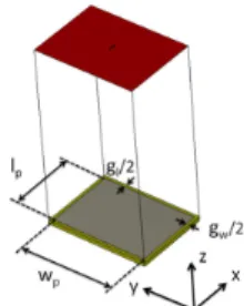
II. CLASSICAL DESIGN OF APATCH BASED HIS A HIS is classically characterized by the phase reflection method [1]. A single patch (without any vias), which constitutes the unit-cell in this communication, is simulated as
shown in Figure 1. PEC (Perfect Electric Conductor) conditions are applied on the sides lying in the YZ plane and PMC (Perfect Magnetic Conductor) conditions on the sides lying in the XZ plane. Consequently, a TEM wave is generated with the electric field polarized along the x-axis. With a patch length lp = 26.9 mm, a gap gl = 2.4 mm and an epoxy substrate
(εr = 4.3) of thickness h = 1.58 mm, the reflected phase is null
at 2.45 GHz in the patch plane. The HIS bandwidth is defined with the phase ranging between +/-90° and is equal to 0.15 GHz (Δf = 6%). The patch width wp and the gw do not
influence the reflected phase of this polarization. However, they do have an influence on the surface impedance and this effect is investigated in the next section.
Figure 1. Phase reflection simulation of the patch unit-cell.
III. INFLUENCE OF THE PATCH WIDTH ON THE SURFACE
IMPEDANCE
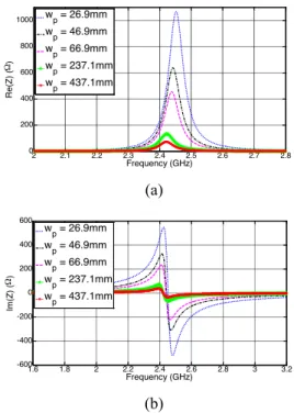
The influence of the patch width wp is investigated by
conducting a parametric study with values ranging from
wp = 26.9 mm (square patch) up to wp = 437.1 mm. Simulated
results of the surface impedance real part is shown in Figure 2a and of the imaginary part in Figure 2b. The response is a typical parallel resonant circuit response. It can be observed that for all values of wp, the impedance real part exhibits a
maximum and the imaginary part is null at f0 = 2.45 GHz. So
for any wp values, the resonance occurs at the same frequency
and so does the in-phase reflection.
However, the patch width largely influences the impedance value. For a square patch (wp = 26.9 mm), the real part
impedance maximum value is 1070 Ω whereas for
wp = 437.1 mm, the maximum value is 70 Ω. Consequently, the
patch width can be used as an additional degree of freedom to control the surface impedance value while keeping the metasurface behaving like an AMC. This parameter is used for the impedance matching of a dipole antenna over a HIS in the next section.
2 2.1 2.2 2.3 2.4 2.5 2.6 2.7 2.8 0 200 400 600 800 1000 Frequency (GHz) R e(Z ) (Ω ) wp = 26.9mm wp = 46.9mm wp = 66.9mm wp = 237.1mm wp = 437.1mm (a) 1.6 1.8 2 2.2 2.4 2.6 2.8 3 3.2 -600 -400 -200 0 200 400 600 Frequency (GHz) Im (Z ) (Ω ) w p = 26.9mm wp = 46.9mm w p = 66.9mm wp = 237.1mm w p = 437.1mm (b)
Figure 2. Surface impedance of the HIS for different patch width (a) real part and (b) imaginary part.
IV. INFLUENCE OF THE SURFACE IMPEDANCE VALUE ON
THE DIPOLE IMPEDANCE MATCHING
The influence of the patch width is now investigated with a 439.5 x 439.5 mm² HIS obtained out of the unit-cell previously designed as shown in Figure 3. A dipole antenna is located over the HIS at a height of 6 mm (≈ λ0/20). Its length
is 52.6 mm with a radius of 1 mm. It is fed with a 50 Ω port. The dipole alone resonates at 2.45 GHz and is linearly polarized along x-axis. Fifteen patches of length lp = 26.9 mm
are located along this axis. Along y-axis, the number of patches depends on the patch width, the HIS size being kept constant at 439.5 mm. So for example, when wp = 437.1 mm,
there is only one patch along y-axis.
Such a structure is simulated with CST Microwave Studio using the temporal solver. Results in terms of reflection coefficient are presented in Figure 4. With square patches (wp = 26.9 mm), impedance matching is relatively poor and
the reflection coefficient remains always greater than -10 dB. However, by increasing the patch width and thus decreasing the impedance surface value, one can adjust the matching. With a width of wp = 437.1 mm, a -10 dB bandwidth of
0.42 GHz centered on 2.49 GHz (17%) is obtained.
One should notice that with square patches, it is also possible to adjust the impedance matching with the dipole height. For example, a similar bandwidth of 17% can obtained with a dipole located at 12 mm (≈λ0/10) over the HIS with
wp = lp = 26.9 mm. However, the structure profile increases
accordingly. Thus, acting on the patch width appears to be an efficient degree of freedom in order to obtain the desired matching performance while keeping a low profile.
Figure 3. Dipole over a 15x15 patches based HIS.
1.8 2 2.2 2.4 2.6 2.8 3 3.2 3.4 3.6 -30 -25 -20 -15 -10 -5 0 Frequency (GHz) S11 (dB) w p = 26.9mm wp = 46.9mm wp = 66.9mm wp = 237.1mm wp = 437.1mm
Figure 4. Simulated reflection coefficients of the HIS based dipole antenna for different patch width values.
V. CONCLUSIONS
In this communication, it is shown that patch width is an interesting additional degree of freedom regarding HIS design since many applications involve linearly polarized antennas.
In the final paper, the influence of the surface impedance value on the radiation pattern will be also presented. Also, the HIS being somehow similar to a parallel resonant circuit, the influence of the quality factor Q and the resistor R of the surface impedance will be investigated independently.
REFERENCES
[1] D. Sievenpiper, L. Zhang, R.F. Jimenez Broas, N.G. Alexopolous, and E. Yablonovitch “High-Impedance Electromagnetic Surfaces with a Forbidden Frequency Band”, IEEE Trans. Microw. Theory and Tech., vol. 47, no. 11, pp. 2059-2074, Nov. 1999.
[2] A. Foroozesh, and L. Shafai, “Investigation Into the Application of Artificial Magnetic Conductors to Bandwidth Broadening, Gain Enhancement and Beam Shaping of Low Profile and Conventional Monopole Antennas”, IEEE Trans. Ant. Propag., vol. 59, no. 1, pp. 4-20, Jan. 2011.
[3] O. Luukkonen, C. Simovski, G. Granet, G. Goussetis, D. Lioubtchenko, A.V. Räisänen, and S. A. Tretyakov, “Simple and Accurate Analytical Model of Planar Grids and High-Impedance Surfaces Comprising Metal Strips or Patches”, IEEE Trans. Ant. Propag., vol. 56, no. 6, pp. 1624-1632, June 2008.
[4] D. Kim and J. Yeo, “Low-Profile RFID Tag Antenna Using Compact AMC Substrate for Metallic Objects”, IEEE Ant. and Wire. Propag. Lett., vol. 7, pp. 718-720, May 2008.