HAL Id: hal-00793814
https://hal.archives-ouvertes.fr/hal-00793814
Submitted on 2 Mar 2013
HAL is a multi-disciplinary open access
archive for the deposit and dissemination of
sci-entific research documents, whether they are
pub-lished or not. The documents may come from
teaching and research institutions in France or
abroad, or from public or private research centers.
L’archive ouverte pluridisciplinaire HAL, est
destinée au dépôt et à la diffusion de documents
scientifiques de niveau recherche, publiés ou non,
émanant des établissements d’enseignement et de
recherche français ou étrangers, des laboratoires
publics ou privés.
Interphase chemistry of Si electrodes used as anodes in
Li-ion batteries
Catarina Pereira-Nabais, Jolanta Swiatowska, Alexandre Chagnes, Francois
Ozanam, Aurelien Gohier, Pierre Tran-Van, Costel Sorin Cojocaru, Michel
Cassir, Phillipe Marcus
To cite this version:
Catarina Pereira-Nabais, Jolanta Swiatowska, Alexandre Chagnes, Francois Ozanam, Aurelien Gohier,
et al.. Interphase chemistry of Si electrodes used as anodes in Li-ion batteries. Applied Surface Science,
Elsevier, 2013, 266, pp.5-16. �10.1016/j.apsusc.2012.10.165�. �hal-00793814�
Interphase chemistry of Si electrodes used as anodes in Li-ion batteries
Catarina Pereira-Nabais
a,b, Jolanta S´ wiatowska
a,∗, Alexandre Chagnes
b,∗, Franc¸ ois Ozanam
c,
Aurélien Gohier
d,e, Pierre Tran-Van
e, Costel-Sorin Cojocaru
d, Michel Cassir
b, Philippe Marcus
a
a Laboratoire de Physico-Chimie des Surfaces, Chimie ParisTech – CNRS (UMR 7045), Ecole Nationale Supérieure de Chimie de Paris, 11 rue Pierre et Marie Curie, 75005 Paris, France b Laboratoire d’Electrochimie, Chimie des Interfaces et Modélisation pour l’Energie, Ecole Nationale Supérieure de Chimie de Paris Chimie ParisTech – CNRS (UMR 7575), 11 rue Pierre et Marie Curie, 75005 Paris, France
c Laboratoire de Physique de la Matière Condensée, École Polytechnique – CNRS (UMR 7643), Route de Saclay, 91128 Palaiseau, France d
Laboratoire de Physique des Interfaces et Couches Minces, École Polytechnique – CNRS (UMR 7647), Route de Saclay, 91128 Palaiseau, France e Renault Research Department, 1 avenue du Golf, 78288 Guyancourt, France
a b s t r a c t
The effect of the Si electrode morphology (amorphous hydrogenated silicon thin films – a-Si:H as a model electrode and Si nanowires – SiNWs electrode) on the interphase chemistry was thoroughly investigated by the surface science techniques: X-ray photoelectron spectroscopy (XPS) and time-of-flight secondary ion mass spectrometry (ToF-SIMS). XPS analysis shows a strong attenuation and positive shift of the Si 2p peaks after a complete charge/discharge performed in PC- and EC:DMC-based electrolytes for both electrodes (a-Si:H and SiNW), confirming a formation of a passive film (called solid electrolyte interphase – SEI layer). As evidenced from the XPS analysis performed on the model electrode, the thicker SEI layer was formed after cycling in PC-based electrolyte as compared to EC:DMC electrolyte. XPS and ToF-SIMS investigations reveal the presence of organic carbonate species on the outer surface and inorganic salt decomposition species in the inner part of the SEI layer. Significant modification of the surface morphol- ogy for the both electrodes and a full surface coverage by the SEI layer was confirmed by the scanning electron microscopy (SEM) analysis.
1. Introduction
In the last decade, many efforts have been made to increase the energy density of lithium-ion batteries (LiB), namely for electric vehicle applications. One way to improve the energy density of a battery is to use high specific capacity materials, e.g. the elements (M) from the IV-A or V-A column of the periodic table. These ele- ments (M) are well known to form very rich-lithium compounds such as Li4.4 M and Li3 M, respectively [1], at very low potentials close to the lithiation of graphite, which also contributes to the increase of the energy density of the battery. Among them, silicon is the most attractive one due to its low molecular weight (28 g/mol) and the possibility of forming Li22 Si5 alloy (Li/Si = 4.4) according to the Li–Si phase diagram [2,3]. Si can also form lower Li content Li–Si phases in the very early stages of silicon lithiation such as Li13 Si4 (Li/Si = 3.25), Li7 Si4 (Li/Si = 1.75), and Li12 Si7 (Li/Si = 1.71). Theoreti- cally, Li22 Si5 can deliver a specific capacity of 4200 mAh/g, which is 10 times higher than graphite electrode (372 mAh/g). Nevertheless, volume variation during lithiation is the major drawback of Li–Si
).
alloys as it can reach 310% for Li22 Si5 , whereas only 10% of volume variation is observed for LiC6 [4]. It has been reported that Li–Si electrochemical alloying at room temperature and at potentials lower than 50 mV leads to silicon amorphisation [5] and the for- mation of crystalline Li15 Si4 (specific capacity = 3600 mAh/g) which does not exist in the reported Li–Si phase diagram [6–9]. Volume variation causes mechanical stresses that involve morphological damages of the electrode material (electrode pulverisation and formation of small particles) responsible for loss of electrical con- tact between the particles and the current collector. Morphological damages of electrode materials during alloying–de-alloying can be avoided by using nanosized materials, which allow better accom- modation of volume variation, such as Si nanowires (NW) [10–13]. However, a huge capacity loss (irreversible capacity) of about 30% has been observed during the first charge (lithiation). A capacity fade of 10% observed between 0.6 and 0.5 V can be attributed to the formation of a solid electrolyte interphase (SEI) layer, while a fade of 10% was assigned to electrical loss of the electroactive material [14]. The composition of the SEI layer depends on the nature of the solvent/salt system [15–17]. Numerous papers report that the SEI layer formed onto graphite-type negative electrode in carbonate solvent containing lithium salts is mainly constituted of lithium alkyl carbonates, lithium carbonate and lithium inor- ganic salts [18]. However, very few papers refer to the formation of
Si Si
Si
the SEI layer on silicon electrodes [11,19–25], because it was first believed that no SEI layer was formed [26]. Extensive study of cycla- bility of pure Si electrodes [10–12,27] was an incentive to study and to understand the formation of the SEI layer during the first cycle of charge/discharge on silicon nanowires (SiNW) and hydro- genated amorphous silicon (a-Si:H) electrodes. The a-Si:H thin film was used as a model electrode to study the SEI formation on SiNW, since a flat surface is more appropriate for the qualitative and quan- titative analysis by means of surface sensitive techniques like X-ray photoelectron spectroscopy (XPS) and time-of-flight secondary ion mass spectrometry (ToF-SIMS).
2. Experimental
2.1. Electrode preparation
The same stainless steel (SS) substrate (50 /Lm thickness, AISI321, Goodfellow) was used for deposition of a thin layer of hydrogenated amorphous silicon (a-Si:H) and silicon nanowires (SiNW). Before deposition the SS substrate was degreased in deionised water/TFD4 detergent solution and then washed with deionised and millipore water.
Before deposition of a thin layer of hydrogenated amorphous silicon (a-Si:H), the SS substrate was treated with hydrogen (H2 ) plasma. A thin layer of hydrogenated amorphous silicon (a-Si:H) was deposited on the substrate heated at 250 ◦C by rf plasma- assisted chemical vapour deposition (PECVD) of SiH4 gas. The rf frequency, power, pressure and flow rate during a-Si:H deposition were 13.56 MHz, 0.10 W cm2 , 0.5 mbar and 33 sccm, respectively. After 1.5 min of deposition, a bluish coloured 30 nm thick layer was obtained. The specific weight of the active material was estimated to 6 /Lg/cm2 considering the a-Si:H density of 2.2 g/cm3 .
Prior to CVD growth of SiNWs, 50 nm of Ti as adhesive layer and
1M LiClO4 (Aldrich, battery grade) or in a mixture of ethylene carbonate (EC, purity 99%, Alfa Aesar) and dimethyl carbonate (DMC, purity ≥99%, Sigma–Aldrich) [(EC:DMC) = (1:1) (wt:wt)] in 1 M LiPF6 (purity > 99.99%, battery grade, Sigma–Aldrich). After cycling, the silicon electrodes were removed from Swagelok cells and washed with DMC to eliminate electrolyte contamination for further XPS, ToF-SIMS or SEM analyses. The potential was measured using lithium foil (99.9% purity, Aldrich) as a reference electrode, so all potential values are referred to Li/Li+ .
2.3. X-ray photoelectron spectroscopy (XPS)
XPS analyses were carried out using a VG ESCALAB 250 spec- trometer equipped with a UHV (Ultra High Vacuum) preparation chamber directly connected to the glove box [28]. The base pres- sure in the analysis chamber was approximately 109 mbar. An Al Ka monochromatized radiation (hv = 1486.6 eV) was employed as X-ray source. For all analyses, the take-off angle of the pho- toelectrons was 90◦. Survey scans and high resolution spectra were recorded with pass energy of 100 and 20 eV, respec- tively. Data processing (peak fitting) was performed with the Avantage software provided by Thermo Electron Corporation. Gaussian/Lorentzian (70%/30%) peak shapes were used and Shirley background subtraction was applied. Charge effects were cor- rected by setting the lower energy component of the C 1s peak at 285.0 eV or Si 2p at 99.3 eV. A Si 2p1/2 :Si 2p3/2 peak area ratio was fixed to 1:2 (the theoretical value). During C 1s and O 1s peak decomposition a full width at half-maximum (FWHM) was fixed. The pristine samples were analysed as pre- pared, while cycled a-Si:H and SiNW samples were washed with DMC.
The thickness of SiO2 (dSiO2 ) native oxide layer formed on the a-Si:H and SiNW was estimated using the following equation: 100 nm of TiN as conductive diffusion barrier were deposited on the
(
DSi ÀSi ISiO2
\
SiO2 Si Si Si
substrates, followed by a deposition of 10 nm-thick Au film, using a dSiO2 = ÀSi sin(ˇ) ln 1 + SiO Si (1) magnetron sputtering system. The substrates were then loaded in DSiO2 À 2 I
a CVD furnace and heated under vacuum (base pressure less than
SiO Si
Si Si Si
105 mbar) in order to transform the Au thin film into Au clusters of various sizes, to reduce the surface/interface energy with TiN. Then, the Si NW was grown by injection of the SiH4 gas diluted at 17% in dihydrogen (H2 ) for 15 min at a total flow of 120 sccm and
where ÀSi 2 , À
Si are the inelastic mean free paths of the photo- electrons emitted by the Si core level in the SiO2 and Si matrix, respectively, calculated from the TPP2 M formula [29] (ÀSiO2 =
3.12 nm, ÀSi = 3.08 nm), (3 is the take off-angle of photoelectrons pressure of 7.5 mbar during 30 min. The Si weight/surface ratio was ((3 = 90◦), DSi and DSiO2 denote the bulk concentrations of ele-
Si Si estimated to be 260 /Lg/cm2 .
ment Si and SiO2 in the matrix Si and SiO2 (DSiO2 = 4.995 × 10²² atoms/cm3 , DSi = 2.656 × 10²²
atoms/cm3 ), and ISiO2 , ISi are the
2.2. Electrochemical tests intensities of the SiOSi
2 and Si peaks.
Si Si
Cyclic voltammetry (CV) was carried out with a PGSTAT30 Autolab and a VMP3 Biologic multi-channel potentio- stat/galvanostat, while data acquisition was done with GPES and EC-Lab softwares, respectively. The CV test was chosen as the most adequate technique for studying the reactions occurring at the electrode surface. The electrochemical tests were performed in a glove-box directly connected to the ultra-high vacuum XPS or ToF-SIMS analysis chamber to avoid contamination of cycled samples. The electrochemical tests were carried out in Teflon Swagelok half-cells (a-Si:H/Li metal or SiNW/Li metal) containing dried filter paper as a separator (only for propylene carbonate (PC)-based electrolyte) or Celgard® 2100 (for ethylene carbonate (EC):dimethylcarbonate (DMC)-based electrolyte). The cyclic voltammetry was performed at room temperature at a scan rate of 20 /LV s1 from the open circuit voltage (OCV) to 10 mV and the reverse scan from 10 mV to 2.5 V vs Li/Li+ . The samples were then relaxed to the OCV. At potentials lower than 50 mV, crystallisation of amorphous Li–Si alloy into Li15 Si4 and volume variation of about 270% are expected. The electrochemical tests were performed in propylene carbonate (PC, purity > 99.7%, Sigma–Aldrich) in
2.4. Time of flight secondary ion mass spectrometry (ToF-SIMS)
A IONTOF ToF-SIMS 5 spectrometer (time-of-flight secondary ion mass spectrometry) was run at an operating pressure of 109 mbar. In the dual beam analysis mode a 25 keV Bi+ anal- ysis beam (analysis area 100 × 100 /Lm2 ) was combined with a 500 eV Cs+ sputtering beam (sputtering area 300 × 300 /Lm2 Cs+ ) for tracing in-depth profile concentration. The negatively charged secondary ions were analysed. The Bi+ and Cs+ currents were typically 1.4 pA and 30 nA, respectively. Data acquisition and post- processing analysis were done using the Ion-Spec software. The cycled samples were transferred directly from the glove-box to the ToF-SIMS spectrometer without exposition to ambient air.
2.5. Field emission gun – scanning electron microscopy (FEG-SEM)
FEG-SEM micrographs were obtained with a ZEISS scanning electron microscope equipped with an energy-dispersive X-ray (EDX) analyser.
3. Results and discussion
3.1. Electrochemical characterisation of a-Si:H thin films and SiNW.
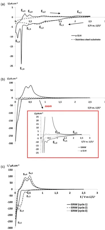
Fig. 1a shows the first CVs of a-Si:H thin film and stainless steel substrate performed in PC/LiClO4 1M. The differences between CVs for stainless steel and a-Si:H electrodes give evidence of the Li–Si alloying reactions occurring with Si thin film electrodes. The CV
Fig. 1. Cyclic voltamperogram in PC/LiClO4 (1 M) at 20 /LV s1 on (a) a thin amor- phous film of a-Si:H and stainless steel substrate; (b) Si nanowires (SiNW) and a thin amorphous film of a-Si:H; (c) three first cycles (CV) on Si nanowires (SiNW).
of stainless steel and a-Si:H thin film electrode (Fig. 1a) shows two broad cathodic peaks Ec,1 and Ec,2 at 1.45 and 0.75 V, respec- tively. One small Ec,3 peak at around 0.45 V (not discussed) and two sharp and intense peaks located at 0.2 and 0.1 V (Ec,4 and Ec,5 , respectively) are only observed on a-Si:H films. The first cathodic peak (Ec,1 ) can be attributed to small-scale reduction of electrolyte and/or surface contaminations (including silicon oxide) on Si elec- trodes [25]. A reduction of trace of water (30 ppm) present in the electrolyte cannot be completely excluded as already discussed in previous studies on PC/Li salts electrochemical reduction per- formed on noble metals [30–32]. Ec,2 peak present at 0.75 V is a principal peak attributed to reduction of the electrolyte on Si electrodes [11,12,24–26]. The very sharp Ec,4 and the Ec,5 peaks may correspond to the lithiation of amorphous Si, which have been reported to occur below 200 mV [13,33]. Two features were observed during lithiation of amorphous Si. It can be concluded that Ec,5 and Ec,4 peaks are related to formation of amorphous Li–Si phase, since they are not observed on the CV performed on stain- less steel. The Ec,5 value has been observed in both crystallised and amorphous Si [35]. During the Li–Si de-alloying reactions, two anodic peaks (Ea,5 and Ea,4 , respectively, Fig. 1a) are observed at 0.36 and 0.52 V, as it was reported in the literature for amorphous Si and thin Si films [34,35]. These two anodic peaks seem to cor- respond to de-alloying of amorphous Li–Si phase as they are not present on the CV performed on the stainless steel substrate. These peaks are characteristic of the lithiation of amorphous Si and thin Si films [36–38]. The sharp nature of Ec,4 peak is rather surprising, indicating a possibility of other processes related to the presence of H-atoms in a-Si:H film. The small and broad anodic peaks, Ea,2 and Ea,1 located at 0.93 and 2.00 V are related to oxidation reaction of compounds reduced at cathodic process (peaks Ec,1 and Ec,2 , Fig. 1a) on both stainless steel and a-Si:H thin film. Fig. 1b shows cyclic voltammetry performed on the SiNW electrode in PC/LiClO4 1M. The same cathodic peaks (Ec,1 , Ec,2 , Ec,3 and Ec,4 ) corresponding to the same electrochemical reactions occurring on a-Si:H electrodes (Fig. 1a) are observed for SiNW (Fig. 1b). The Ec,1 , Ec,2 and Ec,3 peaks related to electrochemical reactions occurring on the electrode sur- face are almost undetectable on the CV performed on the SiNW electrode. It can be noticed that in a case of the CV performed on the SiNW electrode the peak Ec,4 (very well visible on the a- Si:H electrode, Fig. 1a) appears as a shoulder before the peak Ec,5 (Fig. 1b). The peak Ec,4 is attributed to lithiation of a small amount of amorphous Si present in crystalline SiNW, while the peak Ec,5 (<100 mV) is mainly attributed to lithiation of crystalline Si (present in SiNW), formation of amorphous Li–Si phase (a-Lix Si) and/or crys- tallisation to Li15 Si4 phase at potentials lower than 50 mV [7,34]. De-alloying of amorphous Li–Si phase occurs during the reverse cycle at the same potentials (Ea,5 and Ea,4 in Fig. 1b) as for a-Si:H (Ea,5 and Ea,4 in Fig. 1a). The two de-alloying peaks clearly seem to suggest that there is no crystallisation of a-Lix Si onto Li15 Si4 (c- Li15 Si4 ). These results are consistent with previous findings and can be related to nano-sized morphology of SiNW [39]. If c-Li15 Si4 was formed a single de-lithiation peak characteristic of a two- phase region (c-Li15 Si4 and a-Si) should be observed [34]. In a case of CV performed on SiNW the peaks Ea,5 and Ea,4 are char- acterised by high current density (high charge) due to high specific area of SiNW electrode. The analysis of second and third cycles (Fig. 1c) clearly shows an intensity increase of the E4,c peak and a decrease of the Ec,5 peak with cycling. The Ec,4 peak displaces to much higher potentials indicating that the lithiation of amorphous Si is easier than lithiation of crystalline Si. These findings are in agreement with conversion of crystalline Si to amorphous Si dur- ing lithiation process [34]. Recent NMR studies have demonstrated that during the first lithiation the Si matrix breaks down to form amorphous Si matrix which can be lithiated at lower overpotentials
3.2. Morphological characterisation
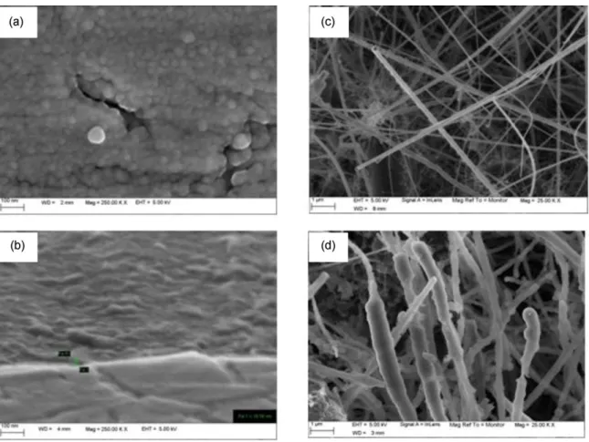
Fig. 2a and b show SEM micrographs of a-Si:H film before and after cycling (1CV). Before cycling, the a-Si:H film exhibits a pearl- bead structure, whereas after one complete cycle in PC/LiClO4 1M, it is covered by a thin, relatively homogenous and smooth-like film, which may indicate the presence of a SEI layer. Fig. 2c and d represent FEG-SEM micrographs of SiNW electrode before and after one cycle (CV). On the pristine SiNW electrode, nanowires appear regular-in-shape, whereas on the cycled SiNW electrode the nanowires are considerably thicker and covered with the SEI layer. The formation of the SEI layer all along each silicon nanowire confirms the good electrolyte diffusion in depth of the porous SiNW electrode. A significant modification of the a-Si:H and SiNW elec- trode related principally to full surface coverage by the SEI layer is confirmed by the electrochemical results as well as the XPS and ToF-SIMS analyses (vide infra).
3.3. XPS characterisation of pristine and (de)lithiated silicon electrodes
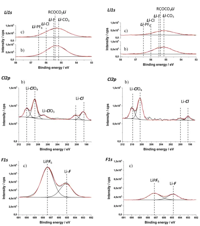
Fig. 3 presents the XP spectra of C 1s, O 1s and Si 2p core lev- els recorded for the pristine (a) and the cycled (1CV) a-Si:H and SiNW electrodes in PC/LiClO4 1M (b) and in EC:DMC (1:1)/LiPF6 1 M (c). Fig. 4 shows the Li 1s, F 1s and Cl 2p core level spectra of a-Si:H and SiNW samples cycled in PC- (Fig. 4a) and EC:DMC-based electrolytes (Fig. 4b). The XP spectra for pristine a-Si:H and SiNW electrodes were corrected by 1.2 eV and 1.0 eV, respectively, with respect to C 1s reference (285.0 eV).
Fig. 3a displays Si 2p3/2 (EB = 99.3 eV, FWHM = 0.7 eV) and Si 2p1/2 (EB = 98.7 eV, FWHM = 0.7 eV) spin orbit doublet assigned to silicon (Si0 ) and non-deconvoluted Si 2p (E
B = 102.6 eV, FWHM = 1.7 eV) attributed to the native silicon oxide (SiO2 ). The pristine SiNWs (Fig. 3a, Table 3) shows, similarly to the a-Si:H film, a Si 2p3/2 doublet and a non-deconvoluted Si 2p at higher binding energy attributed to Si0 and SiO
2 , respectively. The slightly larger FWHM values of Si 2p peaks for SiNW electrode (FWHM = 0.9 for Si0 and FWHM = 2.2 eV for SiO2 ) can be related to different surface mor- phology (i.e. increased roughness of Si wire-like structure). The thickness of the native SiO2 formed on the SiNW calculated from Eq.
(1) is around 1 nm. However, this value can be only an approximate estimation, since Eq. (1) is only valid for planar surfaces. Moreover, Si 2p(Si0 )/Si 2p(SiOx ) intensity ratio was estimated to be equal to 5.7 and 1.7 for a-Si:H thin film and SiNW electrodes, respectively (Fig. 3a), indicating that the surface of SiNW electrode is more oxi- dised, which can be due to high surface area of SiNW. O 1s peak displayed at EB = 532.3 eV (FWHM = 1.7 eV) for a-Si:H thin films and at EB = 532.6 eV (FWHM = 1.7 eV) for SiNW samples (Fig. 3a) con- firms the presence of a native SiO2 on the electrode surface. The oxygen to silicon intensity peaks ratios (O 1s(SiOx )/Si 2p(SiOx )) are 1.75 and 2.96 for SiNW and a-Si:H pristine samples, respectively. The slightly higher O 1s/Si 2p atomic intensity ratio found in a- Si H with respect to the theoretical value ([O 1s/Si 2p]th = 2), can be related to presence of oxygenated carbon species (contamina- tion including C O or O C O bonds). Indeed, the presence of SiO2 , C O and/or O C O in a-Si:H films is confirmed by the O:Si:C ratio, which was found to be equal to 5:2:1 if all oxygenated species, i.e., oxygenated carbon and silicon oxide, were taken into account. In this case a O:Si ratio equal to 2 is calculated.
After a complete CV in PC- and EC:DMC-based electrolytes per- formed on both electrodes (a-Si:H thin film and SiNW) the XP spectra show strong attenuation and positive shift of Si 2p peaks (Fig. 3b and c). The displacement of Si 2p peak to higher binding energy (of around 2 eV) for the a-Si:H thin films, indicates strong modification of the electrode surface due to formation of the SEI layer which contributes to charging effect. The attenuation of the
Si 2p peaks is consistent with the growth of a SEI layer on the electrode surface. After correction of binding energies (BEs) of all spectra with reference to C 1s peak (285.0 eV), the Si 2p peaks are found at EB = 98.6 eV and 98.1 eV on the a-Si:H electrode cycled in PC and in EC:DMC-based electrolytes, respectively. The Si 2p signals (corresponding to Si0 and SiO2 ) are shifted to much lower BE values when comparing to pristine samples. The overcorrection of BEs of Si 2p core level peaks indicates that using the reference C 1s peak (at 285.0 eV) to adjust the values of binding energies is not appro- priate for all core level peaks. A discrepancy of binding energies of different components (core level peaks) can be influenced by differ- ent depth distribution of these components in analysed layer (SEI, SiO2 and/or Si layers). The correction of XP spectra with respect to Si 2p (99.3 eV) reference shifts the Si 2p peaks (corresponding to SiO2 ) back again to their expected values as observed on the pris- tine sample (EB = 102.4 and EB = 102.9 eV in PC- and EC:DMC-based electrolytes, respectively, Table 2). The same findings are observed on SiNWs cycled in PC- (Fig. 3b) and EC:DMC-based electrolytes (Fig. 3c) where correction of 2.3 eV and 2.1 eV, respectively, with respect to C 1s reference (at EB = 285.0 eV) leads to displacement of Si 2p peaks to much lower BEs (see Table 2).
Moreover for SiNW electrode cycled in PC compared to EC:DMC- based electrolytes show much stronger attenuation of the Si 2p peaks and higher charge effect indicating that a thicker SEI layer is formed (as discussed above). The XP spectra calibration with refer- ence to Si 2p (at EB = 99.3 eV) leads to displacement of C 1s and O 1s peak energies to much higher values, when calibration is done with C 1s reference (Table 2). However, the calibration of the XP spectra with the reference to Si 2p (99.3 eV) does neither allow to obtain the right binding energies of the compounds of the SEI layer. There- fore, it is suggested that the organic-part of the SEI layer is likely present at the outermost surface. Li 1s and F 1s peak energy values are much closer to compounds found on SEI layer of cycled graphite in EC:DMC/LiPF6 1M (Table 1), when Si 2p reference is used for BEs correction (Table 2).
While, on pristine samples the C 1s and the O 1s core level peaks are mostly attributed to traces of organic contaminations and native SiO2 on the electrode surface, after cycling the significant increase of the C 1s and O 1s peak intensities and the modifica- tions produced on the peak shapes indicate the presence of the SEI layer (Fig. 3b and c). If C 1s (285.0 eV) reference is used the C 1s core level can be decomposed in four components at 285.0, 286.8, 288.7 and 290.0 eV assigned to CH2 CH2 , C O, O C O and CO3 bonds, respectively, in the case of a-Si:H thin films cycled in PC-based electrolyte (Fig. 3b). Similar values (peaks at 285.0, 287.0, 288.8 and 290.1 eV) are found when the a-Si:H electrode is cycled in EC:DMC-based electrolyte (Fig. 3c using C 1s reference). The new peak at 290.0 eV, assigned to carbon bonded to three oxy- gen atoms, is typical of carbonate-like species: Li2 CO3 (from DMC reduction), alkyl carbonates (ROCO2 Li with R CH3 , C2 H5 or C3 H7 arising from the electrochemical reduction of DMC, EC or PC) or semicarbonate species (R(OCO2)2 Li2 with R (CH2 )2 or CH3 (CH2 )2 originating from the electrochemical reduction of EC or PC) [41–45]. The inorganic Li2 CO3 and the organic ROCO2 Li and R(OCO2 )Li2 species can be distinguished by their C O bonding as the former contains a C atom attached to three O atoms, while the later has an additional R(C) O bond besides the carbon bonded to the three O atoms [41]. The CO3 peak is more intense for both electrodes (a-Si:H and SiNW) when the electrodes are cycled in PC- rather than EC:DMC-based electrolytes. The more intense C 1s peaks at 286.8/287.0 eV, assigned to C atom bonded to one O atom indicates the presence of lithium alkyl carbonates species (ROCO2 Li). The Li2 CO3 and ROCO2 Li compounds can be distinguished by precise analysis of O 1s spectra, where in the presence of ROCO2 Li species the O 1s is slightly asymmetric [41]. For the a-Si:H electrode cycled in PC-based electrolyte, the O 1s core level spectrum corrected with
Fig. 2. FEG-SEM micrographs of (a) pristine thin film a-Si:H and (c) pristine Si nanowires (SiNW) and after one CV in PC/LiClO4 1M performed on (b) a-Si:H thin film and (d) SiNW.
Table 1
XPS peak assignments of SEI layer compounds according to the literature.
Compound Si 2p (eV) C 1s (eV) O 1s (eV) Li 1s (eV) Cl 2p (eV) F 1s (eV)
SiO2 103.3c Si0 99.3c Hydrocarbons 285 284.8e Polymer 285.5–286.5 PEO (C O) 286.5d , e 533e Li2 CO3 291.5b , e 533.5–534b , e 56.5b 290.1a 531.8a 55.5a 290.0c , d 55.2c R CH2 OCO2 Li 290.1a 531.8a 289–290e 532.2e R CH2 OCO2 Li 286.5a 533.3a 55.5a 288.0d 287.5–288e R CH2 OCO2 Li 285.3a R CH2 OLi 286.5d Li F 56.2–56.6b , e 686–686.5b , e 55.6c 685.5c Li Cl 198.5g Li ClO4
Li–PF6 /Lix PFy 57b 688b , e
56.6c Li Si 98d 98.4c Li OH 530f Li2 O 530f a Ref.
[41] for ROCO2 Li species calibrated to C 1s (285.0 eV).
b Ref. [64] for SEI/graphite calibrated to C 1s (284.4 eV or 286.7 eV, in the presence of carbon black or not respectively). c Ref. [19] for SEI/a-Si:H calibrated to C 1s (285.0 eV).
d
Ref. [11] for SEI/SiNW calibrated to C 1s (284.5 eV). e Ref. [48] for SEI/graphite calibrated to C 1s (284.3 eV).
f Ref. [65] for SEI/graphite calibrated to C 1s (284.5 eV) of graphite or C 1s (285.9 eV) in the absence of graphite. g Ref. [45,51].
Fig. 3. XPS high resolution spectra of Si 2p, C 1s, O 1s for (a) pristine a-Si:H thin film and SiNW and cycled (1CV) thin film a-Si:H and SiNW in (b) PC/LiClO4 1M and (c) EC:DMC (1:1) (wt/wt)/LiPF6 1M. The binding energies of all spectra were corrected with respect to C 1s reference at 285.0 eV.
respect to C 1s reference can be decomposed into three major com- ponents located at 533.9, 532.0 and 530.1 eV which can be assigned to alkyl chain (RCH2 ) bonded to an oxygen atom of a CO3 group [RCH2 O CO2 bond], O C O bonds in CO3 and to OH or OR, respectively [44,46–50]. No significant changes are observed in O 1s peaks binding energies for the a-Si:H electrode cycled in EC:DMC- based electrolyte (Table 2). The O 1s spectrum for the SiNW samples cycled in PC-based electrolyte shows also three major components at 533.6, 532.0 and 530.3 eV. When replacing the electrolyte by EC:DMC, only small changes in the values of binding energies are observed, similarly to a-Si:H sample (Table 2). The peak around
532.0 eV is assigned to O C O bond in CO3 , which is related to the formation of Li2 CO3 or alkyl carbonate species, in agree- ment with the increase of C 1s peak intensity at 290.1/290.2 eV. The peak at 533.6/533.7 eV is assigned to alkyl side chain (RCH2 ) attached to CO3 [41], in agreement with the C 1s peak at 286.7 eV attributed to C O bound found in RCH2 OCO3 compounds (Table 1), while peak at 530.3 can be related to ROLi species originating from DMC reduction [25] or LiOH from trace water reduction [30,31]
The SiNW samples cycled in EC:DMC- show a stronger OH/RO contribution in the O 1s core level peak than samples cycled in PC- based electrolyte. This can be related to formation of ROLi due to
Fig. 4. XPS high resolution spectra of Li 1s, Cl 2p and F 1s for (a) pristine a-Si:H thin film and SiNW and cycled (1CV) thin film a-Si:H and SiNW in (b) PC/LiClO4 1M and (c) EC:DMC (1:1) (wt/wt)/LiPF6 1M. The binding energies of all spectra were corrected with respect to C 1s reference at 285.0 eV.
reduction of DMC. The contribution of OH/RO is not as signif- icant as the contribution of alkyl carbonates and Li2 CO3 in the composition of the SEI layer.
Salt decomposition (reduction) products were identified from Li 1s, F 1s and Cl 2p peak analysis (Fig. 4). Both a-Si:H and SiNW samples cycled in PC- (Fig. 4a) and EC:DMC-based (Fig. 4b) elec- trolytes have rather high lithium content (~25% at.) after one complete cycle. As the Li 1s peak is symmetrical and centred at 55.2 eV (FWHM ~1.6 eV), no attempt was made to assign precisely Li-containing species from Li 1s core level spectra deconvolution. The Li 1s at binding energy of 55.2 eV can be attributed to Li2 CO3 and lithium alkyl carbonate species (ROCO2 Li) [41,45]. For a- Si:H and SiNWs cycled in electrolytes containing LiClO4 salt, LiCl
(56 eV) is observed in the SEI layer as confirmed by the appear- ance of a Cl 2p3/2 and Cl 2p1/2 peaks at around 200.2/200.0 eV and 198.6/198.4 eV, respectively, while LiClO4 salt contamina- tion was confirmed by Cl 2p3/2 and Cl 2p1/2 peaks appearing at 210.0 and 208.4 eV, respectively [51]. The assessment of the con- tribution of LiClO4 to the Li1s core level peak is difficult as no reference data can be found in the literature. For samples cycled in electrolytes containing the LiPF6 salts, the Li 1s peak includes contributions from LiF (from 56.6 to 55.6 eV) and LiPF6 (or Lix PFy species) (from 57 to 56.5 eV) [45] (Table 1) originating from salt reduction/decomposition reactions and salt contamination. The quantitative analysis of F 1s/P 2p ratio equal to 6 indicates the presence of LiPF6 compounds (Table 3).
Si C O Li Cl F P nals, respectively, was used as criterion. These regions are defined
PC-based electrolyte 1.4 36.1 39.0 22.6 1.0 – – in ToF-SIMS figures (Figs. 5 and 6) with vertical dashed lines.
EC:DMC-based electrolyte 17.3 30.0 34.4 16.0 – 2.4 ever, the use of this criterion shows its limit in pristine (Fig. 5a) and
Table 2
Binding energies values for silicon samples cycled in PC/LiClO4 1M (PC) and EC:DMC(1:1)/LiPF6 1M with two different references for the charge correction (C 1s and Si 2p).
Sample C 1s (eV)
O 1s (eV)
Si 2p (eV) Li 1s (eV) F 1s (eV)
Cl 2p (eV)
a-Si:H
Pristine 285 531.3 98.7 286.7 532.3 99.3 288.7 533.9 102.6 289.6 PC 285.0a 285.7b 533.9a 534.7b 98.6a 99.3b 55.2a 56.0b
210.0a 211.0b 286.8a 287.5b 532.0a 532.8b 101.6a 102.4b 208.4a 209.4b
288.7a 290.0a 289.4b 290.7b 530.1a 530.9b
200.2a 198.6a 201.0b 199.4b EC:DMC 285.0a 286.2b 533.9a 535.1b 98.1 a 99.3b 55.3a 56.5b 687.4a 688.6b
287.0a 288.8a 290.1a 288.2b 290.0b 291.3b 532.1a 530.6a 533.3b 531.7b 101.7a 102.9b 685.1a 686.3b
SiNW
Pristine 285 533.9 98.7 286.7 532.5 99.5 102.7 PC 285.0a 286.3b 533.6a 534.9b 98.0a 99.3b 55.2a 56.5b
210.0a 211.3b 286.7a 288.0b 532.0a 533.3b 101.4a 102.7b 208.4a 209.7b
288.8a 290.1a 290.1b 291.4b 530.3a 531.6b
200.0a 198.4a 201.3b 199.7b EC:DMC 285.0a 286.2b 533.7a 534.9b 98.1 a 99.3b 55.1a 56.3b 687.2a 688.4b
286.7a 288.7a 290.2a 287.9b 289.9b 291.2b 532.0a 530.5a 533.2b 531.7b 101.7a 102.9b 684.9a 687.1b
a C 1s (285.0 eV).
b Si 2p (99.3 eV) charge effects correction.
Table 3
Surface composition (atomic percentage) for cycled a-Si:H thin film electrodes mea- sured by XPS.
Li = 25% and 16% for the a-Si:H thin film and the SiNWs, respec- tively. These values are close to the atomic percentages reported
for Si cycled in EC:DMC-based electrolytes [20], where the SEI
Si C O Li Cl F P PC-based electrolyte 2.2 30.0 47.4 19.8 0.6 – – EC:DMC-based electrolyte 4.1 25.6 35.7 25.2 – 6.8 9.4
From the F 1s core level analysis, a peak at 687.4/687.2 eV and at
685.1/684.9 eV corresponding to LiPF6 and LiF species [11], respec-
tively, was found on the a-Si:H and SiNW cycled in EC:DMC-based electrolyte (Fig. 4a). The values of BEs of these two peaks are lower by about 0.5–1 eV than the values reported in the literature for LiF (686–686.5 eV) and LiPF6 (688.0 eV) [52–54]. After charge correc- tion made with reference to the Si 2p core level peak, the binding energies of LiPF6 and LiF are in agreement with those reported in the literature, e.g. 688.6/688.4 and 686.3/687 eV, respectively (Table 2). The charge correction vs Si 2p shifts also the Li1s peak to 56.5/56.3 eV, which can be assigned to the presence of LiF [50,64].
Tables 3 and 4 show atomic percentage of the elements found in a-Si:H and SiNW samples, respectively, after one complete CV. Both Si electrode samples (a-Si:H and SiNWs) have higher content of C, O and Li species when cycled in PC- than in EC:DMC-based elec- trolytes. The atomic percentage values found for samples cycled in EC:DMC-based electrolytes are: C ~= 26% and 30%, O = 36% and 34%,
Table 4
Surface composition (atomic percentage) of the SiNW electrodes measured by XPS.
layer was suggested to be oxygen-rich in contrast to Si cycled in fluoro-ethylene carbonate (FEC)-based electrolytes [20]. The atomic percentage of oxygen in the SEI layer formed on the a- Si:H thin film and the SiNWs after cycling in PC-based electrolyte is higher that those obtained in EC-DMC electrolyte (Tables 3 and 4). As shown from the XPS depth profiles by Nakai et al. [20] the SEI layer grown on the Si film electrode cycled in EC-based electrolyte containing LiPF6 was thicker than those formed in FEC-based elec- trolytes containing LiPF6 salt, due to formation of fluoride ions from the solvent decomposition reactions in the latter case. Here, the growth of thicker SEI layer in the electrolyte free of fluorinated salts can be interpreted according to the same reasoning used for the mechanism of electrolyte reduction.
3.4. ToF-SIMS depth profile analyses of pristine and (de)lithiated silicon electrodes
ToF-SIMS ion-depth concentration profiles are collected from negative-ion mass spectra as a function of etching time. The inten- sity is reported using a logarithmic scale in order to magnify the low intensity signals. The variation of the ion intensity with sput- tering time reflects the variation of the in-depth concentration of the analysed ions but also the influence of the chemical envi- ronment on ionisation/emission yield of analysed species (called matrix effect). To define SiO2 , Si, substrate (SS) and SEI regions, 75% of the maximum intensity of SiO2 , Si3 , FeO2 and Li ion sig-
Fig. 5. Tof-SIMS depth profiles (negative ions) of (a) pristine a-Si:H thin film and
cycled a-Si:H in (b) PC/LiClO4 1M and in (c) EC:DMC (1:1)/LiPF6 1M.
cycled SiNW samples where the gap between SiO2 and Si metal regions (indicated by arrows in solid line) would suggest that no interface exists between Si and SiO2 regions. To take into account this difficulty associated to cycling resulted in increased rough- ness of the samples, dashed lines defining different regions were also traced. Although the limited usefulness of this criterion, we
Fig. 6. Tof-SIMS depth profiles (negative ions) of (a) pristine SiNW and cycled SiNW
in (b) PC/LiClO4 1M and in (c) EC:DMC (1:1)/LiPF6 1M.
have decided to keep it as a first approach to emphasise increased electrode roughness with cycling.
3.4.1. Pristine and (de)lithiated a-Si:H films
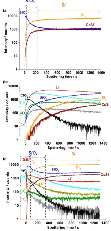
Fig. 5a shows the ToF-SIMS ion depth profiles of SiO2 , Si3 , Fe2 and FeO2 performed on pristine a-Si:H thin film (30 nm in thickness) deposited on a stainless steel substrate. Depth profiles of ions constituting the SEI layer (Li, CH2 , CO2 , CO3 , ClO4 , LiF and PF6 ) are also presented in Fig. 5b and 5c for a-Si:H thin films cycled in PC- and in EC:DMC- based electrolytes, respectively. Several regions can be identified on the a-Si:H pristine electrode (Fig. 5a). The very first seconds of sputtering are characterised by a very sharp increase for all ion sig- nals, which corresponds to the lapse of time needed to reach ion
sputtering stationary state. In the first ~20 s of etching, the SiO2 ion signal reaches its maximum marking the native silicon oxide region and then rapidly decreases at the maximum of Si3 ion signal. A stable Si3 signal is observed over ~800 s marking a homogenous, thin Si layer. The SiO2 signal becomes again more intense at the Si thin film (given by Si3 )/stainless steel (given by Fe2 and FeO2 ) interface, indicating the presence of SiO2 . The Fe2 and FeO2 signals are also observed from 0 s to 700 s sput- tering time but their intensity are rather low. The Fe2 and FeO2 signals observed from the beginning of sputtering originate from imperfections (like defects and pinholes) present in the a-Si:H films prepared by PVD [55–57]. Through the pinholes the primary ions can easily reach the exposed substrate surface (Fe2 and FeO2 sig- nals). However after 700 s of sputtering, the Fe2 and FeO2 signals become more intense. The maximum intensity of the Fe2 ion pro- file is stabilised near 1200 s, while that of FeO2 ion profile reaches a maximum near 950 s to thereafter slowly declines. Moreover, the FeO2 and the SiO2 ion profiles have similar behaviour at the sili- con/substrate interface. These results indicate that during the first stages of a-Si:H deposition, silicon oxide is formed, due to reaction of oxygen atoms, coming from the native oxide of the stainless steel substrate, with the newly formed hydrogenated amorphous silicon layer. The pristine a-Si:H electrode is characterised by a homoge- nous thin layer of silicon metal and the presence of silicon and iron oxides at the Si/substrate interface. The growth of a spuri- ous thermal oxide in the initial stages of the deposition process prior to complete sealing at the substrate surface can contribute to the interfacial oxides as previously observed at ALD layer/steel (or stainless steel) substrate interfaces [58–60].
Fig. 5b displays the depth profiles (negative ions) of a-Si:H after one complete CV (charge/discharge) in PC/LiClO4 (1M) at 20 /LV s1 , where some modifications can be observed. The first modification concerns the slight decrease in the sputtering time from 700 s to 600 s necessary to reach the interface silicon/stainless steel sub- strate which can indicate a contraction of amorphous silicon film after delithiation and/or structural damages of the a-Si:H film. Significant modifications can be observed in the Si3 profile: dis- placement of the etching time from 0 s to ~40 s; marked decrease in the Si3 signal intensity (from 20,000 to 5000 counts); and reduction of the sputtering time length from nearly ~800 s (before cycling) to ~500 s (after cycling). Changes are also observed on the SiO2 ion profile: decrease in the maximum signal intensity (from 20,000 to 9000 counts); and increase of the etching time length (from 20 s to ~150–110 s, given by dashed and solid arrows, respec- tively). The last modification concerns the appearance of new ions (Li, CH2 , CO2 , CO3 , ClO4 , LiF and PF6 ) in the depth pro- file (prior to the Fe2 signal), which correspond to the presence of the SEI layer (ions corresponding to decomposition products of the electrolyte). The difference between the beginning of the sputter- ing time and the appearance of the Fe2 signal could be used to estimate the SEI layer thickness.
A small intensity shoulder is observed in the Li ion profile before the maximum ion intensity is reached (~100 s) and then the Li declines to reach a minimum intensity near ~600 s. This two-step Li profile can be related to lithium ions being ionised from two different chemical environments: organic vs inorganic matrix and/or non-oxide/oxide environments, also called matrices, which affects lithium ionisation/emission yields. This two-step Li profile behaviour was already observed (but not discussed) in the ToF-SIMS ion profiles of de-lithiated thin film Cr2 O3 /Cr electrodes
[61]. This profile shape was not observed in de-lithiated tin alloys cycled in PC/LiClO4 1M (Sn–Co, Sn–Ni) [50,62]. Moreover, at the sil- icon/substrate interface the Li signal intensity increases again and follows SiO2 signal intensity. This can be due to enhanced ionisa- tion/emission of lithium ions in SiO2 (called matrix effect) or due to lithium trapped at the silicon/substrate interface. The irreversible
trapping of the lithium ions at the active material electrode thin film/metallic substrate interface after cycling was already observed in our previous studies [63]. It was shown that the quantity of lithium accumulated at the electrode thin film/substrate interface depends on the number of cycles (lithium insertion/de-insertion)
[63] and on electrode film/substrate cohesion. Lithium trapping had deleterious effect on cycling stability and capacity retention
[50,62,63].
A very intense ClO4 signal is observed at the first seconds of etching time and then it rapidly declines just before the maximum intensity of Li ion profile is reached, indicating that ClO4 is mainly due to salt contamination present on the electrode surface which were not completely removed with DMC solvent. The CH2 and CO3 ion profiles can indicate the presence of organic carbonate species in the SEI layer. Due to possible interferences in the mass spectra of certain ions having very close masses, two signals (CO3 and CO2 ) were used to probe carbonate species present in the SEI layer. The CO3 (mass 59.98) is difficult to be separated from SiO2 having a very similar mass (mass 59.96) and appears as a shoulder of the SiO2 peak (not shown here). Although very similar mass val- ues of CO2 and SiO signals (43.98 for CO2 and 43.97 for SiO), the peaks are clearly separated. Peak separation in mass spectra is improved for small mass values (in order to keep mass resolu- tion given by �M/M constant), thus the separation of CO2 and SiO is better than the SiO2 and CO3 mass peaks. Fig. 5b clearly shows that CO2 signal follows CO3 signal, indicating that there is no significant interference of SiO2 signal in CO3 depth profiles. Moreover, CH2 depth profile follows the CO3 and CO2 carbon- ate species profiles indicating that organic carbonate species are likely to be formed on the electrode surface, as already suggested by XPS analysis.
The Li–Si alloying/de-alloying reactions leading to Si structural changes are expected to occur independently of the nature of the electrolyte, contrary to the SEI layer for which the composition is highly dependent on solvent and salt nature. ToF-SIMS depth profiles of Si electrode cycled in EC:DMC (1:1)/LiPF6 1M clearly show that changing electrolyte has no incidence on the structure of cycled electrodes. The same structural modifications described for a-Si:H electrodes cycled in PC/LiClO4 1M are observed. Only attenuation of SiO2 maximum intensity is more significant in EC:DMC-based electrolyte (from 20,000 to 6000 counts), while SiO2 etching time length increases of the same amount (from 20 s (dashed arrow) to ~160–110 s (solid arrow). The ion pro- files corresponding to SEI layer species (Li, CH2 , CO2 , CO3 , LiF and PF6 ) started to be collected before Fe2 signal, indicat- ing that the electrode surface has been modified by the SEI layer. The Li ion profile (Fig. 5c) is quite similar to that observed on the Fig. 5b collected under the same operating conditions. A small shoulder of Li profile before reaching the maximum of the inten- sity for the a-Si:H cycled in EC:DMC-based electrolyte (Fig. 5c) is also observed as shown previously (Fig. 5b). The products of salt reduction and contamination given by the LiF and PF6 , respec- tively, are detected on the electrode surface. The PF6 maximum intensity is observed at the outer layer surface of the electrode and then it rapidly declines, showing that DMC used for sample rinsing was unable to remove completely the salt contamination. The LiF signal maximum intensity is reached at the maximum of the Li intensity (see black dashed arrow), indicating that LiF is closer to the silicon oxide/silicon interface (inner part of the SEI layer), while maximum intensity of the CO3 and CO2 ion profiles (carbonate species) appear in the same region as the Li shoulder (outer part of the SEI layer). Compared to the a-Si:H cycled in PC- based electrolyte (Fig. 5b), the ToF-SIMS ion profile performed on the a-Si:H electrode cycled in EC:DMC-based electrolyte (Fig. 5c) exhibits a lower intensity of carbonate (decrease from 2000 to 300 and from 400 to 60 counts for the CO3 and CO2 ions, respectively)
indicating lower concentration of carbonate species in the SEI layer.
3.4.2. Pristine and (de)lithiated SiNW
Fig. 6 shows ToF-SIMS depth profiles (negative ions: SiO2 , Si3 and CsSi) for pristine SiNWs deposited on TiN/Ti/stainless steel substrate. The depth profiles of ions characteristic of the SEI layer (Li, CH2 , CO2 , CO3 , ClO4 , LiF and PF6 ) are presented in
Fig. 6b and c for SiNW cycled in PC- and EC:DMC-based electrolytes, respectively.
Due to the high thickness of the SiNW layer grown on the stain- less steel substrate (30 /Lm), the sputtering was not performed through the whole thickness of the SiNW film (Fig. 6a). As afore- mentioned using 75% of the maximum intensity of the SiO2 and Si3 signals to define SiO2 and Si0 regions (see solid arrows) in pristine SiNW (Fig. 6a), results in the appearance of a gap between these two regions, because of increased roughness associated with wire-like structure. Moreover, the Si disordered wire-like structure (Fig. 2c) significantly affects the Si3 and SiO2 ion depth pro- files, as it will be described later. As previously observed in a-Si:H thin films, in the very first seconds of sputtering the SiO2 sig- nal intensity increases and reaches a maximum after ~20 s (10,000 counts), indicating that SiO2 is mainly present on the surface of Si nanowires. However in a case of the SiNW sample, during the fol- lowing seconds of sputtering the SiO2 profile smoothly declines to reach a plateau. After 300 s of sputtering time, the SiO2 and Si3 signals become parallel, indicating that the silicon oxide layer covers the Si nanowires all along their length (in the performed range of sputtered-layer thickness). This is in contrast to the a-Si:H thin film (Fig. 5a), where only the outer part of the Si film was covered by the native silicon oxide due to exposure to ambient air resulting in spontaneous oxidation. The Cs+ ions implanted in sil- icon during sputtering were also detected as a CsSi signal. When the SiO2 signal reaches its minimum value the CsSi signal reaches its maximum intensity and becomes parallel to the Si3 signal. This indicates that silicon oxide is mainly located onto the Si nanowire surface.
Fig. 6b shows ToF-SIMS negative ion depth profile of SiNWs after one complete CV in PC/LiClO4 1M at 20 /LV s1 , where two main modifications of the electrode can be observed. The first modifica- tion is in the shape of the SiO2 and Si3 signals and the second is related to the appearance of new compounds (Li, CH2 , CO2 , CO3 , ClO4 ) corresponding to the formation of the SEI layer. In contrast to the pristine SiNWs, the SiO2 and Si3 ion profiles in cycled SiNWs do not cross each other, which indicates that a thick SEI-layer covers the nanowires all along their length and SiO2 signal is always more intense than Si3 signal. Moreover, a very high intensity of the Li signal, as compared to the low intensity of the signals characteristic of SiNW region (SiO2 and Si3 pro- files), also indicates the presence of a thick SEI layer, which is in agreement with the SEM (Fig. 2d) and XPS results. Meanwhile, the Li ion profile reaches the maximum intensity after around ~400 s of sputtering and thereafter smoothly declines to the same inten- sity value as the SiO2 signal after 1400 s of sputtering. Thus, no characteristic features of the SEI as those of the cycled a-Si:H thin films (Fig. 5b) and attributed to “matrix effects”, can be observed in cycled SiNW. The high intensity Li signal confirms that the SEI layer extends all along the NW length.
As described before in Fig. 5b, a very intense ClO4 signal observed during the first few seconds of the sputtering indicates the presence of electrolyte contamination on the SiNW electrode surface, not completely removed by rinsing with DMC solvent. This result is in agreement with the XPS analyses where Cl contami- nation (signal in the Cl 2p spectrum) was found on the surface of SiNW after cycling (Fig. 4). In addition, the CO3 and CO2 sig- nals were used to probe carbonate species in the SEI layer. For the
cycled SiNWs, the CO2 signal (principally recorded for checking the CO3 signal reliability) becomes crucial, since charging effects are significant for SiNWs (mass peak broadening and lower mass resolution). In Fig. 6b the CO2 in-depth concentration profile fol- lows the CO3 signal, indicating no significant interference of the SiO2 and CO3 signals (having very similar masses as aforemen- tioned). During the first ~200 s of sputtering, both the CO3 and CO2 signals are much more intense than the SiO2 signal, indicat- ing the presence of a carbonate layer onto the SiNWs surface. The intensity of the CO3 signal is one order of magnitude lower than in cycled a-Si:H thin film. Both carbonate signals follow the Li profile. Moreover, the CH2 depth profile follows the Li, CO3 and CO2 ion profiles indicating that organic carbonate species are likely to be formed on the electrode surface, as already observed by XPS.
After one complete CV in EC:DMC-based electrolyte moderate changes are observed in the shape of the SiO2 and the Si3 ion profiles of the cycled SiNWs (Fig. 6c) compared to pristine SiNWs (Fig. 6a). The SiO2 signal reaches its maximum at ~30 s (8000 counts) compared to ~20 s (10,000 counts) for pristine SiNW. The Si3 signal remains almost unchanged after cycling, indicating that a very thin SEI layer is formed on the SiNWs surface. The intensi- ties of the Li, CO3 and CO2 signals corresponding to products of electrolyte decomposition (SEI layer) are lower than for the SiNWs cycled in PC/LiClO4 1M, indicating the formation of a thinner SEI layer. Meanwhile, the intersection between the SiO2 and Si3 signals is observed at slightly longer etching times (100 s) as com- pared to pristine SiNW (120 s), confirming the formation of a thin SEI layer, in contrast with the thick SEI layer formed on the SiNW electrode after cycling in PC-based electrolyte. Following the PF6 signal (indicator of the level of contamination by salt after cycling) it can be concluded that this inorganic contamination is mainly observed at the extreme surface of SiNWs electrodes.
According to the ToF-SIMS results, a thicker SEI layer is formed on the surface of SiNW electrode after cycling (1CV) in PC/LiClO4 1 M than in EC:DMC (1:1)/LiPF6 1M electrolyte, independently of the degree of crystallisation and morphology of silicon electrodes (crystalline SiNW or a-Si:H thin films). The amount of carbonate at the silicon thin film surface is higher after cycling in PC/LiClO4 1M.
4. Conclusions
After one complete CV a full coverage SEI layer was formed on a- Si:H and SiNW surfaces using two distinct electrolytes (PC/LiClO4 1M and EC:DMC/LiPF6 1M). SEI presence was confirmed by XPS analysis, where an increase in the C 1s and O 1s intensity sig- nals and an appearance of new peaks associated with electrolyte reduction (Li 1s, F 1s, P 2p and Cl 2p) were observed. Furthermore, strong attenuation of Si 2p signal and displacement of XP spectra to higher energies related to charge effects confirms the presence of a SEI layer. SEM micrographs showed also modification of the electrode surface morphology. The use of C 1s or Si 2p references to correct charge effects allowed to conclude that the organic part of the SEI layer is present at the outermost surface. XPS analysis also showed that the organic, outer-part of SEI-layer formed in PC- based electrolytes is thicker and richer in alkyl carbonate species, than that formed in EC:DMC-based electrolytes. Inorganic outer- most part of SEI is mainly composed of salt decomposition products (LiCl or LiF) and LiClO4 or LiPF6 salt contamination not completely removed from electrode surface in washing process. These findings were confirmed by ToF-SIMS analysis, where a two-step lithium profile (Li ions) suggesting the presence of organic (in the outer surface) and inorganic (in the inner part of the layer) compound- layer in the SEI layer was observed. This distribution of organic and inorganic parts in the SEI layer is also confirmed by the CO2 and LiF signals, respectively. Furthermore, we have confirmed that Si
electrode morphology greatly influences ToF-SIMS depth profile, making data interpretation difficult in a case of the SiNW electrode. From this point of view the comparative study with Si planar elec- trode (a-Si:H) is very valuable to unravel the electrode/electrolyte interphase reactions taking place on SiNW surface. One can con- clude that XPS and ToF-SIMS techniques can be successfully applied to detect and study the SEI layer on complex structures (SiNW) by using planar surface models.
Acknowledgments
The work was partially funded by Renault. Région Ile–de–France is acknowledged for partial support for the XPS and ToF–SIMS equipment.
The authors thank Sandrine Zanna and Antoine Seyeux from Chimie Paristech (LPCS) for the analyses and useful discussions about XPS and ToF-SIMS results, and Stephan Borensztajn from Lab- oratoire Interfaces et Systemes Electrochimiques (Université Pierre et Marie Curie) for the SEM and EDX analyses.
The authors are grateful to Anna Teyssot and Christophe Dudez- ert from Renault for fruitful discussions.
References
[1] R.A. Hugging, Journal of Power Sources 81–82 (1999) 13.
[2] D. Larcher, S. Beattie, M. Morcrette, K. Edström, J.-C. Jumas, J.-M. Tarascon, Journal of Materials Chemistry 17 (2007) 3759.
[3] H. Okamoto, Journal of Phase Equilibria and Diffusion 30 (1) (2009) 118. [4] L. Tirado, Materials Science and Engineering R 40 (2003) 103.
[5] P. Limthongkul, Y.-I. Jang, N.J. Dudney, Y.-M. Chiang, Journal of Power Sources 119–121 (2003) 604.
[6] M.N. Obrovac, L. Christensen, Electrochemical and Solid-State Letters 7 (5) (2004) A93.
[7] T.D. Hatchard, J.R. Dahn, Journal of The Electrochemical Society 151 (6) (2004) A838.
[8] J. Li, J.R. Dahn, Journal of The Electrochemical Society 154 (3) (2004) A156. [9] W.J. Zhang, Journal of Power Sources 196 (2011) 877.
[10] C.K. Chan, H. Peng, G. Liu, K. McIlwrath, X.F. Zang, Y. Cui, Nature Nanotechnology 3 (2008) 31.
[11] C.K. Chan, R. Ruffo, S.S. Hong, Y. Cui, Journal of Power Sources 189 (2009) 1132. [12] C.K. Chan, R. Ruffo, S.S. Hong, R. Huggins, Y. Cui, Journal of Power Sources 189
(2009) 34.
[13] B. Laïk, D. Ung, A. Caillard, C.-S. Cojocaru, D. Pribat, J.-P. Pereira-Ramos, Journal of Solid State Electrochemistry 14 (2010) 1835.
[14] J.H. Ryu, J.W. Kim, Y.-E. Sung, S.M. Oh, Electrochemical and Solid-State Letters 7 (7) (2004) A306.
[15] A. Chagnes, J. Swiatowska, Lithium Ion Batteries - New Developments INTECH, in: I. Belharouak (Ed.), Electrolyte and solid-electrolyte interphase layer in lithium-ion batteries, 2012, pp. 145–172.
[16] I. Geoffroy, A. Chagnes, B. Carré, D. Lemordant, P. Biensan, S. Herreyre, Journal of Power Sources 112 (1) (2002) 191.
[17] A. Chagnes, B. Carré, P. Willmann, R. Dedryvère, D. Gonbeau, D. Lemordant, Journal of The Electrochemical Society 159 (9) (2003) A1255.
[18] P.B. Balbuena, Y. Wang, Lithium-Ion Batteries Solid Electrolyte Interphase, Imperial College Press, London, 2004.
[19] Y.M. Lee, J.Y. Lee, H.-T. Shim, J.K. Lee, J.-K. Park, Journal of The Electrochemical Society 154 (6) (2007) A515.
[20] H. Nakai, T. Kubota, A. Kita, A. Kawadhima, Journal of The Electrochemical Society 158 (7) (2011) A798.
[21] W. Xu, S. Sai, S. Vegunta, J.C. Flake, Journal of Power Sources 196 (2011) 8583. [22] Y.-C. Yen, S.-C. Chao, H.-C. Wu, N.-L. Wu, Journal of The Electrochemical Society
156 (2) (2009) A95.
[23] C. Cuong Nguyen, S.-W. Song, Electrochemistry Communications 12 (2010) 1593.
[24] B. Philippe, R. Dedryvere, J. Allouche, F. Lindgren, M. Gorgoi, H. Rensmo, D. Gonbeau, K. Edström, Chemistry of Materials 24 (2012) 1107.
[25] V. Etacheri, O. Haik, Y. Goffer, G.A. Roberts, I.C. Stefan, R. Fasching, D. Aurbach, Langmuir 28 (2012) 965.
[26] C.C. Nguyen, S.-W. Song, Electrochimica Acta 55 (2010) 3026. [27] H. Usui, Y. Kiri, H. Sakaguchi, Thin Solid Films 520 (23) (2012) 7006.
[28] J. S´ wiatowska-Mrowiecka, V. Maurice, S. Zanna, L. Klein, P. Marcus, Electrochi- mica Acta 52 (2007) 5644.
[29] S. Tanuma, C.J. Powell, D.R. Penn, Surface and Interface Analysis 20 (1993) 77.
[30] D. Aurbach, M. Daroux, P. Faguy, E. Yeager, Journal of Electroanalytical Chem- istry 297 (1991) 225.
[31] D. Aurbach, Y. Talyosef, B. Markovsky, E. Markevich, E. Zinigrad, L. Asraf, J.S. Gnanaraj, H.–J. Kim, Electrochimica Acta 50 (2004) 247.
[32] P.B. Balbuena, Y. Wang, Lithium-Ion Batteries: Solid-Electrolyte Interphase, Imperial College Press, London, 2004, pp. 91.
[33] L.-F. Cui, R. Ruffo, C.K. Chan, H. Peng, Y. Cui, Nano Letters 9 (2009) 491. [34] M.N. Obrovac, L.J. Krause, Journal of The Electrochemical Society 154 (2) (2007)
A103.
[35] L.B. Chen, J.Y. Xie, H.C. Yu, T.H. Wang, Journal of Applied Electrochemistry 39 (2009) 1157.
[36] M. Green, E. Fielder, B. Scrosati, M. Wachtler, J.S. Moreno, Electrochemical and Solid-State Letters 6 (5) (2003) A75.
[37] L.B. Chen, J.Y. Xie, H.C. Yu, T.H. Wang, Journal of Applied Electrochemistry 39 (2009) 1157–1162.
[38] V. Baranchugov, E. Markevich, E. Pollak, G. Salitra, D. Aurbach, Electrochemistry Communications 9 (2007) 796.
[39] C.K. Chan, R. Ruffo, S.S. Hong, R.A. Huggins, Y. Cui, Journal of Power Sources 189 (2009) 34.
[40] B. Key, M. Morcrette, J.-M. Tarascon, C.P. Grey, Journal of The American Chemical Society 133 (2011) 503.
[41] R. Dedryvère, L. Gireaud, S. Grugeon, S. Laruelle, J.-M. Tarascon, D. Gonbeau, Journal of Physical Chemistry B 109 (2005) 15868.
[42] M. Herstedt, A.M. Andersson, H. Rensmo, H. Siegbahn, K. Edström, Electrochi- mica Acta 49 (2004) 4939.
[43] S. Laruelle, S. Pilard, P. Guenot, S. Grugeon, J.-M. Tarascon, Journal of The Elec- trochemical Society 151 (2004) A1202.
[44] J. S´ wiatowska, V. Lair, C. Pereira-Nabais, G. Cote, P. Marcus, A. Chagnes, Applied Surface Science 257 (2011) 9110.
[45] P. Verma, P. Maire, P. Novák, Electrochimica Acta 55 (22) (2010) 6332. [46] E. Peled, D. Bar Tow, A. Merson, A. Gladkich, L. Burstein, D. Golodnitsky, Journal
of Power Sources 97–98 (2001) 52.
[47] R. Fong, U. Vonsacken, J.R. Dahn, Journal of The Electrochemical Society 137 (1990) 2009.
[48] A.M. Andersson, K. Edström, Journal of The Electrochemical Society 148 (2001) A1100.
[49] J.-T. Li, J. S´ wiatowska, A. Seyeux, L. Huang, V. Maurice, S.-G. Sun, P. Marcus, Journal of Power Sources 195 (2010) 8251.
[50] J.-T. Li, J. S´ wiatowska, V. Maurice, A. Seyeux, L. Huang, S.-G. Sun, P. Marcus, Journal of Physical Chemistry C 115 (2011) 7012.
[51] J.F. Moulder, W.F. Stickle, P.E. Sobol, K.D. Bomben, Handbook of X-ray Photo- electron Spectroscopy, Perkin-Elmer Corp, Eden Prairie, MN, 1992.
[52] D. Aurbach, Nonaqueous Electrochemistry, Marcel Dekker Inc., New York, 1999. [53] D. Aurbach, A. Zaban, Y. Gofer, Y. Ein Eli, I. Weissman, O. Chusid, O. Abramson,
Journal of Power Sources 54 (1995) 76.
[54] K. Kanamura, S. Shiraishi, H. Tamura, Z.-I. Takehara, Journal of The Electrochem- ical Society 141 (1994) 2379.
[55] P.M. Natishan, E. McCafferty, P.R. Puckett, S. Michel, Corrosion Science 38 (1996) 1043.
[56] P. Panjan, M. Cekada, M. Panjan, D. Kek-Merl, Vacuum 84 (2010) 209. [57] B. Díaz, J. S´ wiatowska, V. Maurice, M. Pisarek, A. Seyeux, S. Zanna, S. Tervakan-
gas, J. Kohlemainen, P. Marcus, Surface and Coatings Technology 206 (19–20) (2012) 3903.
[58] B. Díaz, J. S´ wiatowska, V. Maurice, A. Seyeux, B. Normand, E. Härkönen, M. Ritala, P. Marcus, Electrochimica Acta 56 (2011) 10516.
[59] B. Díaz, E. Härkönen, J. S´ wiatowska, V. Maurice, A. Seyeux, P. Marcus, M. Ritala, Corrosion Science 53 (2011) 2168.
[60] B. Díaz, E. Härkönen, V. Maurice, J. S´ wiatowska, A. Seyeux, M. Ritala, P. Marcus, Electrochimica Acta 56 (26) (2011) 9609.
[61] J.-T. Li, V. Maurice, J. S´ wiatowska-Mrowiecka, A. Seyeux, S. Zanna, L. Klein, S.-G. Sun, P. Marcus, Electrochimica Acta 54 (2009) 3700.
[62] J.-T. Li, J. Swiatowska, A. Seyeux, L. Huang, V. Maurice, S.-G. Sun, P. Marcus, Journal of Power Sources 195 (2010) 8251.
[63] J. S´ wiatowska-Mrowiecka, F. Martin, V. Maurice, S. Zanna, L. Klein, J. Castle, P. Marcus, Electrochimica Acta 58 (2008) 4257.
[64] H. Bryngelsson, M. Sjterndahl, T. Gustafsson, K. Edström, Journal of Power Sources 174 (2007) 970.
[65] M. Herstedt, D.P. Abraham, J.B. Kerr, K. Edström, Electrochimica Acta 49 (2004) 5097.