DOCTEUR DE L’UNIVERSITE DE POITIERS
Faculté des Sciences Fondamentales et AppliquéesDiplôme National - Arrêté du 7 Août 2006
ÉCOLE DOCTORALE SCIENCES POUR L’INGENIEUR & AERONAUTIQUE
DOMAINE DE RECHERCHE : MILIEUX DENSES, MATERIAUX ET COMPOSANTS
Présentée par
Vivek Vishwanath Antad
Contrôle de la croissance et de la réactivité
de nanoparticules métalliques par spectroscopie
optique
in situ
Directeur de thèse: D. BabonneauCo-direction: L. Simonot Soutenue le 3 novembre 2011 Devant la Commission d’Examen
JURY
Y. Borensztein Directeur de Recherche au CNRS, INSP, Paris Rapporteur M.-C. Saint-Lager Directeur de Recherche au CNRS, INEEL, Grenoble Rapporteur N. Destouches Professeur d’Université, LHC, Saint-Etienne Examinateur G. Abadias Professeur d’Université, Institut Pprime, Poitiers Examinateur D. Babonneau Chargé de Recherche au CNRS, Institut Pprime, Poitiers Examinateur L. Simonot Maître de Conférence, Institut Pprime, Poitiers Examinateur
The work penned in this Ph.D. manuscript is a yield of three-year research that I have carried out in the research group “Nanoparticules et Nanostructures” from “Département de Physique et Mécaniques des Matériaux” of “Institut Pprime” within the “Université de Poitiers”.
As is always the case, completion of such a profound research work contains numerous direct and/or indirect contributions from the different personalities. Hence, herewith, I would like to take an opportunity to acknowledge these individuals whose ever lasting impression will remain on me and the work that I have been carried out during this Ph.D.
Firstly, I am thankful to Prof. Y. Borensztein, Prof. M.-C. Saint-Lager, and Prof. N. Destouches for accepting the invitation to be in the Panel of Jury for my Ph.D. defense. It was a great honor for me to discuss my Ph.D. work with these distinguished personalities. Their kind nature, command over the different aspects of the subject, and ability to convey the ideas in least complicated manner left a massive impression on me without a doubt. I am equally thankful to Prof. G. Abadias who accepted to be the President of the Jury as well as one of the examiners for my defense. Discussion with him were always informative and his assessments were always fair and square.
Marching with the similar feelings, I owe my deepest gratitude to my thesis director Dr. D. Babonneau and co-director Dr. L. Simonot for their consistent encouragement, guidance, and support, without which this research would have been strangled in its primitive form. Their ability to solve the problems with a particular organized plan and to work as a team are really remarkable. I consistently felt that such virtues are important for a research student who is novice to a particular research domain. Every discussion with them opened interesting insights
about the topic and developed a flexibility in the approach towards the difficulties. In this regard, I am also grateful to Dr. S. Camelio for her valuable advice in the domain of optics, optical instrumentation and optical modelling. It is her ability in explaining a concept with easiest possible ways makes her an effective teacher.
Completion of this thesis would not have been achieved without the assistance given by engineers Dr. F. Pailloux and Dr. P. Guérin. I truly appreciate the help of Dr. Pailloux for carrying out the microscopy measurements and Dr. Guérin for the experiments on the magnetron deposition machine. Their expert opinions and the friendly discussions were always useful in understanding the respective instrument and the related basic concepts. Other than these, I would like thank everyone from administration and technical staff of this laboratory for their swift assistance.
I am indebted immeasurable to many of my friends who were consistently present for filling the void created by the absence of my family due to the geographical differences. Especially, I am heartily thankful to Guillaume and Mathieu for their innumerable help not only with the scientific problems, but also with the personal ones. Both of these amazing friends consistently helped me to come over the language barrier, provided me a social atmosphere, and collected me whenever I felt down. I am also grateful to my friends Eloi and Guo-Ping (with whom I shared the office), for making the research life further interesting. Their absence in the office, even for one day, I really felt which made me appreciate their presence for each day. Moreover, I greatly appreciate the expert solutions provided by Dr. D. Lantiat during the thesis writing. He was the one person I ran to whenever I found myself surrounded by the peculiar problems from LATEXsoftware.
Furthermore, I was also blessed with some wonderful individuals during this Ph.D. like Cyril, Bertrand, Jean-Batiste, Azzam, William, Clément, Wenbo, Eliot, Julien, Arnaud, Antoine2, Soundés, Malaz, Alexia, Zhen-yin, Jyoung-ahn, Loukas, Wen-juan, Siranuysh and many more . . . . It is baffling to have so many friends in the life from different origins, countries, cultures, and thus, making the life rich with numerous social experiences. Moreover, I am also delighted to know many Indian and Pakistani friends that I found here in France who made an ever lasting impression on me with their talents and personalities. Over-all, this thesis was a mind-broadening experience in every possible aspect.
Finally, with all due respect, I heartily treasure the accompaniment provided by my parents and relatives even from thousands of kilometers away. It was their zeal and zest that served me the necessary fire which was sufficient to undertake the tasks for which I might not be capable of in the beginning. My heartiest gratitude also belongs to my wife Priyanka who was with me in the most difficult time a Ph.D. student can come across. Her constant motivation, love,
and respect for my work only helped me to concentrate better without any deviation which is normal under fatigue and stress. In the end, this acknowledgment will remain incomplete without mentioning my friends from India who supported every decision of mine unanimously. They were bold enough to make me aware about my mistakes, praise me for my decisions, backed me without asking a single question, and funny enough to make me laugh during some stressful moments. Off course, during all these years, the things kept running well with the grace of The God.
Introduction 1
I Nanocomposite thin films: fabrication methods and growth mechanisms 5
1 Introduction . . . 5
2 Thin film deposition techniques . . . 6
2.1 General schematics of deposition techniques . . . 6
2.2 Vacuum evaporation technique . . . 7
2.3 Sputter deposition techniques . . . 8
2.3.1 Ion beam deposition technique . . . 8
2.3.2 Cathode sputtering deposition technique . . . 9
2.3.3 Magnetron sputtering deposition technique . . . 11
2.3.4 PUMA . . . 12
3 Mechanisms in thin film growth . . . 15
3.1 A thermodynamic aspect . . . 15
3.1.1 Three-dimensional (3D) or Volmer-Weber (VW) growth . . . . 15
3.1.2 Two-dimensional (2D) or Frank-Van Der Merwe (FM) growth . 15 3.1.3 Mixed (2D+3D) or Stranki-Krastanov (SK) growth . . . 16
3.2 Movements of atoms on the substrate surface - A surface kinetics aspect 17 3.3 Different growth regimes in a metal thin film during their deposition on a dielectric surface . . . 19
3.3.1 Nucleation processes to form clusters . . . 19
3.3.3 The regime of coalescence . . . 20
3.3.4 The regime of percolation . . . 20
3.3.5 Continuous or thick layer formation . . . 20
4 Summary and conclusions . . . 21
Bibliography 23 II In situ optical techniques for real-time thin film characterizations 29 1 Introduction . . . 29
2 Optical characterization of the materials . . . 30
2.1 A general background . . . 30
2.1.1 Complex refractive index . . . 30
2.1.2 Reflectance and transmittance . . . 32
2.2 Optical characterization techniques based on specular reflection mode . 34 2.2.1 Spectroscopy Ellipsometry (SE) . . . 34
2.2.2 Reflection anisotropy spectroscopy (RAS) . . . 35
2.2.3 Direct reflectance spectroscopy . . . 36
2.2.4 Surface differential reflectance spectroscopy (SDRS) . . . 36
3 In situ and real-time SDRS . . . . 37
3.1 Implementation in our work . . . 37
3.2 In situ SDRS in the literature . . . . 38
3.3 In situ SDRS specific to our work . . . . 41
4 Theoretical models for the optical properties of nano-composite thin films . . . 42
4.1 Short overview of exiting theoretical models . . . 42
4.2 Optical simulations within the Yamaguchi model . . . 43
4.2.1 Basic description of the modified Yamaguchi model . . . 43
4.2.2 Influence of the materials . . . 44
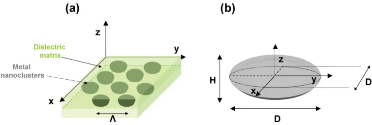
4.2.3 Influence of the morphological and organizational parameters of the metal nanoclusters . . . 46
4.3 From effective complex refractive index (nxy + ikxy) to the SDRS signal . 49 4.3.1 Comparison between nxy + ikxy and transmittance T or re-flectance R of the nanocomposite materials . . . . 49
4.3.2 Comparison between reflectance R and the relative reflectance (ΔR/R0) . . . 49
4.4 Limitations of the optical simulations . . . 52
4.4.1 Restriction to the diluted medium . . . 52
4.4.2 Limitation due to the image dipole approximation . . . 53
4.4.3 Restriction to spheroidal and identical nanoclusters . . . 53
5 Summary and conclusions . . . 54
Bibliography 57 III Monitoring the optical properties of materials during their deposition 65 1 Introduction . . . 65
2 Deposition of dielectric material (Si3N4) . . . 65
2.1 Experimental details . . . 66
2.2 In situ and real-time SDRS observations . . . . 67
3 Depositions of noble metals (Ag, Au, and Cu) . . . 68
3.1 Experimental procedure and real-time SDRS observations . . . 69
3.1.1 3D growth of metal nanoclusters . . . 70
3.1.2 Percolation regime in noble metals . . . 73
3.1.3 2D growth of noble metals . . . 75
4 Depositions of Si3N4:Ag:Si3N4 and Si3N4:Au:Si3N4 nano-composites . . . 75
4.1 Experimental procedure during the nanocomposite depositions . . . 75
4.2 Post mortem analysis of the nanocomposites . . . . 76
4.3 In situ and real-time SDRS observations . . . . 79
4.3.1 STEP 1: Deposition of Ag or Au on the Si3N4 buffer-layer (t ≤ 20/33sec) . . . 79
4.3.2 STEP 2: Holding time after the metal depositions (20/33sec ≤ t ≤ 620/633sec) . . . . 81
4.3.3 STEP 3: Pre-sputtering of the Si3N4 target (620/633sec≤ t ≤ 1670/1683sec) . . . 81
4.3.4 STEP 4: Deposition of the Si3N4 capping (1670/1683sec≤ t ≤ 2870/2883sec) . . . 82
5 Effect of the metal amount on the optical properties of Si3N4:Ag:Si3N4 nanocom-posites . . . 83
5.1 Experimental procedure . . . 83
5.2 Post mortem nanostructure analysis . . . . 84
5.3.1 STEP 1: Ag depositions on Si3N4 buffer-layers with increasing
Ag amounts . . . 86
5.3.2 STEP 2: Holding time after Ag depositions . . . 87
5.3.3 STEP 3: Pre-sputtering of the Si3N4 target (effect of N2 ions) . 88 5.3.4 STEP 4: Deposition of the Si3N4 capping layer . . . 89
5.3.5 Comparison of experimental and simulated SDRS signals . . . . 90
6 Summary and conclusions . . . 91
Bibliography 93 IV Monitoring the reactivity of Ag nanoclusters for different atmospheres 97 1 Introduction . . . 97
2 State of the art . . . 97
3 Reactivity of the metal nanoclusters for non-ionized gas atmospheres . . . 101
3.1 Experimental details . . . 101
3.2 Reactivity of Ag clusters under O2 atmosphere . . . 101
3.2.1 Post mortem nanostructure analysis . . . . 103
3.2.2 In situ and real-time SDRS analysis . . . . 104
3.2.3 Effect of Ag amount on the reactivity of the nanoclusters . . . . 108
3.3 Influence of different parameters on the reactivity of Ag nanoclusters with non-ionized gas . . . 109
3.3.1 Effect of O2 partial pressure . . . 110
3.3.2 Effect of substrate . . . 110
3.3.3 Effect of deposition temperature . . . 114
3.3.4 (Non)-reactivity of Ag clusters under N2 and Ar atmospheres . 117 4 Effect of partially ionized gases on the reactivity of Ag nanoclusters . . . 118
4.1 Experimental details . . . 118
4.2 Effect of partially ionized O2 on the Ag nanoclusters . . . 118
4.2.1 Post mortem nanostructure analysis . . . . 119
4.2.2 In situ and real-time SDRS analysis . . . . 122
4.2.3 Effect of partially ionized N2 . . . 124
5 Summary and conclusions . . . 126
V Monitoring the nanostructural and optical changes in Ag nanoclusters during
annealing treatments 131
1 Introduction . . . 131
2 Effect of thermal annealing on the Ag nanoclusters . . . 131
2.1 Experimental details . . . 132
2.2 Post mortem nanostructure analysis . . . . 133
2.3 In situ and real-time SDRS analysis . . . . 134
3 Effect of low energy bias plasma treatments . . . 137
3.1 Plasma annealing of non-oxidized Ag nanoclusters . . . 138
3.1.1 Experimental details . . . 138
3.1.2 Post mortem nanostructure analysis . . . . 139
3.1.3 In situ and real-time optical analysis . . . . 142
3.2 Bias plasma annealing of oxidized Ag nanoclusters . . . 146
3.2.1 Experimental details . . . 146
3.2.2 In situ and real-time optical analysis . . . . 146
4 Summary and conclusions . . . 149
Bibliography 151 General conclusion and perspectives 155 Appendix 159 1 Introduction . . . 159
2 Optical simulations . . . 159
2.1 Reflectance calculations . . . 160
2.2 Yamaguchi model . . . 163
2.2.1 Macroscopic response of the nanocomposite system . . . 163
2.2.2 Microscopic response of the nanoclusters . . . 164
2.2.3 Relation between macroscopic and microscopic responses . . . . 165
2.2.4 Calculation of local electric field Eloc . . . 166
2.3 Calculation of effective dielectric function εef f,u . . . 170
2.4 Modified dielectric function of metal nanoclusters (εi) . . . 171
2.5 Influence of inter-dependent cluster parameters on the simulated optical response . . . 172
2.5.1 Influence of the morphological parameters (D and H/D) at same cluster organization (Λ = constant) . . . 172
2.5.2 Influence of cluster size and inter-cluster distance for same
clus-ter shape . . . 173
3 Determination of cluster parameters using post mortem structural characteriza-tion techniques . . . 174
3.1 HAADF-STEM analysis . . . 175
3.2 GISAXS analysis . . . 177
3.2.1 GISAXS theory . . . 177
3.2.2 Experimental method and quantitative analysis . . . 179
Nanomaterials are the building blocks of today’s nanoscience and nanotechnology. Due to the distinct features of the nanomaterials, their utilization in the application sectors have increased the device miniaturization beyond ones imagination. In this regard, as an example, Moore’s law1 is famous in the domain of semiconductor technologies. However, in nanoscience,
as the demand for smaller device sizes is increasing faster and faster, the industries as well as the academic sectors are now facing new challenges and urgent needs to understand the properties of the materials at the nanoscale.
It is well known that, as we move from “bulk” to “nanoscale” dimensions, the material properties change surprisingly. Optical properties of the materials are not an exception to this fact. Applications based on the optical properties of nanomaterials span domains such as, optical detectors, lasers, optical sensors, imaging technologies, screen displays, solar cells, photocatalysis, biomedicine, etc. Especially, in case of noble metal nanoclusters, the optical response is dominated by the phenomenon of surface-plasmon resonance (SPR), classically described as the collective oscillation of the conduction electrons subjected to an electromagnetic excitation, which induces both, a wavelength-selective photon absorption in the visible range and a strong enhancement of the local electromagnetic field around the nanoclusters. As the optical response of the metal nanoclusters strongly depends upon their type, nanostructure (morphology and organization), and surrounding atmosphere, the understanding and control of these parameters are important. In addition, as these metal nanoclusters show remarkable sensitivity for the surrounding atmosphere comparing to their bulk counterparts, they are the current favorites for the nano-sensing applications. Besides, upon covering these metal
1Moore’s law predicts that the number of transistors per unit area on the integrated circuits will be doubled
nanoclusters in a protective dielectric matrix, a metal:dielectric nanocomposite structure is formed which has valuable applications in fields of opto-electronics, photonics, plasmonics, and photovoltaics.
In this context, the group called “Nanoparticules et Nanostructures” from “Départe-ment de Physique et Mécaniques des Matériaux” of “Institut Pprime” has dedicated its work to understand and control the growth and the optical properties of metal nanoclusters (Ag, Au, and Cu) covered by various dielectric matrices (BN, Si3N4, Al2O3, Y2O3). Extensive studies
have been made by this group in the past, which focused on the influence of the nanostruc-ture of the metal nanoclusters on their optical properties2,3,4, and on the influence of dielectric capping layers in modifying the morphology of the metal clusters, thus altering their optical response accordingly5,6,7. In addition to this, significant works have also been done on the
understanding of the optical response of self-organized metal nanoclusters, either in dielectric matrices, forming metal:dielectic multi-layer nanostructure systems8 or on faceted/rippled
di-electric surfaces giving rise to well-aligned nanocluster chains9,10. For the synthesis purposes,
ion-beam sputtering technique was implemented in all above research works, while the optical characterizations of the nanocomposite thin films were carried out by ex situ spectroscopic measurements in transmission or in reflection mode. In order to correlate the nanostructure of the metal clusters with their optical properties, post mortem structural characterization tech-niques were used like, high-angle annular dark-field scanning transmission electron microscopy (HAADF-STEM) and grazing-incidence small-angle X-ray scattering (GISAXS).
Compared to previous studies, the work reported in this thesis explores two new ap-proaches to study the properties of nanocomposite thin films. First, the nanocomposite thin films are grown by magnetron sputtering deposition. Second, a home-made in situ and real-time surface differential reflectance spectroscopy (SDRS) set-up is mounted on the magnetron sputtering chamber for their optical characterizations.
In the literature, dedicated use of SDRS can be seen for studying the optical properties of metal nanoclusters, but mainly during their growth by thermal evaporation11. Such
real-2S. Camelioet al. Applied Physics B: Lasers and Optics 80, 89-96 (2005).
3S. Camelioet al. Journal of Non-Crystalline Solids 352, 2501-2505 (2006).
4J. Toudertet al. Journal of Physics D: Applied Physics 40, 4614-4620 (2007).
5J. Toudertet al. Journal of Applied Physics 98, 1-10 (2005).
6D. Lantiatet al. Journal of Applied Physics 102, 113518 (2007).
7D. Babonneau et al. EPJ Applied Physics 44, 3-9 (2008).
8D. Lantiatet al. Review Advance Materials Science 15, 150-157 (2007).
9D. Babonneau et al. Physical Review B 80, 155434 (2009).
10D. Babonneau et al. EPL 93, 26005 (2011).
time optical diagnostics are extremely important because they not only offer valuable insights during the initial phases of a thin film growth, but also make possible the capture of the “missing-links” during the entire deposition processes that may not be always capable with
post mortem techniques. Especially, such conditions may arise during the alternate depositions
of two materials, or during different physical and chemical treatments of the deposited materials. This thesis explores such cases sequentially where the optical properties of metal nanoclus-ters are investigated with in situ SDRS in real-time during their deposition on different surfaces, during several physical and/or chemical treatments, and during their capping by a dielectric matrix (Si3N4) which not only protects them from the contaminations and aging processes, but
also improves their optical properties and “freezes” the modifications in the nanostructure. In order to study the morphology and organization of the nanoclusters, post mortem HAADF-STEM and GISAXS are implemented throughout this thesis. The details of the analysis are given in the respective chapters, which are organized in the following order,
- In Chapter I, as the properties of the deposited materials sensitively depends on their fabrication process, the advantages of magnetron sputtering deposition used during this work are comparatively discussed with other physical vapor deposition techniques. In this regard, the basic characteristic specifications and the multi-functional operations of our magnetron sputtering machine are presented. Further, different growth modes through which a metal evolves on a dielectric substrate are described in short considering thermodynamic and kinetic aspects.
- In situ and real-time SDRS used for the optical study of the nanocomposites during their depositions is first comparatively discussed with other sensitive optical characterization techniques in Chapter II. Then, in order to understand the influence of different param-eters on the optical properties of the nanocomposites, the Yamaguchi effective medium model12 is presented briefly. Moreover, the important limitations of optical models in
order to obtain the quantitative information are also discussed.
The results achieved during this research work are collected in Chapters III, IV, and V.
- In Chapter III, the use of in situ and real-time SDRS in studying the optical proper-ties of a dielectric material (Si3N4), metals (Ag, Au, and Cu), and their nanocomposites
is presented. After studying Si3N4 and noble metal depositions individually, real-time
variations in the optical properties of Si3N4:metal:Si3N4 nanocomposites, grown by
al-ternate depositions, are studied. Here, the insightful information given by the SDRS
are discussed thoroughly, as each deposition step modifies the optical properties of the metal nanoclusters accordingly. Furthermore in this chapter, the influence of the metal amount on the structural and optical properties of Si3N4:metal:Si3N4 nanocomposites is
also investigated.
- As Ag nanoclusters show strong reactive properties under gas exposure, Chapter IV mainly depicts their reactive interactions with different gases (O2, N2, and Ar), which
can be introduced in the magnetron chamber either in non-ionized or partially ionized form. As these reactive interactions change the optical properties of Ag nanoclusters, an extensive work is carried out to understand the effects of metal amount, gas flux and type, substrate type, and deposition temperature, on the optical properties of the Ag clusters in real-time. These “gas-reacted” Ag nanoclusters are then subsequently covered by a Si3N4 capping matrix and the modifications in the optical properties are registered and
discussed along with their structural modifications.
- Finally, the influence of annealing treatments on Ag nanoclusters is presented in Chapter V. Here Ag nanoclusters, after their growth on a substrate, are subjected to controlled annealing treatments (either by thermal annealing or by creating a low energy bias plasma around them), and then subsequently capped by a Si3N4capping matrix. As the annealing
treatment produces significant modifications in the nanostructure of the Ag clusters, it accordingly alters their optical properties, which can be sensitively captured with the help of in situ SDRS.
The important results obtained during this research work are specifically summarized in the general conclusion part, where possible future perspectives are also presented. At the end of this thesis, an appendix part holds extended details of the theoretical concepts related with the reflectance calculations and the Yamaguchi model. In addition to this, the details of image analysis procedures, with which the extraction of the nanostructure information from HAADF-STEM micrographs and GISAXS patterns is possible, are also enclosed.
Nanocomposite thin films: fabrication methods
and growth mechanisms
1
Introduction
In the world of materials science, thin films have created path breaking technological ad-vances. These thin films are thin layers of specific materials, which can range from mono-atomic to several micrometers in thickness and can have strikingly different properties than that of their bulk counterparts. Even though Bunsen and Grove first obtained thin films of metals in 1852, their extensive fabrication started in early 1960’s when the semiconductor materials found important applications in many electronic devices. Interesting applications of thin films were soon discovered in other areas like solar cells (Si), conductive thin films (ZnO), sensitive high temperature sensors (SiC), high temperature and high mechanical strength nitride thin films (TiN), thin film capacitors (SiO, Ta2O5, MnO2), high temperature superconductor thin
films (YBa2Cu3O7) etc [1–3].
More specifically, as the optical thin films can guide or modify the light characteristics precisely, it makes them ideal candidates for numerous applications, in opto-electronics, optical sensors, optical multilayer coatings, optical filters etc, e.g. metal thin films (such as, Au, Ag, Cu, Al, Cr etc) and metal-dielectric materials (also known as cermets, like GeSiTe-SiO2,
ZnS-SiO2, Ag-Si3N4 etc) have found important applications in plasmonics and photonics in the form
of optical data storage [4–6], optical nano antennas [7,8], optical waveguides [9], and nanoscale nonlinear optical devices like fast response optical switches [10–12]. In such applications it can be seen that the dielectric materials not only protect the nanoscale metals from aging processes and contaminations, but also improve their respective properties and functioning [13]. Other promising application areas for optical thin films can be in chemical and biochemical sensors, which use nano-scale materials like Au, Ag, with different dielectric substrates such as, Teflon,
TiO2, SiO2, ZnO, polymers to influence their sensing properties [14–19]. On the other hand,
research interest in nanomaterials like Au, Ag, Sb, Cu, ZnO, ZnS, dye synthesized TiO2, which
constitute basic materials for low cost and efficient solar cells over the traditional silicon-based solar cells, is on high demand [20–25].
As thin films give rise to promising applications, their fabrication techniques are important to address thoroughly. Hence, this part of the thesis is especially dedicated to nanocomposite thin film fabrication techniques. Here, different physical deposition methods are explained with more focus given particularly on the magnetron sputtering deposition technique as it is used in our case to deposit nanocermet thin films consisting of noble metals (Ag, Au, and Cu) and dielectric material (Si3N4). In addition to this, different mechanisms through which a thin
film grows on a substrate are also discussed in this chapter. On this basis, a detail account is given for the 3D growth of metal nanoclusters on dielectric substrates grown by physical vapor deposition.
2
Thin film deposition techniques
2.1
General schematics of deposition techniques
The act of forming thin layers of any material on a desired surface is known as thin film deposition. The qualities, properties, characteristics of the thin films sensitively depend on the deposition procedure and the technique used during their fabrications. During the deposition process, the materials to be deposited in the form of thin films are called as “target materials” and the surfaces on which the condensation or the deposition of the materials takes place are called as “substrates”. Any thin film deposition process involves three basic steps,
- the production of appropriate atomic species of the target material; - their proper transport on the substrate;
- their condensation on the substrate surface to form a solid deposit. A general schematics for the deposition techniques is given in Fig.I.1 below,
Based on the nature of the deposition processes, the thin film deposition techniques can be divided broadly into two categories, namely, physical vapor deposition (PVD) and chemical vapor deposition (CVD).
In PVD techniques, vapors of the desired materials can be generated, either by heating them thermally or by bombarding them with high energy electrons and/or ions in appropriate
Figure I.1 – Schematics of different thin film deposition techniques.
vacuum conditions. In such deposition methods, vacuum plays an important role in deciding the properties and quality of the thin film, hence the PVD techniques are often called as vacuum deposition techniques [26].
In contrast to this, CVD is a process where a solid material is deposited on the desired surface from its vapor phase during or after chemical reactions. It generally follows the sequence,
Gaseous reactants → Stable solid material (↓) + gaseous products (↑) [1, 3]
Here, the CVD relies on the reactive carrier gases that either decompose or react with other gases to produce stable reaction products of the desired materials (↓) on the substrate surface under controlled conditions, while gaseous products are given out of the system (↑). Both PVD and CVD are characteristic deposition methods for a wide range of materials that can be used in numerous applications. Hence, these two techniques are the backbone of the thin film deposition technology. As in our case the depositions were carried out using a physical way, we will stress only on the PVD techniques in detail.
2.2
Vacuum evaporation technique
Vacuum evaporation is one of the simplest and versatile deposition technologies used in thin film fabrications. The first attempt to create thin films with this method was done by Faraday in 1857 for metals and from then on, this technique has been involved in many thin film manufacturing industries [1]. It consists in the vaporization of the materials by heating them to a particular temperature, where the vapor pressure becomes appreciable and atoms or
molecules are lost from the target surface to condense on the substrate surface (e.g. Knudsen tube). This evaporation may be from a liquid surface (i.e. above the melting point) or from a solid surface (i.e. sublimation) [26]. In this deposition method, the vapors are produced from the source material which is heated by direct resistance, radiation or arc discharge. The heating can also be carried out with the help of high energy electrons, which will bombard the surface of the target material that results in the evaporation. During the evaporation, the whole system is kept in a deposition chamber in which necessary vacuum (around 10−7 to 10−10 mbar) is created. This vacuum plays an important role during the deposition process that allows the evaporated atoms to travel as freely as possible. It is also worth noting that vacuum evaporation is a low-energy process since the deposited material condenses on the substrate surface with a very small kinetic energy around 0.1-0.5eV [1, 3,27].
2.3
Sputter deposition techniques
Sputtering was originally developed to deposit refractory materials, which were not possible with the vacuum evaporation technique in the early days, but today this technique is a versatile thin film deposition technique for numerous materials that are used for research and industrial purposes [3]. It is a PVD process in which sufficiently energetic ions are used to bombard the surface of the target material. These ions are operated with controlled voltage and appropriate pressure is maintained in the deposition chamber. Due to this ion bombardment, the material atoms “pop out” from the material surface (also known as “sputtered” atoms), and are deposited on the substrate surface in the form of thin films [1,3]. Sputtering is a non-thermal vaporization process where the surface atoms of the target material are physically ejected by the momentum transfer from the energetic bombarding ions. Hence this method is known as an energetic deposition technique [26,28]. Sputter-ejected species can have kinetic energies around 5-100eV, which is much more than the thermal energy [1, 3, 27, 29].
In addition, it should be noted that, ion plating deposition also exists as a combination of both, vacuum evaporation and sputtering techniques in which the materials to be deposited are first vaporized by evaporation or sputtering and then bombarded by the atoms or ions of reactive gases. Like other techniques, it is also used for the dense coatings, hard coatings of compound materials on tools, high density optical coatings and coatings on complex surfaces etc . . . [26, 30, 31].
2.3.1 Ion beam deposition technique
Ion beam sputtering is generally used for the deposition of uniform thin films and for uniform etching purposes. In this technique, the ions of inert gas (generally plasma of Ar gas, Ar+) are
generated in a separate ion source chamber (ion gun), and the materials to be deposited on the substrate are directly bombarded by a continuous flux of these ions at low pressures of 10−4 mbar [2, 32]. The ions travel with very high energies (in the order of keV) towards the target materials and carry out sputtering processes. Due to the low pressures, the mean free path for the sputtered atoms is higher than in other sputtering deposition techniques explained below and hence, depending on the sputtering voltages, the energies of the sputtered atoms can be in the range of 5-200eV [1,27, 33].
There are many advantages with this technique, such as the low pressures in the deposition chamber which reduce the irradiations and contaminations in the deposited films. Also, as the substrate is not in contact with the plasma directly, substrate heating effects are reduced efficiently. Moreover, the generation of ions in a separate chamber allows the independency over the current densities and voltages, that extends its flexibilities over a wide range of materials [1, 2].
Even though this technique was less useful for practical depositions in early days due to the small beam size (around 1 cm) and low deposition rate, recent technical adaptations like ion thruster technology, helps to create larger beam sizes (around 10-30 cm) [3].
2.3.2 Cathode sputtering deposition technique
In the cathode sputtering technique, the target materials are subjected to appropriate high voltages upon which, they act as a cathode. Due to this voltage, the gas introduced at the vicinity of the target, converts into a plasma and spreads all over the target surface [3]. These energetic plasma ions collide with the atoms of the target materials with sufficient kinetic energies and the target atoms are ejected out due to such collisions [34]. The mean free path of these sputtered atoms is smaller than other deposition techniques because this technique operates around 10−2 mbar and hence, they are deposited with a kinetic energy in the range 5-10eV [29].
In the cathode sputtering technique, there are numerous parameters that have to be con-trolled precisely for the quality of the deposited thin film. Out of which, vacuum in the de-position chamber and sputtering voltage are the most important parameters along with the “sputtering process” which are described below,
• Vacuum - In cathode sputtering, before starting the sputtering process, sufficient
vac-uum (around 10−7 mbar) is created in the sputtering chamber to avoid the gaseous contaminations during the sputtering processes [26]. The mean free path of the sputtered atoms inversely depends on the pressure inside the chamber. If vacuum is not sufficient
and distance between the target and substrate is too large, the mean free path will reduce drastically and the sputtered atoms will not reach at the substrate surface with sufficient energies due to collisions with the gas atoms. The appropriate pressure, the distance be-tween the target-substrate and the substrate temperature, all together decide the quality of the deposited thin film [29, 34, 35].
• Voltage - The voltage at the target can be applied in the form of direct current (DC)
voltage or radio frequency (RF) voltage. This voltage defines the power during the sput-tering. Generally, for the conductors (metallic targets), DC voltage is applied because the free electrons are removed easily and does not accumulate on the target. Voltage (or power) influences the properties and quality of the thin film: e.g. Chan et al [36] have shown the effect of DC voltage along with Ar gas pressure on the electrical properties of Cu thin films. In cathode sputtering, the required DC voltage can be in the range of kV. On the other hand, RF sputtering is typically useful in the case of high insulating target materials, such as ceramics or oxides. The alternating tension helps the target to be neutral and accumulation of charges on the target surface is avoided [1], which maintains the sputtering rate constant. Even though RF sputtering can produce high quality ho-mogeneous thin films [36], it has relatively slower deposition rates than DC sputtering [29].
• The “sputtering” process - After the appropriate pressure formation in the deposition
chamber, the target material is subjected to the high voltage and acts as a cathode. Just few moments before this process, a definite flux of sputtering gas is introduced very close to the target surface. Sputtering gases are generally inert to avoid the reactions at target and substrate ends. The sputtering yield can be greater when the mass of the bombarding ions is similar or larger than that of the target atoms [1]. Hence, generally, Ar is the best choice for the sputtering gas but other gases like O2, N2 or their mixtures can be used for
reactive depositions [37].
Due to the high voltage, the Ar gas converts into a glow discharge plasma. Then the Ar+
ions get attracted towards the target rapidly and collide on the target atoms [38, 39]. Due to the sufficient momentum transfer from the Ar+ ions, the target atoms knock out from the target surface towards the substrate i.e the target is bombarded by Ar+ ions.
During the sputtering, secondary electrons get formed due to the ion bombardment and they play an important role in maintaining the plasma [29,38]. These target atoms leave the target surface with sufficient energy and get condensed on the substrate [29, 34].
Though this traditional deposition process of cathode sputtering was successful in the beginning, there were lots of limitations. Control over the secondary electrons to maintain the plasma state of the gas during sputtering and low ionization efficiencies in the plasma were the most important, which give rise to low deposition rates. In addition to this, thin film heating effects were also a prime concern due to the uncontrolled plasma formation that may result into modifications in the thin film properties [38]. These problems are reduced efficiently by the introduction of the magnetron sputtering technique where the plasma is well confined by the magnetic lines of forces within the chamber and nearer to the target material.
2.3.3 Magnetron sputtering deposition technique
Even though the first study of low pressure deposition with magnetic field was done by Penning in 1935, the true potential of the magnetron sputtering deposition technique in thin film fabrication was recognized from 1960s [1] Now, it is known as a powerful and flexible technique for the PVD coatings in commercial and scientific fields, and has a wide range of applications for the materials like metals, dielectrics, alloys, oxides, nitrides, composites and so on . . . [1, 3,39]
Though this technique was found to be superior in the thin film deposition, it took a long time to turn it into today’s sophisticated magnetron sputtering technique. The biggest problem was the control of the deposition process along with many parameters such as vacuum, voltage, gas flow, plasma control etc . . . [39]. But today the magnetron covers the limitations of the cathode sputtering technique and is appreciated for relatively high deposition rates, and low substrate heating effects [1]. In this technique, the controlled plasma of the sputtering gas ultimately controls the whole deposition process.
In magnetron sputtering systems, magnets are used at the base of target (FigI.2). These magnets create magnetic fields parallel to the target surface. The magnetic field lines are suf-ficiently strong to confine the “glow discharge” plasma at the target surface. The secondary electrons, which are formed due to the electron-ion bombardment, are affected by the combi-nation of electrostatic and magnetic forces and execute helical motion around these magnetic field lines [1,27,34,39]. Such trapped electrons advance in the field lines by collisions and they can have energies in the range of 100eV and hence, their collision with the sputtering gas atoms helps maintaining the plasma at the target surface. This increases the ionization efficiency of the gas resulting in a dense plasma surrounding the target region, which in turn increases the sputtering of the target [1]. This gives a higher sputtering rate at the target and hence a higher
deposition rate at the substrate. The increased ionization efficiency also allows maintaining the discharge glow at high pressures of 10−2-10−3 mbar [29] and at lower voltages around 300-500V, compared to the traditional ion-beam sputtering and cathode sputtering, which require high voltages in the order of kV [38, 40].
Figure I.2 –A typical magnetron sputtering system [39]. (©Angstrom Science, 2009 )
2.3.4 PUMA
In this work we have used the magnetron sputtering deposition machine called PUMA (for “Pulvérisation Magnetron”) for the depositions of metal-dielectric nanocomposites (AC450 Al-liance ConceptTM). PUMA (Fig.I.3) is a multi-functional and automatic machine which is used
in a “balanced way” with all the magnets having similar pole strength, giving rise to balanced magnetic lines of force that controls the gas plasma. It is a triple-cathode magnetron sputter deposition system. Here, the sputtering or deposition experiments are carried out in a steel vacuum chamber, controlled by a peripheral computer. PUMA has possible application areas in research and development for co-depositions, multilayer depositions, reactive depositions etc . . . Sputtering depositions of different metals, nitrides, oxides, semiconductors can be carried out with controlled parameters [37,41, 42]. The special features of PUMA are:
• Vacuum - Cryogenic pump is used to create the ultimate vacuum in PUMA, which can
Figure I.3 – Schematics of PUMA. Only two of the three magnetrons are shown for convenience.
around 10−2 to 10−3 mbar is sufficient which is higher compared to ion beam sputtering (∼10−6 mbar, respectively) [37].
• Target Materials - Three target magnetrons (out of which, only two are shown in
Fig.I.3 for convenience,) are mounted inside the deposition chamber with a symmetrical arrangement at 120◦ and inclined at 25◦from the substrate normal. The magnetrons used in PUMA are 3” GencoaTM Vtech target source. Each target is covered by a metal flap (shutter), which is fixed at one end and can semi-rotate in a perpendicular plane over the target. This shutter is helpful during the pre-sputtering of the target material, which prevents the material to be deposited on the substrate and other targets.
During sputtering, this shutter can slide away from the target automatically and the material deposition on the substrate starts as soon as the appropriate voltage is applied, converting the target material into a cathode. These targets are operated at a voltage range of 300-500V. Generally, RF voltage is used for dielectric materials, while metal targets are sputtered with DC voltage. The maximum power of the supply in RF mode
is 1.2kW, while in DC mode, it is 1.5kW. In PUMA, an appropriate voltage value, a controlled plasma gas, and a correct magnetic field around the target give rise to the desired deposition rate. The currently available targets in our laboratory are Ag, Al, Au, C, Cu, Mo, Ni, Si, Ti, W, Zr, TiAl, NiTi, Y2O3, SrTiO3, and Si3N4.
• Gas introduction - In PUMA, the gases that can be introduced other than Ar are
O2 and N2. It is possible to introduce the dosage of the single gas flux or gas mixtures
with precise control from 0.3 to 20 sccm (standard cubic centimeters per minute) on the target (through a gas inlet) or in the vacuum chamber (through a gas ring). In situ and real-time measurements of partial pressures are also possible for all these gases. For that purpose a Vision 1000P-MKSTM quadruple mass spectrometer is used. The range of this
mass-spectrometer is 1-200 amu (atomic mass unit) and the detector is made up of dual faraday/secondary electron multilayer. It monitors the process or analyzes the residual gases. More information regarding the gas introductions and the real-time measurements of the gas partial pressures is given in Chapter IV.
• Substrates - The substrates are kept at opposite side of the target in an horizontal plane.
Generally, depending upon the study, different substrates like glass or Si can be used. These substrates are fixed on a substrate holder along with the carbon coated copper grids if Scanning Transmission Electron Microscopy (STEM) analysis is required. The substrate holder can be fixed or subjected to precise controlled rotations (which is not used in our case) and also, the distance between the substrate and target can be changed. In addition to this, the temperature of the substrate can be changed by controlled heating with the help of infra-red radiations heater and can be measured accurately using a chromel-alumel thermo-couple. An additional discussion regarding the heating arrangement in PUMA can be seen in Chapter V (Section 2)
• Plasma - In our case, we use a plasma of Ar gas to sputter the target materials. This Ar
gas can be introduced very close to the target surface as well as in the vacuum chamber with a precise flux automatically whenever needed. Here, to confine the Ar plasma during sputtering, balanced magnets are used to create the magnetic field lines of strength not greater than 250 Gauss so that only electrons are better confined to maintain the plasma than the gas ions [27]. Also, in PUMA, it is possible to create a controlled RF plasma of gas at the substrate end (due to the biased voltage maintained at the substrate, hence also known as bias plasma). This feature of PUMA gives an interesting advantage as the plasma in such a configuration is in the vicinity of the substrate (and hence, very close to
the deposited thin film). In this regard, more information on the bias plasma formation can be seen in Chapter V (Section 3).
3
Mechanisms in thin film growth
3.1
A thermodynamic aspect
The growth of a thin film deposited on a substrate prominently depends upon the interac-tions between the atoms of the deposited material and of the surface of the substrate [43, 44]. The total free energy of the system can be given as,
Ef ree = γM − γS + γI, (I.1)
where, γM is the surface energy of the deposited material on the substrate, γS is the surface
energy of the substrate, and γI is the free energy of the interface between the thin film and the
substrate, which is generally small compared to γM and γS [45]. Based on this thermodynamic
relation, the growth of thin films can be modeled into three major mechanisms.
3.1.1 Three-dimensional (3D) or Volmer-Weber (VW) growth
In the VW type growth, 3D growth of the material can be seen on the solid surfaces. (γM + γI) greater than the surface energy of the substrate γS, i.e.
Ef ree > 0. (I.2)
Hence, the deposited material has tendency to form 3D clusters on the substrate surface and with the increase in the deposition time, the clusters grow in size (Fig.I.4). In other words, the low affinity of the deposited material towards the substrate leads to a 3D growth [45]. Such a 3D growth mode is seen in case of many metals deposited on insulators, on alkali halides and graphite [44,45]. Moreover, Campbell [45] has given details on the surface energies for different metals deposited on oxide surfaces.
3.1.2 Two-dimensional (2D) or Frank-Van Der Merwe (FM) growth
In the FM type growth, the materials have totally opposite properties than in the VW growth, i.e.
Figure I.4 – A 3D island or VW growth of the material on the substrate surface.
Hence, the atoms deposited on the surface will form a continuous layer. Then, this primary layer of atoms will be covered by the following atoms, and a layer by layer structure will be formed (Fig.I.5).
Figure I.5 – A 2D layer by layer or FM growth of the material on the substrate surface.
Such a FM growth mode is generally observed in the deposition of rare gases on graphite or on metals, also in metal-metal systems, and in the growth of semiconductor materials on semiconductor surfaces [43, 44].
3.1.3 Mixed (2D+3D) or Stranki-Krastanov (SK) growth
The SK growth mode is a mixed mechanism of FM and VW type growth. In case of ideal SK growth, a layer by layer growth of a material on a substrate is followed by the 3D growth of clusters or aggregates of the same material (Fig.I.6). Here the role played by the interface energy between the atoms and the substrate is not well known [40,44].
However, it is worth noting that a Pseudo SK growth can also be seen, where the deposition of the material on the substrate favors a 3D growth up to a critical stage and then, the
addi-Figure I.6 – An ideal SK growth of the material on the substrate surface.
tionally deposited material grows into an almost layer by layer or FM type growth on the top of these 3D clusters. The uncovered remaining fraction of the substrate surface between these clusters is then filled rather slowly by the additionally deposited material during the deposition [43, 44, 46].
3.2
Movements of atoms on the substrate surface - A surface
kinet-ics aspect
The surface kinetics aspects of the deposited atoms during the thin film deposition are important to understand because even if the system is thermodynamically favored, the kinetic limitations can deny the production of stable structures on the solid surfaces [43, 45].
During the deposition, the atoms of the deposited material condense on the substrate sur-face due to adsorption (i) with energy Ea. These isolated, individual adsorbed atoms on the surface are called adatoms, which are mobile on the substrate under the influence of the surface energies. This adsorption and mobility of the adatoms depend upon the respective materials, deposition rate and the temperature of the substrate. These adatoms, undergo different diffu-sion processes (ii) all over the surface until they are lost or trapped by several processes [44] such as,
- re-evaporation (iii) that takes place if the adatoms get sufficient energy to overcome the bonding between atom and substrate;
- trapping in surface defects (a) as the real surfaces can have many imperfections like, vacancies, dislocations, impurities etc, which can give a favorable site for the adatoms;
Figure I.7 – Different surface kinetics of atoms during thin film growth.
- trapping in a small group of adatoms called cluster (made up of few atoms) or they end up by forming a pair with an other isolated adatom and become a dimmer (b);
These diffusion processes contribute in the nucleation and growth of nanoclusters. During the diffusion, kinetics in the adatoms lead them towards the aggregation process (iv), where, the individual adatoms can join already existed 2D or 3D clusters depending upon the materials, substrates and free energy considerations [40,46]. Although cluster formation is normal in this process, there will be a critical size of clusters above which the probability of the
cluster growth in size will be greater than the probability of their decay. Hence, growth of a cluster is a nucleation phenomenon and the clusters above a critical size are referred as stable clusters which can grow in size during deposition process but difficult to decay [43, 44]. In contrast to the aggregation process where clusters tend to grow into bigger clusters, the process of dissociation (v) can be seen, where the detachment of the atom(s) from the clusters to substrate surface can take place. In this process, unstable adatoms from a cluster can dissociate and again diffuse on the substrate or vice versa.
The dissociation can be important if the deposited materials and substrate have same bond-ing energy, e.g. semiconductor on semiconductor, metal on metal etc... but, desorption of the majority of metal atoms on the oxide materials is negligible if the temperature of the oxide substrate is not near the evaporation temperature of the metal [46].
3.3
Different growth regimes in a metal thin film during their
de-position on a dielectric surface
In our case, we are interested in the 3D growth of metals on dielectric substrates, so, it will be interesting to understand the different stages involved in such a process from the beginning of the metal deposition to the formation of a continuous film [47]. We can explain these stages and their features as above.
3.3.1 Nucleation processes to form clusters
This is the first basic step that can be seen during the deposition. Here, the metal atoms with sufficient energy arrive on the dielectric surface, which is maintained at a particular temper-ature. This growth stage is characterized by the increasing density of the adatoms and their nucleation into 3D clusters on the dielectric surface. This growth step may take place due to two reasons,
• Nucleation due to the aggregation of the adatoms - This homogeneous type
of nucleation takes place entirely due to the contribution of the adatoms. Here, the nucleating adatoms combine with each other and with other 3D clusters on the substrate surface. Two adatoms may come in influence by accident or by the process of surface diffusion. This aggregation of the adatoms leads them to form stable structures on the oxide surface in the form of 3D clusters. This phase of the thin film growth is sensitive and depends upon the diffusion coefficient of the adatoms, their surface energies, temperature of the substrate, and the deposition rate [48].
• Nucleation due to the defects on the substrate surface - This is an heterogeneous
type of nucleation, where the defects/imperfections on the surface act as pining points for the adatoms and give rise to nucleation sites on the surface.
3.3.2 Growth of the clusters
During the regime of nucleation, there is always incorporation of new arriving atoms on the surface. Due to this tendency, the metal clusters tend to grow in the size. This growth can be due to the adsorption of the newly added adatoms on the already present stable clusters (growth due to direct condensation or out-of-plane growth) or it may be due to the diffusion among the clusters (in-plane surface diffusion). This atomic mass transport is possible via 2D or 3D cluster diffusion. Such Brownian motions of clusters take place due to various atomic transports across
the substrates as explained in some works in detail [49]. In case of 2D clusters, the growth is governed by the peripheral diffusion, condensation and movement of surface defects e.g. the diffusion of 2D clusters is possible by gliding on the surface as whole cluster [49, 50]. In case of 3D clusters, the rotational and translational movements of the clusters is seen contributing in the growth. Also, diffusion coefficient and temperature take a major role during the growth of 3D clusters [51].
3.3.3 The regime of coalescence
Due to the growth of the clusters, the cluster size increases continuously with the deposition time. After sufficient growth, the clusters coming into the vicinity with each other give rise to the coalescence regime. If two clusters come in contact under favorable thermodynamic conditions then they merge to form a single bigger cluster. During this regime, an increase in the cluster size is accompanied by a decrease in the cluster surface-density [52, 53]. Also, dynamic coalescence can be seen if the high mobility of small clusters contributes to the growth of the bigger clusters [52,54].
3.3.4 The regime of percolation
With the continuous deposition, further growth of the clusters can be seen. The clusters go on increasing and eventually reach a stage where they start to agglomerate. It is a regime where the coalescence is no more efficient in the particles due to their bigger sizes. Hence, the lateral growth rate of the clusters decreases rapidly. At this stage, the whole cluster system can be treated as one big loosely connected cluster, and the cluster surface density eventually decreases towards zero. This stage in the thin film growth is called percolation and at this point, the properties of the thin film, such as, electrical and optical properties, can alter significantly [55]. Determination of this percolation threshold in the ultra-thin films is thus important and has several applications e.g in thin silver coatings, in charge conducting films etc . . . [55,56].
3.3.5 Continuous or thick layer formation
The last regime in the thin film growth is the formation of a continuous layer. With the continuous deposition of the material, the gap or separation between the percolation areas is filled directly and progressively due to incoming atoms [55]. Generally, the properties of the materials in this regime are similar to their bulk counterparts. The schematics of the cluster density variation with the increasing metal amount in the VW type growth, is given in Fig.I.8.
Figure I.8 – Schematics of the cluster density variation with the increasing deposition amount of the
metal, showing important regimes of the cluster growth during thin film formation [1,47].
In summary, during the early steps of deposition, nucleation and growth are prominent in which small clusters are formed rapidly and their number per unit area (areal surface density of the clusters) increases. It is then followed by the coalescence regime, which induces an increase of the cluster size and reduction in the areal cluster density. During the VW growth, this stage form bigger clusters which are distinctly separated from each other. The continuous deposition further imposes a state of percolation where the areal surface density eventually reduced to zero by forming a structure made up of loosely connected bigger clusters. Further deposition then leads to the formation of a continuous layer where the gaps from the percolation regime are eventually filled out by the direct incorporation of the incoming atoms.
4
Summary and conclusions
In this chapter, we have seen a brief overview of thin film fabrication techniques that have been developed over last few decades. Out of these techniques, sufficient stress is given on the magnetron sputtering deposition technique which is used in this research work to fabricate the metal:dielectric nanocomposite thin films. Since with magnetron system we can deposit the ma-terials with different features, such as, automatic deposition process at low pressures, controlled current-voltage configuration, precise introduction of gas flux, real-time partial-pressure mea-surements, and reliable confinement of gas plasma during deposition, the magnetron deposition technique gives us flexibility over performance during the experiments.
After the fabrication techniques, we have seen different growth mechanisms and surface kinetics through which a thin film can evolve on a substrate surface. As these mechanisms play a vital role in the properties and the qualities of the deposited thin films, their knowledge deserves sufficient account for discussion. Then specifically, the important regimes for metal thin films following the 3D Volmer-Weber growth mode (starting from the nucleation of adatoms to the formation of continuous layer), are explained which give an idea about the metal adatom-cluster behavior during the on-going deposition.
[1] R. F. Bunshah. Handbook of deposition technologies for films and coatings. Noyes Pub-lications (1994). 5, 7, 8, 9, 10, 11, 21
[2] K. Wasa and S. Hayakawa. Handbook of Sputter Deposition Technology - Principles,
Technology and Applications. Noyes Publications (1991). 5, 9
[3] A. Elshabini-Riad and F. D. Barlow-III. Thin Film Technology Handbook. McGraw-Hill (1997). 5,7, 8,9, 11
[4] S. Park and J. W. Hahn. Plasmonic data storage medium with metallic nano-aperture
array embedded in dielectric material. Optics Express 17, 20203–20210 (2009). 5
[5] M. Mansuripur, A. R. Zakharian, A. Lesuffleur, S. H. Oh, R. J. Jones, N. C. Lindquist, H. Im, A. Kobyakov, and J. V. Moloney. Plasmonic nano-structures
for optical data storage. Optics Express 17, 14001–14014 (2009). 5
[6] K. P. Chiu, K. F. Lai, and D. P. Tsai. Application of surface polariton coupling
between nano recording marks to optical data storage. Optics Express 16, 13885–13892
(2008). 5
[7] B. Lee, I. M. Lee, S. Kim, D. H. Oh, and L. Hesselink. Review on subwavelength
confinement of light with plasmonics. Journal of Modern Optics 57, 1479-1497 (2010) 57,
1479–1497 (2010). 5
[8] L. Novotny. Effective wavelength scaling for optical antennas. Physical Review Letters 98, 266802 (2007). 5
[9] J. Homola, S. S. Yee, and G. Gauglitz. Surface plasmon resonance sensors: review. Sensors and Actuators, B: Chemical 54, 3–15 (1999). 5
[10] S. A. Maier, M. L. Brongersma, P. G. Kik, S. Meltzer, A. A. G. Requicha, and H. A. Atwater. Plasmonics - a route to nanoscale optical devices. Advanced Materials 13, 1501–1505 (2001). 5
[11] M. Dragoman and D. Dragoman. Plasmonics: Applications to nanoscale terahertz
and optical devices. Progress in Quantum Electronics 32, 1–41 (2008). 5
[12] G. Ma, J. He, and S. H. Tang. Femtosecond nonlinear birefringence and nonlinear
dichroism in Au:Tio2 composite films. Physics Letters, Section A: General, Atomic and
Solid State Physics 306, 348–352 (2003). 5
[13] F. R. Flory. Thin Films for Optical System. Marcel Dekker, Inc, (1995). 5
[14] B. Brian, B. Sepulveda, Y. Alaverdyan, L. M. Lechuga, and M. Kall.
Sen-sitivity enhancement of nanoplasmonic sensors in low refractive index substrates. Optics
Express 17, 2015–2023 (2009). 6
[15] B. Liedberg, C. Nylander, and I. Lundstrom. Biosensing with surface plasmon
resonance - how it all started. Biosensors and Bioelectronics 10, i–ix (1995). 6
[16] D. J. Sirbuly, A. Too, M. Law, R. Fan, and P. Yang. Multifunctional nanowire
evanescent wave optical sensors. Advanced Materials 19, 61–66 (2007). 6
[17] H. Meixner and U. Lampe. Metal oxide sensors. Sensors and Actuators B: Chemical 33, 198–202 (1996). 6
[18] N. E. Stankova, I. G. Dimitrov, P. A. Atanasov, T. Sakano, Y. Yata, and M. Obara. Nanostructured optical waveguide films of TiO2 and WO3−x for photonic gas
sensors. Thin Solid Films 518, 4597–4602 (2010). 6
[19] O. A. Sadik, S. K. Mwilu, and A. Aluoch. Smart electrochemical biosensors:from
advanced materials to ultrasensitive devices. Electrochimica Acta 55, 4287–4295 (2010). 6
[20] R. Konenkamp, L. Dloczik, K. Ernst, and C. Olesch. Nano-structures for solar
cells with extremely thin absorbers. Physica E: Low-Dimensional Systems and
Nanostruc-tures 14, 219–223 (2002). 6
[21] W. E. Vargas and G. A. Niklasson. Optical properties of nano-structured
dye-sensitized solar cells. Solar Energy Materials and Solar Cells 69, 147–163 (2001). 6
[22] G. Rothenberger, P. Comte, and M. Gràtzel. Contribution to the optical design
of dye-sensitized nanocrystalline solar cells. Solar Energy Materials and Solar Cells 58,
321–336 (1999). 6
[23] A. B. Kashyout, M. Soliman, M. El Gamal, and M. Fathy. Preparation and
char-acterization of nano particles ZnO films for dye-sensitized solar cells. Materials Chemistry
and Physics 90, 230–233 (2005). 6
[24] G. Zhao, H. Kozuka, and T. Yoko. Sol-gel preparation and photoelectrochemical
properties of TiO2 films containing Au and Ag metal particles. Thin Solid Films 277,
[25] K. Zakrzewska, M. Radecka, A. Kruk, and W. Osuch. Noble metal/titanium
dioxide nanocermets for photoelectrochemical applications. Solid State Ionics 157, 349–356
(2003). 6
[26] D. M. Mattox. The Foundations of Vacuum Coating Technology. Noyes Publications (2003). 7, 8, 9
[27] R. Bunshah. Handbook of hard coatings: Deposition technologies, Properties and
Appli-cations. Noyes publications (2001). 8, 9, 11, 14
[28] G. K. Hubler and J. A. Sprague. Energetic particles in PVD technology:
particle-surface interaction processes and energy-particle relationships in thin film deposition.
Sur-face and Coatings Technology 81, 29–35 (1996). 8
[29] A. Billard and F. Perry. chapter Pulvérisation Cathodique Magnetron. 8,9, 10, 12
[30] D. M. Mattox. Handbook of Physical Vapor Deposition (PVD) processing. Noyes Pub-lications - USA (1998). 8
[31] M. L. Hitchman and K. F. Jensen. Chemical Vapor Deposition- Principles and
Ap-plication. Academic press limited (1993). 8
[32] H. R. Kaufman. Technology of ion beam sources used in sputtering. Journal of Vacuum Science and Technology 15, 272–276 (1978). 9
[33] P. Martin. Handbook of deposition technologies for films and coatings (Third Edition). Elsevier Inc. (2009). 9
[34] www.pvd-coating.co.uk. 9, 10, 11
[35] S. Negi, R. Bhandari, L. Rieth, and F. Solzbacher. Effect of sputtering pressure
on pulsed-DC sputtered iridium oxide films. Sensors and Actuators B: Chemical 137,
370–378 (2009). 10
[36] K.-Y. Chan, P.-Q. Luo, Z.-B. Zhou, T.-Y. Tou, and B.-S. Teo. Influence of
direct current plasma magnetron sputtering parameters on the material characteristics of polycrystalline copper films. Applied Surface Science 255, 5186–5190 (2009). 10
[37] L. Simonot, D. Babonneau, S. Camelio, D. Lantiat, P. Guérin, B. Lamongie, and V. Antad. In-situ optical spectroscopy during deposition of Ag:Si3N4 nanocomposite
films by magnetron sputtering. Thin Solid Films 518, 2637–2643 (2010). 10, 12,13
[38] P. J. Kelly and R. D. Arnell. Magnetron sputtering: a review of recent developments
and applications. Vacuum 56, 159–172 (2000). 10, 11, 12
[40] D. Lantiat-Baillargue. Morphologie et auto-organisation de nanoparticles d’argent
dispersées dans des matrices diélectriques: influence sue les propriétés optiques. Thèse de
Doctorat, PhyMat - Université de Poitiers, Poitiers (2008). 12, 16, 18
[41] G. Abadias and P. Guérin. In-situ stress evolution during magnetron sputtering of
transition metal nitride thin films. Applied Physics Letters 93(11), 111908 (2008). 12
[42] A. Fillon, G. Abadias, A. Michel, and C. Jaouen. Stress and microstructure
evolution during growth of magnetron-sputtered low-mobility metal films: Influence of the nucleation conditions. Thin Solid Films 519, 1655–1661 (2010). 12
[43] J. L. Robins. Thin film nucleation and growth kinetics. Applied Surface Science 33/34, 379–394 (1988). 15, 16, 17,18
[44] J. A. Venables, G. D. T. Spiller, and M. Hanbucken. Nucleation and growth of
thin films. Rep Prog Phys 47, 399–459 (1984). 15, 16,17, 18
[45] C. T. Campbell. Ultrathin metal films and particles on oxide surfaces: structural,
elec-tronic and chemisorptive properties. Surface science reports 27, 1–111 (1997). 15, 17
[46] J. Carrey. Croissance granulaire d’Or et de Cobalt sur alumine amorphe:
caracterisa-tions et Simulacaracterisa-tions de Monte-Carlo. Thèse de Doctorat, Orsay - Université de Paris XI,
Orsay (2001). 17,18
[47] J. E. Greene. Low-energy ion bombardment during film deposition from the vapor phase:
Effects on microstructure and microchemistry. Solid State Technology 30, 115–122 (1987).
19, 21
[48] G. Hass, A. Menck, H. Brune, J. V. Barth, J. A. Venebles, and K. Kern.
Nucleation and growth of supported clusters at defect sites: Pd/MgO(001). Physical Review
B 61 (16), 11105–11108 (2000). 19
[49] S. V. Khare, N. C. Bartelt, and T. L. Einstein. Diffusion of monolayer adatom
and vacancy clusters: Langevin Analysis and Monte-Carlo Simulations of their Brownian Motion. Physical Review Letters 75, 2148 (1995). 20
[50] S. C. Wang and G. Ehrlich. Diffusion of large surface clusters: direct observations
on Ir(111). Physical Review Letters 79, 4234 (1997). 20
[51] A. Masson, J. J. Metois, and R. Kern. Migration Brownienne de cristallites sur une
surface et relation avec lépitaxie. Surface Science 27, 463–482 (1971). 20
[52] C. Templier, S. Muzard, A. Galdikas, L. Pranevicius, J. Delafond, and J. C. Desoyer. A phenomenological study of the initial stages of film growth. Surface and Coatings Technology 125, 129–133 (2000). 20