Any correspondence concerning this service should be sent to the repository administrator:
[email protected]
O
pen
A
rchive
T
oulouse
A
rchive
O
uverte (
OATAO
)
OATAO is an open access repository that collects the work of Toulouse researchers
and makes it freely available over the web where possible.
This is an author -deposited version published in:
http://oatao.univ-toulouse.fr/
Eprints ID: 4718
To link to this article: DOI:10.1109/LED.2011.2125940
URL:
http://dx.doi.org/10.1109/LED.2011.2125940
To cite this version: GOIFFON Vincent, MAGNAN Pierre, MARTIN-GONTHIER
Philippe, VIRMONTOIS Cédric, GAILLARDIN Marc. Evidence of a novel source of
random telegraph signal in CMOS image sensor. IEEE Electron Device Letters, 2011, vol.
32, n°6, pp. 773-775.
Evidence of a Novel Source of Random Telegraph
Signal in CMOS Image Sensors
V. Goiffon, Member, IEEE, P. Magnan, Member, IEEE, P. Martin-Gonthier, Member, IEEE,
C. Virmontois, Student Member, IEEE, and M. Gaillardin, Member, IEEE
Abstract—This letter reports a new source of dark current
ran-dom telegraph signal in CMOS image sensors due to meta-stable Shockley–Read–Hall generation mechanism at oxide interfaces. The role of oxide defects is discriminated thanks to the use of ionizing radiations. A dedicated RTS detection technique and sev-eral test conditions (radiation dose, temperature, integration time, photodiode bias) reveal the particularities of this novel source of RTS.
Index Terms—Active pixel sensors (APS), CMOS image sensors
(CIS), dark current, interface states, random telegraph signal (RTS), shallow trench isolation (STI), total ionizing dose (TID).
I. INTRODUCTION
T
WO types of parasitic random telegraph signals (RTS) are known to degrade the performances of CMOS im-age sensors (CIS). The first is an enhancement of the sensor temporal readout noise due to the discrete fluctuation of the in-pixel source follower (SF) channel conductance [1] (explained by channel carrier trapping and emission by oxide traps). The second type of CIS RTS is a discrete variation of the photodiode dark current (DC-RTS). Two sources are known for this latter phenomenon. The first one has been identified in proton irra-diated charge coupled devices (CCD) in the mid-1990s [2], [3] and a few years later in CIS [4], [5]. This source of DC-RTS was clearly attributed to displacement damage induced meta-stable generation centers located in the depleted volume of CCDs and CISs. At this time, ionizing radiation sources, such as 60Co γ-rays, were used to see if oxide defects could play a role in this kind of DC-RTS. It was clearly shown [2]–[5] that ionizing radiation did not induce DC-RTS in CCDs and in LOCOS-based CISs, leading to the conclusion that DC-RTS in CISs was not due to oxide defects but to bulk damages only. A second rare source of DC-RTS (due to trap assisted tunneling in gate oxide) has been reported at least once [6] in CIS manufactured with a 0.15 µm CMOS process, not optimized for imaging application where high electric fields exist in the vicinity of the reset MOSFET gate.In this letter, we report a new source of DC-RTS due to meta-stable Shockley–Read–Hall (SRH) generation mechanism at depleted oxide interfaces. As it is demonstrated in the fol-lowing, this DC-RTS is very similar to displacement damage
V. Goiffon, P. Magnan, P. Martin-Gonthier, and C. Virmontois are with the Université de Toulouse, ISAE, 31055 Toulouse, France.
M. Gaillardin is with CEA, DAM, DIF, 91297 Arpajon, France.
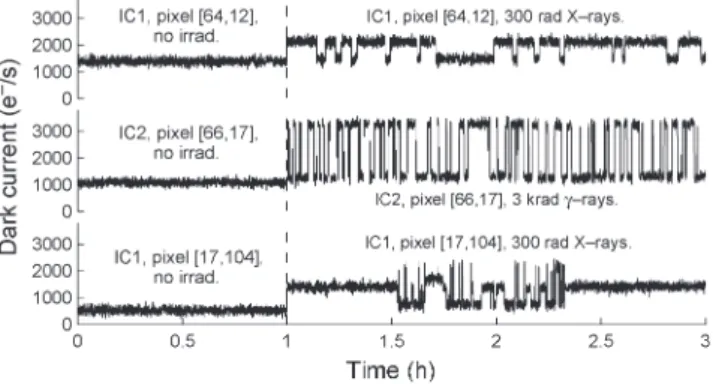
Fig. 1. Temporal representation of a selection of typical DC-RTS.
DC-RTS except that it is due to meta-stable oxide generation centers (most likely located at the shallow trench isolation (STI) interface) instead of meta-stable bulk generation centers. These meta-stable SRH generation centers are probably similar to those at the origin of DRAM variable retention time [7].
II. EXPERIMENTALDETAILS
The studied image sensors (IC1 and IC2) are 10µm-pitch 128 × 128-pixel arrays with 3T-pixels and manufactured using a 3.3 V commercial STI based 0.18µm CMOS image sensor process.
An automated RTS detection and RTS parameter extraction algorithm, initially developed to study displacement damage in-duced RTS, was used to detect dark current discrete transitions. This method, described in detail and validated in [8], relies on a typical edge detection technique in the temporal domain.
In order to discriminate the role of oxide defects and silicon bulk defects, ionizing radiation sources were used to gener-ate only oxide defects (interface stgener-ates and positive trapped charges). Two sources have been used: 10 keV X-rays for IC1 and 60
Co gamma rays for IC2. Radiation doses are given in rad(SiO2).
III. RESULTS ANDDISCUSSION
A selection of DC-RTS revealed after exposure to ionizing radiation is presented in Fig. 1. These signals represent the dark current of three selected pixels as a function of time. The observed RTS are very similar to what is generally observed in the case of bulk defect induced DC-RTS, except that the oxide RTS amplitudes appear smaller than bulk defect DC-RTS amplitudes. The dark current of pixel 17:104 shows that such
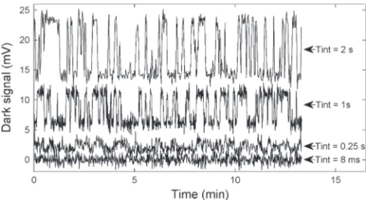
Fig. 2. Influence of the integration time on the studied RTS behavior clearly showing that the observed RTS are DC-RTS.
Fig. 3. Mapping of detected RTS pixels (white dots) for several TID: (a) IC1 before irradiation, (b) IC1 300 rad, (c) IC1 1 krad, (d) IC2 3 krad, (e) IC2 10 krad, (f) IC2 30 krad. Integration time = 1 s, sampling time = 2 s, measurement duration 12 h, temperature = 22◦C. The mean dark currentId
value after each irradiation is indicated under each figure.
RTS can be nonstationary, and that a single RTS defect can lead to more than two dark current discrete levels (as in the case of bulk defect RTS). The observed RTS is clearly not a source follower induced RTS temporal noise because the RTS amplitudes reported in this paper are directly proportional to the integration time (as illustrated in Fig. 2), whereas source follower induced RTS noise is known to be independent of integration time. Moreover, the RTS time constants reported here are more than two orders of magnitude longer than the slowest source follower RTS than can passes through the high-pass delta double sampling filter (intersample time about 2µs). The mappings of detected RTS before and after exposure to X andγ-rays are presented in Fig. 3. It can clearly be seen that RTS pixels are detected in unirradiated devices. This number of detected RTS pixels rises with total ionizing dose (TID) indicating that oxide defects are responsible.
Fig. 4 presents the distributions of the RTS maximum transi-tion amplitudes. The main part of the distributransi-tions appears to be exponentially distributed. Extracting the exponential slope of these distributions yields the exponential distribution average value 1/λ. These exponential distributions are shifted by the irradiation but they keep the same 1/λ. It strongly suggests that
Fig. 4. RTS maximum transition amplitude distribution for several TID (same test conditions as Fig. 3). The average value and the exponential 1/λ parameter of each distribution are respectively about 270 e−/s and 1/λ = 110 e−/s.
Extreme values go up to 2700 e−/s.
Fig. 5. Distribution of the mean time between two RTS transitions as a function of TID (same test conditions as Fig. 3).
the nature of the created defects does not change with TID, only their number increases. It confirms that the number of pixels exhibiting discrete switching behaviors, increases with TID, and therefore with the generation of oxide defects. It must be emphasized that the extracted value(1/λ = 110 e−/s)
is ten times smaller than the one extracted on displacement damage induced DC-RTS distributions (about 1200 e−/s [8]).
It is also important to notice that the RTS pixels observed before irradiation behave similarly to the ones detected after irradiation, with the same average amplitude. It strongly sug-gests that the DC-RTS observed in unirradiated devices are also due to this oxide defect induced DC-RTS. A slight change of exponential slope can be noticed after 30 krad. This is most likely due to the fact that several RTS defects are located in most pixels, leading to larger apparent maximum amplitudes at this TID. Finally, one can see that the weakest RTS fluctuations are not detected leading to a divergence, at low amplitudes, between the exponential fits and the measured distributions. This is due to the readout and shot noises which hide the low-amplitude RTS.
As regards the number of RTS levels per pixel, it was also observed to increase with TID (mainly two levels before irradiation and up to seven levels after 30 krad). This increase can be explained both by the superimposition of more than one RTS oxide defect contribution per pixel and by the creation of multi-level RTS oxide defects (e.g., pixel 17:104 in Fig. 1).
The distributions of the mean time between two transitions are illustrated in Fig. 5. The cutoff at short transition time is
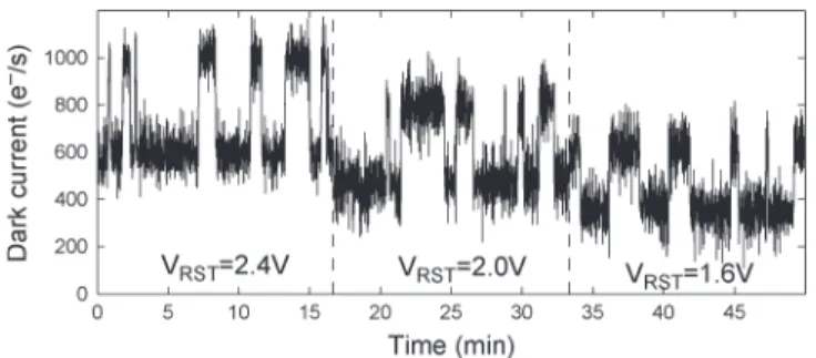
Fig. 6. Influence of the photodiode (hard) reset bias on the RTS amplitude. VDD= 3.3 V.
Fig. 7. Influence of the temperature on the RTS behavior. RTS amplitude Eact= 0.59 eV. Dark current pedestal Eact= 0.64 eV.
due to the lower limit of the detection process (which depends on the integration time and the number of detection filter coefficients [8]). It can be seen that the detected RTS time constant range covers entirely the detection window (i.e., from a few times the filter length to the measurement duration) and is expected to extend further if shorter sampling time or longer observation time are used. Hence, the physical process at the origin of this meta-stability does not appear restricted to a particular time range.
As regards the effect of electric field on the reported DC-RTS, Fig. 6 shows that the DC-RTS amplitude is very weakly dependent on the photodiode reverse bias, whereas the mean dark current is reduced with the depletion width reduction. Hence, it can be inferred that this kind of DC-RTS is not dom-inated by an electric field dependent contribution in contrary to what was observed in trap assisted tunneling DC-RTS [6]. This is confirmed by the DC-RTS activation energy around 0.6 eV (see Fig. 7 for example) and the mean dark current activation energy (Eact= 0.63 ± 0.03 eV on the whole array),
both around the midgap value, typical for SRH generation currents.
In CIS 3T-pixels, the photodiode depletion region is in contact with the STI interface, and with the RST MOSFET gate oxide interface. Another pixel array was manufactured on the same die with the same layout except that the STI has been drawn 0.5µm away from the photodiode junction. In this case, the photodiode depletion region does not reach the STI anymore. Firsts results achieved on this alternative
layout indicate that recessing the STI leads to a reduction of more than 75% of the number of detected RTS pixels atfer irradiation. This last observation strongly suggests that the STI is the main contributor to the reported RTS, and it provides an additional confirmation that neither reset MOSFET gate oxide trap assisted tunneling nor bulk defect induced generation can be the source of this DC-RTS.
IV. CONCLUSION
This letter reported discrete dark current fluctuations in CIS attributed for the first time to meta-stable oxide SRH generation centers located in the photodiode depletion region. The number of such DC-RTS centers appeared to rise rapidly with the exposure to ionizing radiation. The RTS pixels observed before irradiation are most likely due to the same kind of oxide defects. The STI interface appeared to be the main source of this oxide induced DC-RTS. The different nature of high density plasma chemical vapor deposition STI oxides and thermal LOCOS oxides used in previous DC-RTS study might be the reason why such oxide induced DC-RTS has not been identified be-fore in CISs. This slow frequency dark current fluctuation is an important issue in imaging system relying on dark frame subtraction, since the dark current level may change between the dark frame and the signal frame. This is especially true for low light level applications. The large number of RTS pixels generated after a rather small radiation dose (14% at 300 rad, 42% at 1 krad) indicates that this new contribution of DC-RTS can have a strong impact on the performances of CIS used in ionizing environment. It will have to be taken into account in radiation qualification campaigns for space, medical and scientific applications.
REFERENCES
[1] C. Leyris, F. Martinez, M. Valenza, A. Hoffmann, J. Vildeuil, and F. Roy, “Impact of random telegraph signal in CMOS image sensors for low-light levels,” in Proc. ESSCIRC, 2006, pp. 376–379.
[2] I. H. Hopkins and G. R. Hopkinson, “Random telegraph signals from proton-irradiated CCDs,” IEEE Trans. Nucl. Sci., vol. 40, no. 6, pp. 1567– 1574, Dec. 1993.
[3] I. H. Hopkins and G. R. Hopkinson, “Further measurements of random tele-graph signals in proton-irradiated CCDs,” IEEE Trans. Nucl. Sci., vol. 42, no. 6, pp. 2074–2081, Dec. 1995.
[4] G. R. Hopkinson, “Radiation effects in a CMOS active pixel sensor,” IEEE Trans. Nucl. Sci., vol. 47, no. 6, pp. 2480–2484, Dec. 2000.
[5] J. Bogaerts, B. Dierickx, and R. Mertens, “Random telegraph signal in a radiation-hardened CMOS active pixel sensor,” IEEE Trans. Nucl. Sci., vol. 49, no. 1, pp. 249–257, Feb. 2002.
[6] B. Pain, B. Hancock, C. Sun, and C. Wrigley, “Twinkling pixels: Random telegraph signals at reset gate edge,” in Proc. Int. Image Sensor Workshop, 2007, pp. 234–237.
[7] Y. Mori, K. Ohyu, K. Okonogi, and R. Yamada, “The origin of variable retention time in DRAM,” in IEDM Tech. Dig., Dec. 2005, pp. 1034–1037. [8] V. Goiffon, G. R. Hopkinson, P. Magnan, F. Bernard, G. Rolland, and O. Saint-Pe, “Multilevel RTS in proton irradiated CMOS image sensors manufactured in a deep submicron technology,” IEEE Trans. Nucl. Sci., vol. 56, no. 4, pp. 2132–2141, Aug. 2009.