Any correspondence concerning this service should be sent to the repository administrator:
[email protected]
O
pen
A
rchive
T
oulouse
A
rchive
O
uverte (
OATAO
)
OATAO is an open access repository that collects the work of Toulouse researchers
and makes it freely available over the web where possible.
This is an author -deposited version published in:
http://oatao.univ-toulouse.fr/
Eprints ID: 11002
To link to this article:
DOI:10.1109/TNS.2013.2290236
URL:
http://dx.doi.org/10.1109/TNS.2013.2290236To cite this version: Virmontois, Cédric and Goiffon, Vincent and Robbins, Mark S. and
Tauziède, Laurie and Geoffray, Hervé and Raine, Mélanie and Girard, Sylvain and Gilard, Olivier
and Magnan, Pierre and Bardoux, Alain Dark Current Random Telegraph Signals in Solid-State
Image Sensors. (2013) IEEE Transactions on Nuclear Science, vol. 60 (n° 6). pp. 4323-4331.
1
Abstract—This paper focuses on the Dark Current-Random
Telegraph Signal (RTS) in solid-state image sensors. The DC-RTS is investigated in several bulk materials, for different surface interfaces and for different trench isolation interfaces. The main parameter used to characterize the DC-RTS is the transition maximum amplitude which seems to be the most appropriate for studying the phenomenon and identifying its origin. Proton, neutron and Co-60 Gamma-ray irradiations are used to study DC-RTS induced by both Total Ionizing Dose (TID) and Displacement damage (Dd) dose. Conclusions are drawn by analyzing the correlation between the exponential slope of the transition maximum amplitude histogram and the location of the DC-RTS-induced defects. The presented results can be extrapolated to predict DC-RTS distributions in various kinds of solid state image sensors.
Index Terms— Pinned Photodiode (PPD), Active Pixel Sensor
(APS), Monolithic Active Pixel Sensor (MAPS), CMOS Image Sensor (CIS), Charge Coupled Device (CCD), IR detector, Displacement Damage (Dd) dose, Total Ionizing Dose (TID),
Random Telegraph Signal (RTS)
I. INTRODUCTION
OLID state image sensors are widely used for scientific applications. Driven by continuous development in the semiconductor market, most devices are silicon-based and the corresponding technologies have been improved to the point where very good electro-optic performance is now achieved. The semiconducting properties of this material make it efficient in the visible part of the electromagnetic spectrum. Silicon is less suitable for longer wavelengths where other semiconductor materials tend to be used.
A major issue for these solid-state sensors remains the defects located in the bulk material or along the interfaces of the devices. These defects are present in the manufactured device and are mainly due to process steps, such as etching or implant. They degrade sensor performances through mechanisms such as dark current increase and dark current fluctuations referred to as Dark Current Random Telegraph Signal (DC-RTS). This last phenomenon is the main issue for applications requiring long integration times with low and stable noise, because it induces calibration errors for the
C. Virmontois, L. Tauziède, H. Geoffray, O. Gilard and A. Bardoux are with CNES, 31401 Toulouse, France. (Phone: +33 5 6128 2166, fax: +33 5 6127 8351; e-mail: [email protected]).
V. Goiffon and P. Magnan are with Université de Toulouse, ISAE, 31055 Toulouse, France.
M. S. Robbins is with Surrey Satellite Technology Ltd, United Kingdom. M. Raine is with CEA, DAM, DIF, F91297 Arpajon, France.
S. Girard is with Laboratoire Huber Curien, UMR CNRS 5516, 42000 Saint-Etienne, France.
instrument, whereas the average dark current level can be removed by dark frame subtraction. DC-RTS increases when the imager operates in a radiation environment, such as when used for space missions, nuclear physics experiments or the monitoring of nuclear power plant. The influence of radiation on image sensors can be categorized into ionizing or non-ionizing effects. Both will degrade sensor performance through defect creation mechanisms, which increase the dark current and its associated random telegraph signal. Experimental studies of radiation-induced DC-RTS in solid-state devices conducted over the past twenty years have led to numerous insights. Efforts were first focused on silicon imagers, especially on Charge-Coupled Devices (CCDs) and Charge Injection Devices (CIDs) [1]-[5], then on CMOS Image Sensors (CISs) [6], also called Active Pixel Sensors (APSs). In these studies, irradiations were mainly performed with protons, to be representative of the space radiation environment. The observed RTS seems to be induced by displacement damage and has been attributed to metastable defects located in the silicon bulk. Similar observations were made in solid-state imagers using other materials such as InGaAs [7] and HgCdTe [8], for which RTS has also been attributed to metastable bulk defects. More recently, evidence of a novel source of RTS has been observed in CISs using the latest generation of manufacturing processes dedicated to imaging applications [9]. This RTS seems to be proportional to Total Ionizing Dose (TID) and related to metastable defects located at the Si/SiO2 interface, especially in trench isolation
oxides. A comparative study [10] emphasizes the distinction between TID and Dd-induced DC-RTS using a specific
parameter, the maximum amplitude between transitions. This study reveals that each type of DC-RTS presents a specific signature of the distribution of maximum amplitude between transitions.
This study builds both on earlier investigations and on more recent insights to improve the understanding of the DC-RTS phenomenon in solid-state image sensors. It presents a DC-RTS analysis based on the characterization of numerous solid-state imagers with various materials, foundry processes, technology nodes and interfaces. First, we focus on silicon-based devices using several CCD and CIS devices. Dd-induced
DC-RTS is investigated in both technologies and using several foundries to highlight the observed common signature of this phenomenon in silicon. TID-induced DC-RTS is also investigated in CIS devices. As this phenomenon is related to the oxide interfaces, devices with different surface and trench oxides are characterized to observe the DC-RTS signature
Dark Current Random Telegraph Signals in
Solid-State Image Sensors
Cédric Virmontois, Member, IEEE, Vincent Goiffon, Member, IEEE, Mark S. Robbins, Senior Member, IEEE,
Laurie Tauziède, Hervé Geoffray, Mélanie Raine, Member, IEEE, Sylvain Girard, Senior Member IEEE,
Olivier Gilard, Pierre Magnan, Member, IEEE, Alain Bardoux
2
TABLEI
DEVICE CHARACTERISTICS
Imagers Foundry Technology
/ Node Pixel
Pixel Pitch
(µm) Array Material Surface Isolation Irradiation CIS1 A CIS/0.18µm 3T Conv. PD 10 128 ൈ 128 Silicon PMD STI (Shalow
Trench Isolation)
X-ray/Co-60 γ-ray/Proton/Neutron CIS2 A CIS/0.18µm 3T Conv. PD 10 128 ൈ 128 Silicon PMD Recessed STI X-ray/Co-60 γ-ray
/Neutron CIS3 A CIS/0.18µm 4T PPD 7 256 ൈ 256 Silicon PMD STI Co-60
γ-ray/Proton/Neutron CIS4 B CIS/0.18µm 4T PPD 4.5 256 ൈ 256 Silicon PMD STI Co-60 γ-ray CIS5 C CIS/0.18µm 8T PPD 5.5 512 ൈ 512 Silicon PMD STI Proton CIS6 C CIS/0.18µm 5T PPD 5.5 512 ൈ 512 Silicon PMD STI Co-60 γ-ray/Proton CCD D CCD/1.5µm 4 phases 13 1024 ൈ 1024 Silicon Gate P-implant Proton
IR1 X Hybrid IR P+/N 30
320 ൈ 256 InGaAS SiN / Proton
IR2 Y Hybrid IR N+/P 16
120 ൈ 100 HgCdTe CdTe / Un-irradiated
differences between one oxide and another. A second section focuses on Infra-Red (IR) sensors. The DC-RTS is characterized in InGaAs-based devices after proton irradiation at different temperatures. This section also includes observations of DC-RTS in an un-irradiated HgCdTe-based sensor. In these two sections, particular attention is paid to the determination of the defect locations in each specific device. The final discussion compares the results obtained in all devices and reveals similar characteristics of DC-RTS amplitude, which depends on the origin of metastable centers.
II. EXPERIMENTAL DETAILS
The studied components are image sensors from different foundries, using different technologies and technology nodes, several pixel types and isolation oxides as well as different materials. Table 1 presents the specifications of all the investigated devices. These devices were exposed to neutrons at the Université Catholique de Louvain (UCL, Belgium) facility, CEA, DAM, DIF (Arpajon, France) and CEA, DAM Valduc (France). Proton irradiations were carried out at TRIUMF (Vancouver, Canada), at Kernfysisch Versneller Instituut (Germany), Paul Scherrer Institut (Switzerland) and at UCL. The X and γ-ray tests were performed at CEA, DAM, DIF. The total displacement damage dose ranged from 12 to 1820 TeV/g and the TID ranged from 300 rad(SiO2) to 1
Mrad(SiO2). Irradiations were performed at room temperature.
III. DC-RTSDETECTION AND ANALYSIS
An automated detection algorithm is used to detect dark current discrete transitions. This method is described in details in [11] and relies on a classical edge detection technique. This technique involves filtering the dark current from each pixel, measured as a function of time using a digital edge detection filter. The algorithm detects pixels exhibiting dark current fluctuation and determines the number and values of the discrete dark current levels, the transition maximum amplitude and the number of transitions occurring during the observation time. Through automatic scanning of the entire pixel array,
such an algorithm enables RTS pixels to be mapped and their main characteristics estimated rapidly.
RTS measurement duration is 2-10 hours depending on the device; dark current is measured every 2 seconds in all cases. An air oven is used to control the temperature.
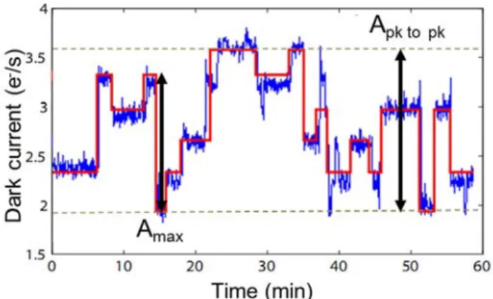
The presented analysis focuses on the transition maximum amplitude. This parameter appears to be efficient for distinguishing the DC-RTS type [9]-[11]. As can be seen in Fig. 1, the transition maximum amplitude, Amax, corresponds
to the maximum amplitude between two transitions. It is important to note that in the case of multi-level RTS, this amplitude may differ from the peak to peak amplitude. Amax is
only related to the defect with the highest generation rate change whereas Apk to pk is related to all RTS defects in the
pixel and mixes the different generation rate changes. In this study, Amax is chosen as the parameter of interest to focus on
the worst-impacting defect in the pixel.
Fig. 1. Example of time behavior of a DC-RTS pixel, obtained after neutron exposure, representing transition maximum amplitude (Amax) and peak to peak amplitude (Apk to pk) during a one hour observation. In cases of multi-level DC-RTS due to one or several metastable defects, peak to peak amplitude could take into account several DC-RTS centers whereas transition maximum amplitude is associated with only one defect.
> REPLACE THIS LINE WITH YOUR PAPER IDENTIFICATION NUMBER (DOUBLE-CLICK HERE TO EDIT) < 3
Fig. 2. Illustration of the DC-RTS transition maximum amplitude histogram. The detection threshold of the method is represented at the beginning of the histogram. The parameters of the exponential law are also illustrated. k.λ corresponds to the Y-axis intersection and λ corresponds to the slope in this semi-log plot.
Fig. 2 illustrates a typical distribution of the transition maximum amplitude. The initial part of the distribution (colored area in Fig. 2) decreases due to the use of a detection threshold. The distribution can then usually be fitted using the exponential law:
f(x)=k⋅λ⋅exp(−λ⋅x) (1) where 1/λ is the mean value of the distribution and corresponds to the specific signature of the DC-RTS type [10].
k is related to the number of pixels in the array and to the
concentration of RTS centers. This k parameter could be expressed as:
k =Cdef ⋅b⋅Npix⋅A (2) where Cdef is the number of detected RTS defect (per volume, Cvol or per surface, Csurf), b is the bin size of the histogram, Npix is the number of pixels in the studied array and A is the
volume or surface of interest. This factor corresponds to the depleted volume, Vdep, when the phenomenon is related to
metastable bulk defects and it is the surface of the depleted interface, Sint, when the phenomenon is related to interface
state. The exponential distribution is usually used to describe the time between events in a Poisson process but it is found in various other contexts. This law therefore seems appropriate for the distribution of RTS amplitudes, which is related to the distribution of metastable defects in the pixel array. In the next section, we focus on the exponential law parameters obtained for different materials, different types of irradiation and different technologies in order to observe potential common behavior and to provide common parameters to predict DC-RTS distribution.
IV. DC-RTS IN SILICON-BASED IMAGERS
Silicon is the most commonly used material for solid state image sensors. In this section, two different device technologies are studied, CCD and CIS. For CIS, we focus on
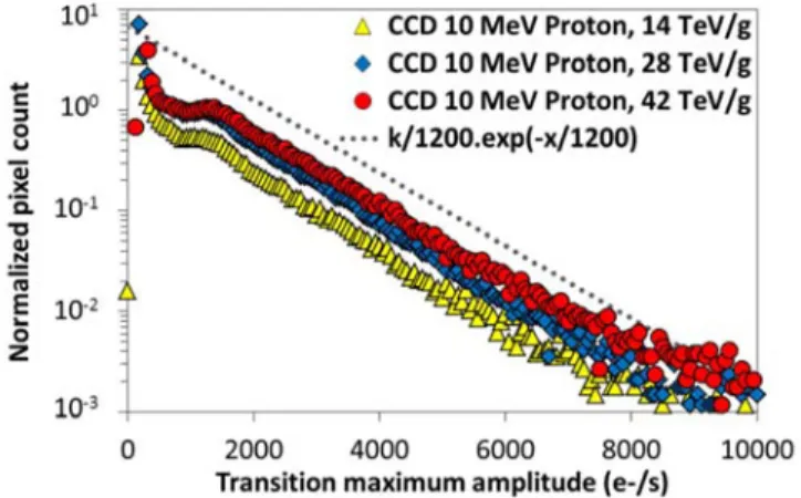
Fig. 3. DC-RTS transition maximum amplitude histograms for CDD after 10 MeV proton irradiation at several fluences.
the latest generation devices using Pinned PhotoDiodes (PPD). Although some of the measurements presented here have already been published [9]-[11], they are studied in more details and new sets of data from other foundries and technologies are added to the analysis.
A. DC-RTS in Charge Coupled Devices
CCD are sufficiently mature for scientific application and are used in most space missions. As with other imaging technologies, CCDs are sensitive to the radiations and show an increase in DC-RTS after irradiation.
The investigated device is a frame transfer CCD having 1024×1024, 13 µm square pixels, irradiated with 10 MeV protons at three different fluences. The device is operated in inverted mode to suppress the dark current caused by the native and TID-induced defects located at Si/SiO2 interfaces.
Fig. 3 shows the distribution of DC-RTS transient maximum amplitude for the three studied fluences. The exponential curve is also plotted using a mean value of 1200 e-/s corresponding to those previously reported for CISs based on conventional photodiodes [11]. As can be seen in the figure, this average value of 1200 e-/s fits well the CCD data, meaning that both CIS and CCD technologies share a common behavior regarding Dd-induced RTS. The beginning of the
experimental distribution exhibits an unexpected shape, but as this behavior was not observed in previous studies focusing on CCDs [4], [5], we are unable yet to draw any conclusion about this behavior.
B. DC-RTS in CMOS image sensors
The CMOS image sensor (CIS) market has been continuously growing for the last two decades and CIS is now becoming the most sustainable technology for future space imaging applications. The radiation response of this technology has been widely studied for various radiation environments [12]-[17] and CIS are now used for several space imaging applications, such as star trackers, microcamera exploration and even geostationary Earth imaging.
However, DC-RTS behavior is not fully understood, especially for PPD CIS. In this section, we focus on both CIS using conventional photodiodes and CIS using pinned photodiodes.
> REPLACE THIS LINE WITH YOUR PAPER IDENTIFICATION NUMBER (DOUBLE-CLICK HERE TO EDIT) < 4
Fig. 4. DC-RTS transition maximum amplitude histograms for CIS1 (using conventional photodiode) after proton and neutron irradiations at several fluences.
Fig. 5. DC-RTS transition maximum amplitude histograms for CIS1(using conventional photodiode) after X-ray and γ-ray irradiations for several doses.
1) Conventional Photodiodes
DC-RTS in CMOS image sensors using conventional photodiodes, also called 3T pixel CIS, has been previously studied in [6], [9]-[12]. These studies consider two types of DC-RTS. The first one is related to displacement damage and occurs after neutron and proton irradiations. This DC-RTS is characterized by large amplitudes between transitions and generally consists of multiple levels [11]. The second type is related to TID [9] and occurs after X-ray, Co-60 γ-ray and proton irradiations. This DC-RTS is characterized by a RTS pixel exhibiting bi-level and small amplitudes [10].
Fig. 4 shows the amplitude distributions after neutron and proton irradiation at different fluences. The first interesting point concerns the exponential behavior of the data which seems close to the one observed for previous results. The average value of 1200 e-/s previously observed for other CIS devices [10], [11] also gives satisfactory results for this data set. The second important point concerns the proportionality of the effect with Dd. Indeed, for the same Dd the data are
superimposed, regardless of the type of incident particle (protons or neutrons) used for irradiation. Another previously observed point concerns the peak located at the beginning of each proton curve. This effect is attributed to TID-induced DC-RTS [10] explaining that it is not observed for neutrons because of the negligible associated TID. A new exponential curve using a mean value of 110 e-/s is plotted in the figure to
Fig. 6. 3T pixel cross-section from a conventional photodiode using STI (CIS1). The space charge region is in contact with the lower part of the STI.
Fig. 7. 3T pixel cross-section from a conventional photodiode using recessed STI layout (CIS2). The space charge region is in contact with the Pre-Metal Dielectric oxide layer.
highlight the agreement. This value comes from [9], in which the authors focused on TID-induced DC-RTS. We note a good agreement between this exponential curve and the proton data. This confirms that proton-induced DC-RTS is related to both TID and Dd.
Fig. 5 shows previously published data for X-ray and γ-ray irradiation. The exponential distribution with a mean of 110 e -/s is also added and agrees well with the data. It is interesting to note that even un-irradiated devices exhibit this exponential behavior. These results confirm that the TID effect is similar after proton, X-ray and γ-ray irradiations, being due to metastable interface state defects located at Si/SiO2 interfaces.
Indeed, Shallow Trench Isolations (STI) are used in this technology and are known to be related to TID-induced dark current increase in CIS [18]. The metastable interface states responsible for the observed DC-RTS are thus probably located at the interface between the depleted region of the photodiode and the STI. To confirm this statement, two typesof CIS were designed using the layout variations depicted in Fig. 6 and Fig. 7. In the Fig. 6 design, the space charge region is in contact with the STI while in Fig. 7, the STI are recessed away from the photodiode active region, implying that the space charge region is in contact with the Pre-Metal Dielectric (PMD) layer. The PMD is also a silicon oxide but its properties differ from those of the STI. Fig. 8 shows the distribution of amplitudes for the same γ-ray dose deposited on the two layouts. We observe a clear difference between the results. When the space charge region is in contact with the PMD, there is an order of magnitude decrease in the number of detected RTS (whereas the average amplitude seems similar) compared with when it is in contact with the STI. This means that TID-induced metastable interface state buildup is more intense in STI than in PMD. This phenomenon could be explained by the difference between the STI and PMD oxide processes. Previous studies [19] show that the interface state density increase with TID is
> REPLACE THIS LINE WITH YOUR PAPER IDENTIFICATION NUMBER (DOUBLE-CLICK HERE TO EDIT) < 5
Fig. 8. DC-RTS transition maximum amplitude histograms for CIS1 and CIS2 (using conventional photodiode) after γ-rays. The TID reaches 30 krad(SiO2) for both devices.
faster at STI interfaces than at PMD ones. Therefore, the recessed STI layout mitigates significantly the TID-induced DC-RTS phenomenon. The most important point for this study concerns the exponential behavior of both curves. If we add the exponential curve using 110 e-/s as mean value, we note that metastable interface states located in the STI and in the PMD have the same exponential signature. These results imply that the metastable centers have the same generation rates and we can assume that they are also associated to the same defect structures.
2) Pinned Photodiodes
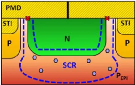
The pinned photodiode CIS is the most widely-used image sensor, carried in almost every pocket, as this technology is used for mobile phone cameras. This technology is particularly promising for scientific applications because it benefits from all the recent process improvements in terms of quantum efficiency, noise and dark current. The main difference between PPD CIS and older 3T pixel technology is the addition of a fourth transistor and a pinned photodiode. Consequently it is also called 4T pixel architecture. The operation of such device is explained in [20]. As can be seen in Fig. 9, the device has a buried space charge region and therefore no obvious contact with any isolation oxide. However, to really have a buried depleted volume during the sensor exposure time, the additional transistor, called the transfer gate, should be accumulated [21]. If this is not the case, that is to say, if we polarize the transfer gate to 0V during the exposure time, the space charge region will extend under the gate and the interface states located in the STI surrounding the gate (see Fig. 9) will participate in the dark current generation mechanism. Moreover, these defects can be metastable and can induce DC-RTS. It should be emphasized that an additional transfer gate, such as an anti-blooming or global shutter gate can also induces an interface state DC-RTS if they are not accumulated (which is always the case for anti-blooming gates [22]).
Fig. 10 shows the RTS amplitude histograms for PPD CIS from three different foundries, after γ-ray irradiation. This figure is thus dedicated to TID effects. We plot the exponential curves using the two generic average values, 110 e-/s and 1200 e-/s. It can clearly be seen that the lower average value (110 e-/s), related to TID, is in fairly good agreement
Fig. 9. 4T pixel cross section through the pinned photodiode and transfer gate. The cross sections of the three insets correspond to the photodiode/transfer gate area for different polarizations and for the side view. This latter inset shows the contact between the space charge region and the STI when transfer gate is polarized at 0V.
Fig. 10. DC-RTS transition maximum amplitude histogram for several PPD CISs after Co-60 γ-ray irradiation. Common behavior is observed for the three different foundries.
with the data. As expected for γ-ray irradiation, the 1200 e-/s average value related to Dd is not working well here. The
results confirm on PPD CIS the common behavior of this average value for TID-induced DC-RTS in silicon-based material. Un-irradiated devices using accumulation bias are not represented in the figure because they do not exhibit any DC-RTS behavior. For the higher doses, the large amplitudes differ from the exponential curve (and thus from the 110 e-/s average value typical for TID-induced DC-RTS). One hypothesis could be the presence of a high electric field in this device that would enhance the DC-RTS amplitude and thus generate a high amplitude distribution tail.
Fig. 11 shows the amplitudes obtained after neutron and proton irradiations for two foundries. Although the statistics are not sufficient to be definitive, we also plot the two exponential curves. The results seem to correlate with the 1200 e-/s value. This implies that metastable defects are located in the silicon bulk of the space charge region. An
> REPLACE THIS LINE WITH YOUR PAPER IDENTIFICATION NUMBER (DOUBLE-CLICK HERE TO EDIT) < 6
Fig. 11. DC-RTS transition maximum amplitude histogram for several PPD CISs after proton and neutron irradiations.
increase at the beginning of the distribution which appears for proton irradiation could be related to TID effects.
All the results presented in this section emphasized the common behavior of DC-RTS in silicon-based devices. Two exponential average values seem sufficient to fit the different types of irradiation: 110 e-/s for the DC-RTS related to TID and 1200 e-/s for the DC-RTS related to displacement damage.
V. DC-RTS IN INFRARED IMAGERS
Silicon is not the only material of interest for imaging applications. For the infrared range, other semiconductors are used. In this section we investigate two types of detectors based on different materials.
A. HgCdTe-based imagers
The first device is based on a heterojunction of Mercury Cadmium Telluride (MCT), also called an HgCdTe sensor. It offers very good performance in the infrared range and its wavelength response be tuned by varying the proportion of each component. However, this detector has to be cooled to a temperature below 200 K in order to reduce the thermal dark current and reach acceptable efficiency. The device under study is illustrated in Fig. 12. The HgCdTe active layer is grown on a ZnCdTe substrate. The N+ area of the N+/P photodiode is doped with In or B. A bump bonding is used to connect the cathode to the CMOS readout circuit [23]. Although this device is not irradiated, we choose to present its results because, to the best of our knowledge, this is the first time that DC-RTS amplitudes are reported in such a device that is today considered for space mission where the radiation environment is known to creates defects inducing dark current [23], [24] and DC-RTS in other technologies.
Fig. 13 shows the amplitude distributions for two different cooling procedures of the same device. The measurement temperature is the same in both cases (below 200 K). Although un-irradiated, this device also demonstrates exponential behavior. The exponential curve is plotted in the figure using the most favorable average value to reproduce the experimental data (210 e-/s). The results are close to the average value observed for TID in silicon. However, the testing temperature is below 200 K meaning that the average
Fig. 12. Pixel cross section of the Mercury Cadmium Telluride device. The photodiode is N+/P.
Fig. 13. DC-RTS transition maximum amplitude histogram for MCT devices following two cooling procedures.
value can be higher at ambient temperature (under the assumption that the DC-RTS amplitude is proportional to the temperature in HgCdTe material). If we assume an activation energy of the DC-RTS amplitude near the mid-gap value of the material (as for DC-RTS in silicon devices), we obtain an average value around 400 ke-/s, which is two orders of magnitude higher than in silicon. It is interesting to note here that the behavior is still exponential even though the defects are obviously different from those observed in silicon-based materials.
B. InGaAs-Based Imagers
While the best performance detectors for infrared detection in the 1 µm to 15 µm range tend to be developed using HgCdTe technology, these detectors have to be cooled in order to reach acceptable performance. Other technologies allow to avoid this problem. For example, the Indium Gallium Arsenide technology presents a natural cutoff wavelength around 1.65 µm, which makes it suitable for detection in the Short Wavelength InfraRed (SWIR) spectral range. A major advantage of this technology concerns the operating temperature, which can be above 230 K. This relaxes the thermal constraints for the application. Consequently, InGaAs-based imagers also appear as suitable candidates for numerous space missions [7], [25].
> REPLACE THIS LINE WITH YOUR PAPER IDENTIFICATION NUMBER (DOUBLE-CLICK HERE TO EDIT) < 7
Fig. 14. Pixel cross section of the InGaAs device. TheInGaAs active layer is grown on InP N-doped substrate. Zn diffusion is used in the InP cap layer to obtain the P+/N photodiode. The space charge region extends into the InGaAs active layer.
Fig. 15. DC-RTS transition maximum amplitude histogram for InGaAs device for three temperatures.
The device studied here uses InGaAs grown on an InP N-doped substrate. This substrate is used because it exhibits the lowest density of defects [25]. An N-doped InP layer with 1 µm thickness is grown on the active layer. P doping is obtained using Zn diffusion in the cap layer. Fig. 14 presents a cross section of the 30 µm pitch pixel showing the space charge region of the P+/N photodiode. The array consists of 320×256 pixels. This device was irradiated using protons in order to evaluate its behavior in a space-like radiation environment.
Fig. 15 shows the distribution of RTS transition maximum amplitudes at different temperatures for InGaAs detector. This environment parameter is investigated to observe the induced variations in distribution shape. At ambient temperature, the distribution also shows exponential behavior but the average value of the exponential curve that best fits the data is 250 ke-/s. This is two orders of magnitude higher than the value obtained for silicon, meaning that the defects related to DC-RTS in such material have a higher generation rate. Then, means that the DC-RTS phenomenon is highly active in InGaAs-based material and its amplitude may be a serious issue for space instruments. The measurements at lower temperatures show that average values of the exponential curves decrease with temperature. The estimated activation energy is near the mid-gap value. This result should be observed over a larger temperature range and could be used to
Fig. 16. Extraction of the defect concentration due to displacement damage. The power law is used to fit the data and the power factor obtained is 1.01 meaning that the distribution is linear.
predict the DC-RTS amplitudes in a particular radiation environment.
VI. DISCUSSION
A. DC-RTS related to material types
We observed DC-RTS in the three investigated materials. In order to discuss these results, we used Equation (2) to extract the number of detected metastable center in each device, as explained in [11]. The method consists in extrapolating the exponential curve and estimating the Y-axis intercept. As explained in Fig. 2, this intercept corresponds to k.λ using Equation (1). Therefore, dividing the Y-axis intercept by λ, b,
Npix and A (here A corresponds to the depleted volume because
we investigated the Dd-induced DC-RTS related to the bulk
metastable defects), gives the number of detected metastable defect (cm-3). It is important to note that for protons, two exponential behaviors are observed. Therefore, the concentration of bulk defects related to Dd is obtained using
the Y-axis intercept of the exponential distribution corresponding to displacement damage (with λ = 1200 e-/s). The other TID-related exponential behavior is mentioned in the next sub-section (B) in order to estimate the metastable interface states along the Si/SiO2 interfaces. It is important to
mention that the number of detected metastable center corresponds to the metastable defect concentration if there is a maximum of one metastable center per pixel. For the Dd
investigated in space radiation studies, we assume that the maximum number of detected RTS center is close to one per pixel, therefore, we name this number as “metastable defect concentration”.
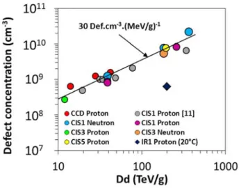
Fig. 16 gives the changes in metastable defect concentration per microvolume when the DC-RTS is known to be related to displacement damage. Using two silicon-based technologies and five foundries we find a metastable defect concentration of around 30 metastable defects / cm3 / (MeV/g) in silicon at 23°C. This value is slightly lower than the one reported in previous work [11]. This small difference could be explained
> REPLACE THIS LINE WITH YOUR PAPER IDENTIFICATION NUMBER (DOUBLE-CLICK HERE TO EDIT) < 8
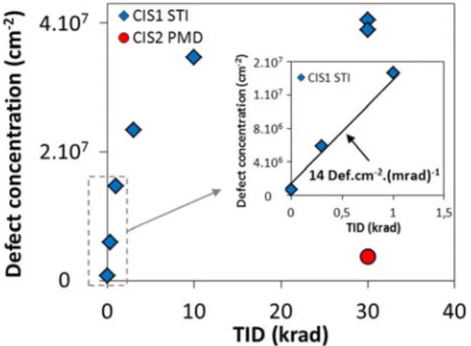
Fig. 17. Extraction of defect concentration due to TID. In this case the concentration is provided in (cm-2) because the interface states are localized along the surface between the space charge region and the isolation oxides.
by the fact that previous study estimated the photodiode volume through C-V measurements on large test structures whereas we used here Technology Computer-Aided Design (TCAD) simulations that are considered to be more accurate than C-V measurements in this case. We measured the doping profiles of the photodiode using Secondary Ion Mass Spectroscopy (SIMS) and included them in the TCAD simulation in order to extract an accurate estimation of the depleted volume. Data from [11] are corrected using depletion width of 2 µm instead of 1.16 µm in [11] and plotted in the figure. The proton energy of these data ranges from 7 MeV to 180 MeV.
The InGaAs device is also plotted in the figure to emphasize the difference between materials. The defect concentration is around 3 metastable defects / cm3 / (MeV/g) at 20°C. This value is clearly lower than for silicon, meaning that a higher displacement damage dose level is needed to create metastable defects in InGaAs than in silicon. However, the mean maximum RTS transition amplitude in InGaAs is significantly higher than in silicon.
B. DC-RTS related to Si/SiO2 interface types
The same extraction method is applied to DC-RTS related to TID. In this case, the exponential distribution with an average value around 110 e-/s is used to extract the metastable interface state concentrations (here the A of Equation (2) corresponds to Sint and the concentration is expressed in cm-2).
The results are presented in Fig. 17. The dose dependence of the defect concentration is clearly non-linear for the defects located close to the STI interface. This behavior could be attributed to a saturation of the exponential method. When almost all pixels are RTS pixel, the number of detected RTS pixel saturates. However, an inset focusing on the first part of the curve is added to show the behavior for low TID. For these low dose data, the increase of defect concentration seems linear with TID. The linear fit gives a concentration of 14 defects per cm-2 and per mrad(SiO2).
VII. CONCLUSION
This paper analyzes DC-RTS in several solid-state image sensors. The DC-RTS related to displacement damage and to metastable bulk defects is investigated in three materials. We observed common behavior in silicon devices, even when different technologies are used. The factors extracted from the analysis at 23°C should be verified in even more devices to confirm the apparent universal behavior observed in this study. It appears that these parameters can be used, without any parameter adjustment or preliminary measurement, to predict DC-RTS behavior caused by displacement damage in silicon-based devices operating in a radiation environment. The results obtained from InGaAs infrared imagers need to be confirmed by assessment of further devices. Although HgCdTe devices were un-irradiated, it is important to report that DC-RTS exists in such devices and that the transition maximum amplitude behavior is exponential. As this material is a potential component of future space missions, work is on-going to give more details about DC-RTS in these detectors. DC-RTS related to total ionizing dose is also being studied further. The factors extracted using the exponential law show similarities in several isolation oxides. The metastable interface states located close to STI and PMD present the same generation rate and seem to be associated to the same defect structure. Finally, we propose some mitigation techniques to reduce the impact of the DC-RTS related to TID by using a recessed STI design.
The method developed, based on exponential distribution, seems to be a useful tool for characterizing DC-RTS in solid-state imagers. The use of exponential distribution is straight forward to implement and enables easy prediction of the generation of DC-RTS defects. Further measurements are on-going to support this method, especially in devices currently in-flight and integrated in satellite payloads.
ACKNOWLEDGMENT
The authors would like to thank the ISAE Image Sensor Team for their help, especially Franck Corbière and Philippe Martin-Gonthier for the sensor design, Paola Cervantes, Magali Estribeau and Barbara Avon for their help with measurements and Sebastien Rolando for his critical assessment of the study. They would also like to thank Marc Gaillardin, Sebastien Quenard, Yves Leo, CEA, Mathieu Boutillier, CNES and Guy Berger, UCL, for their assistance during neutron and proton irradiations. Final thanks go to Jérémy Baer, Emma Martin and Lionel Roucayrol for their assistance during data analysis.
REFERENCES
[1] J.R. Srour, R.A. Hartmann and K.S. Kitazaki, “Permanent damage produced by single proton interactions in silicon devices,” IEEE Trans. Nucl. Sci., vol. NS-33, no. 6, pp. 1597–1604, Dec. 1986.
[2] P.W. Marshall, C.J. Dale, E.A. Burke, G.P. Summers and G.E. Bender, “Displacement damage extremes in silicon depletion regions,” IEEE Trans. Nucl. Sci., vol. 36, no. 6, pp. 1831–1839, Dec. 1989.
[3] I. H. Hopkins and G. R. Hopkinson, “Random telegraph signals from proton-irradiated CCDs,” IEEE Trans. Nucl. Sci., vol. 40, no. 6, pp. 1567–1574, Dec. 1993.
> REPLACE THIS LINE WITH YOUR PAPER IDENTIFICATION NUMBER (DOUBLE-CLICK HERE TO EDIT) < 9
[4] I. H. Hopkins and G. R. Hopkinson, “Further measurements of random telegraph signals in proton irradiated CCDs,” IEEE Trans. Nucl. Sci., vol. 42, no. 6, pp. 2074–2081, Dec. 1995.
[5] T. Nuns, G. Quadri, J.-P. David, O. Gilard, and N. Boudou, “Measurements of random telegraph signal in CCDs irradiated with protons and neutrons,” IEEE Trans. Nucl. Sci., vol. 53, no. 4, pp. 1764– 1771, Aug. 2006.
[6] G. R. Hopkinson, “Radiation effects in a CMOS active pixel sensor,” IEEE Trans. Nucl. Sci., vol. 47, no. 6, pp. 2480–2484, Dec. 2000. [7] G. R. Hopkinson, “Radiation effects in InGaAs and microbolometer
infrared sensor arrays for space applications,” IEEE Trans. Nucl. Sci., vol. 55, no. 6, pp. 3483–3493, Dec. 2008.
[8] A.L. D’Souza, M.G. Stapelbroek, E.W. Robinson, C. Yoneyama, H.A. Mills, M.A. Kinch, M.R. Skokan and H.D. Shih, “Noise attributes of LWIR HDVIP HgCdTe detectors,” IEEE J. Elec. Mat., vol. 37, no 9, pp 1318-1323, Sep. 2008.
[9] V. Goiffon, P. Magnan, P. Martin-Gonthier, C. Virmontois and M Gaillardin, “Evidence of a novel source of random telegraph signal in CMOS image sensors,” IEEE Electron Devices Letter, vol. 32, no. 6, Jun. 2011.
[10] C. Virmontois, V. Goiffon, P. Magnan, O. Saint-Pé, S. Girard, S. Petit, G. Rolland and A. Bardoux, “Total Ionizing Dose Versus Displacement Damage Dose Induced Dark Current Random Telegraph Signals in CMOS Image Sensors,” IEEE Trans. Nucl. Sci., vol. 58, no. 6, pp. 3085–3094, Dec. 2011.
[11] V. Goiffon, P. Magnan, O. Saint-Pé, F. Bernard, and G. Rolland, “Multi level RTS in proton irradiated CMOS image sensors manufactured in a deep submicron technology,” IEEE Trans. Nucl. Sci., vol. 56, no. 4, pp. 2132-2141 Aug. 2009.
[12] J. Bogaerts, B. Dierickx, and G. Meynants, "Enhanced dark current generation in proton-irradiated CMOS active pixel sensors," IEEE Trans. Nucl. Sci., vol. 49, no. 3, pp. 1513-1521, Jun. 2002.
[13] G. R. Hopkinson, “Radiation effects in a CMOS active pixel sensor,” IEEE Trans. Nucl. Sci., vol. 47, no. 6, pp. 2480-2484, Dec. 2000. [14] J. Bogaerts, B. Dierickx, and G. Meynants, “Enhanced dark current
generation in proton-irradiated CMOS active pixel sensors,” IEEE Trans. Nucl. Sci., vol. 49, no. 3, pp. 1513-1521, Jun. 2002.
[15] J. Bogaerts, B. Dierickx, G. Meynants, and D. Uwaerts, “Total Dose and Displacement Damage Effects in a Radiation-Hardened CMOS APS,” IEEE Trans. Electron Dev., vol. 50, no. 1, pp. 84-90, 2003.
[16] G. R. Hopkinson, “Radiation Effects on a radiation-tolerant CMOS Active Pixel Sensor,” IEEE Trans. Nucl. Sci., vol. 51, no. 5, pp. 2753-2762, Dec. 2004.
[17] M. Beaumel, D. Herve, and D. Van Aken. “Cobalt-60, proton and electron irradiation of a radiation-hardened active pixel sensor,” IEEE Trans. Nucl. Sci., 57, no. 4, pp. 2056-2065, Aug. 2010.
[18] V. Goiffon, P. Magnan, O. Saint-Pé, F. Bernard, and G. Rolland, “Total dose evaluation of deep submicron CMOS imaging technology through elementary device and pixel array behavior analysis,” IEEE Trans. Nucl. Sci., vol. 55, no. 6, pp. 3494-3501, Dec. 2008.
[19] M. Gaillardin, V. Goiffon, C. Marcandella, S. Girard, M. Martinez, P. Paillet, P. Magnan, and M. Estribeau, “Radiation effects in CMOS isolation oxides: differences and similarities with thermal oxides,” IEEE Trans. Nucl. Sci., vol. 60, no. 4, pp. 2623–2629, Aug. 2013.
[20] P. Lee, R. Gee, M. Guidash, T. Lee, and E. R. Fossum, “An active pixel sensor fabricated using CMOS/CCD process technology,”in Proc. IEEE Workshop CCDs Adv. Image Sens., 1995, pp. 115–119.
[21] T. Watanabe, J.-H. Park, S. Aoyama, K. Isobe, and S. Kawahito, “Effects of negative-bias operation and optical stress on dark current in CMOS image sensors,” IEEE Trans. Electron Devices, vol. 57, no. 7, pp. 1512–1518, Jul. 2010.
[22] E. Martin, T. Nuns, C. Virmontois, J-P. David and O. Gilard, “Proton and γ-rays irradiation-induced dark current random telegraph signal in a 0.18-µm CMOS image sensor,” IEEE Trans. Nucl. Sci., vol. 60, no. 4, pp. 2503–2510, Aug. 2013.
[23] A. Weber, W. Belzner, L.-D. Haas, S. Hanna, K. Hofmann, A. Neef,M. Reder, P. Stifter, J. Wendler, J. Ziegler, and H.-P. Nothaft, “Radiation hardness of two-dimensional focal plane detector arrays for LWIR/VLWIR space sounding missions,” in Proc. of RADECS, pp 336–339, 2011.
[24] C.J. Marshall, P.W. Marshall, C.L. Howe, R.A. Reed, R.A. Weller, M. Mendenhall, A. Waczynski, R. Ladbury, and T.M. Jordan, “Comparison of measured dark current distributions with calculated damage energy distribution in HgCdTe,” IEEE Trans. Nucl. Sci., vol. 54, no. 4, pp. 2623–2629, Aug. 2007.
[25] A. Rouvié, J-L Reverchon, O. Huet, A. Djedidi, J-A Robo, J-P Truffier, T. Bria, M. Pires, J. Decobert, and E. Costard, “InGaAs focal plane array developments at III-V Lab, ” Proc. SPIE 8353, Infrared Technology and Applications, vol. 835308, May 2012.