HAL Id: hal-00804184
https://hal.archives-ouvertes.fr/hal-00804184
Submitted on 25 Mar 2013HAL is a multi-disciplinary open access archive for the deposit and dissemination of sci-entific research documents, whether they are
pub-L’archive ouverte pluridisciplinaire HAL, est destinée au dépôt et à la diffusion de documents scientifiques de niveau recherche, publiés ou non,
Buried Anti Resonant Reflecting Optical Waveguide
based on porous silicon material for an integrated Mach
Zehnder structure
Mohamed Hiraoui, Mohammed Guendouz, Nathalie Lorrain, Lazhar Haji,
Mehrezi Oueslati
To cite this version:
Mohamed Hiraoui, Mohammed Guendouz, Nathalie Lorrain, Lazhar Haji, Mehrezi Oueslati. Buried Anti Resonant Reflecting Optical Waveguide based on porous silicon material for an integrated Mach Zehnder structure. Applied Physics Letters, American Institute of Physics, 2012, 101 (19), pp.191114. �10.1063/1.4766729�. �hal-00804184�
Buried Anti Resonant Reflecting Optical Waveguide
based on porous silicon material for an integrated Mach Zehnder structure
M. Hiraoui,1,2 M. Guendouz,1,a), N. Lorrain,1 L. Haji1 and M. Oueslati2 1)
Université Européenne de Bretagne, CNRS-UMR FOTON 6082, BP 80518,
ENSSAT 6 rue Kerampont, 22305 Lannion Cedex, France
2)
Unité de Spectroscopie Raman, Faculté des Sciences de Tunis, 2092 El Manar-Tunisia.
A buried Anti Resonant Reflecting Optical Waveguide for an integrated Mach
Zehnder structure based on porous silicon material is achieved using a classical
photolithography process. Three distinct porous silicon layers are then elaborated in a
single step, by varying the porosity (thus the refractive index) and the thickness while
respecting the anti-resonance conditions. Simulations and experimental results
clearly show the antiresonant character of the buried waveguides. Significant
variation of the reflectance and light propagation with different behavior depending
on the polarization and the Mach Zehnder dimensions is obtained. Finally, we
confirm the feasibility of this structure for sensing applications.
Integrated optical devices are frequently used for communications1 and biochemical
applications.2 In the last decade, optical interferometry3,4 is an evolving field which has been
adopted for sensing applications. The Mach Zehnder (MZ) configuration appears to be the most
widely used device in the field of biosensors thanks to its easy design and fabrication.5 Recently,
MZ interferometers using various materials for chemical or biochemical sensing applications
have been developed.6-9 In these MZ structures, the molecules to be detected are adsorbed at the
surface of the interaction zone of the sensing arm and so will interact only with the evanescent
field.10 Differentkinds of resonant or antiresonant waveguides constituting the MZ structure can
be constructed.5,11
Porous silicon12 is an attractive and promising material which can be used in the
fabrication of MZ interferometers for biosensing applications. The porosity and thus the
refractive index can be easily varied as well as the thickness of the distinct porous layers of the
structure. Moreover, the large internal specific area of the porous silicon layer is an asset in
improving the sensitivity of the biosensor. Indeed, other porous structures have already been
used to increase the sensitivity of waveguide based biosensors.13,14
Recently, we have demonstrated the feasibility of a planar AntiResonant Reflecting
Optical Waveguide (ARROW) based on porous silicon for detection purposes even if the
refractive index contrast is rather low15,16 compared to other materials.17,18
The particular characteristic of this antiresonant waveguide is that the upper porous layer
performs both the role of active and guiding layer supporting field propagation which ensures a
more sensitive interaction between the propagated light and the infiltrated biological species.
which can be easily used with porous silicon material. Indeed, buried resonant waveguides based
on porous silicon have been already demonstrated for telecommunication applications.19,20
In this work, we studied the integration of buried ARROW based on porous silicon in MZ
structures used as optical transducers for biosensor applications. The propagation and modal
characteristics of light in the waveguides and then in the MZ structure were investigated. We
showed that the propagation of light was almost the same for both arms of the MZ structure. In
order to realize a buried optical waveguide which is the main element of the interferometer MZ
and to achieve a biosensor application, the structure must satisfy several conditions. These
include the preparation of the porous layers with defined properties and the choice of the
dimensions of the mask used. These parameters affect light propagation behavior with single or
multi mode character and also the resonant or antiresonant effect.
The two arms of the MZ structures we fabricated consist of two buried waveguides, with
lengths varying from 4 to 6 mm, separated by a distance of 90 µm and connected by S bends
having a curvature radius of 5 mm. The width of the waveguide apertures varies between 4 and
20 µm. The schematic and dimensions of the MZ structure are summarized in Fig. 1(a). The MZ
structure was made using a photolithography process, performed on a heavily P doped (100)
silicon substrate with a resistivity of 7 m1.cm, with a well defined mask designed using
Olympios software. After photolithography step, an electrochemical anodization process was
performed through the mask apertures to create three distinct porous silicon layers with
porosities and thicknesses satisfying the antiresonance conditions21 to obtain the ARROW
structures.15,16 For this anodization process, we used an electrolyte composed of HF (50 %),
ethanol and deionised water (at 18 M1) solution with ratios of 2-2-1 respectively. We applied
layer (dc) which has the lowest refractive index (nc = 1.65 ± 0.06) was created. Then the first
cladding layer (d1) with high refractive index (n1 = 2.95 ± 0.06) was made and this was followed
by a second cladding layer (d2) with a lower refractive index (n2 = 2.07 ± 0.06) than the previous
one. The porosities and refractive indices are deduced from reflectance spectra using the
Bruggeman model.22
SEM top view and cross section micrographs of the buried ARROW in the MZ structure
with a width of 4 µm, are presented in Figs. 1(b) and 1(c) respectively. From the SEM top view
we can clearly observe the two defined buried waveguides constituting the two arms of the MZ
structure with a spacing of 90 2m. The cross section image of the waveguide clearly shows the
three different porous silicon layers of the structure and their measured thicknesses. The
waveguide appears as a half cylinder shape due to the anisotropy of the formation process related
to the silicon crystallographic orientations.23,24
FIG. 1. Schematic and characteristic features of the MZ structure (a), SEM top view (b) and
cross section (c) micrographs of the buried waveguides which compose the MZ structure. The
In the case of an ARROW structure, unlike conventional waveguides, the light is confined in the core layer by total internal reflection at the upper air/core layer interface and by anti-resonant reflection due to the presence of the cladding layers underneath the core layer. The refractive index of the first cladding layer must be higher than those of the core and second cladding layer. The ARROW structure can therefore be considered as a leaky waveguide with radiation losses within the substrate reduced by the high reflection obtained by choosing the required thickness of the cladding layers.21
For a given thickness of the core layer dc, the optimum thicknesses (d1 and d2) of the two
cladding layers for the mth mode and for the Mth order of the antiresonant conditions must satisfy
the following relationship21:
1 2 2 2 1,2 1,2 1,2 1,2 ( 1) 1 .(2 1) 4 2 c c n m d M n n n d λ 1 3 4 3 + λ4 2− 5 6 = −77 88 +77 88 + 5 9 A 9 A 6 B C M, m = 0, 1, 2, …
Where 3 (1.55 µm) is the light propagation wavelength along the z direction. In our case, we
only have considered the fundamental mode (m = 0) which corresponds to a single mode
propagation.
The reflectivity (R) at the interface between the core and the first cladding layer is a key parameter for an ARROW structure. The reflectivity expression for any polarization (TE or TM) is obtained by calculations based on the Fresnel coefficients.25 Using these, R was calculated16 and plotted in Fig. 2 for both TE and TM polarizations as a function of d1 for
FIG. 2. Calculated reflectivity as a function of d1 for dc = 4.3 µm for both TE and TM
polarizations, with fixed experimental refractive index values nc = 1.65 ± 0.06, n1 = 2.95 ± 0.06,
n2 = 2.07 ± 0.06 and at a working wavelength of 3 = 1.55 µm.
From this figure, we see that the maximum reflectivity (Rmax 4 0.85) for the TE mode is obtained
for values of d1 around 0.5 µm corresponding to the first order of the anti-resonance conditions.
In the case of the TM mode, we note that the reflectivity is low and also that the difference
between the maximum and minimum of reflectivity is lower than for the TE mode. This
distinction in the reflectivity between the TE and TM modes clearly reflects the feature of the
ARROW structure.21 The experimental thickness of the first cladding layer measured by SEM
was about 0.5 µm (Fig. 1(c)), a value which corresponds to a maximum of the reflectivity
according to Fig. 2. Thus, the antiresonant conditions are respected in the buried waveguides
constituting the MZ structure.
Furthermore, the Beam Propagation Method (BPM)26 was used to simulate the field
experimental values of the refractive index and thickness. In Fig. 3, we present the cross section
images of the light propagated along the z direction of the 10 mm length ARROW structure for
both TE (Figs. 3(a) and 3(c)) and TM (Fig. 3(b) and 3(d)) polarizations. Also, the profiles of the
field measured in the vertical direction at the input (start field) and at the output (end field) of the
waveguide are reported. The estimated boundaries of the three layers are indicated by the dashed
lines.
FIG. 3. Cross section images of the light propagated along the z direction and simulated near
field profiles of the ARROW structure for TE (a, c) and TM (b, d) polarizations with the
following parameters: refractive index values nc = 1.65, n1 = 2.95, n2 = 2.07, a working
The simulated profiles indicate that the light propagated in the core of the waveguide is
reduced in intensity, compared to the input light, after a propagation of 10 mm for the TE mode
and even more so for the TM mode. The estimated optical losses, calculated from the integrated
area under each propagated profile at the input and at the output of the waveguide (Fig. 3), are
equal to 4 ± 1 dB/cm and 13 ± 1 dB /cm respectively for TE and TM modes for the waveguide width of 4 µ m. Moreover, in the case of the TE mode, the propagated optical field is located
mainly in the core layer despite its low refractive index. However, for the TM mode, the light is
mostly guided in the first cladding layer. This can be explained by the fact that the TM mode has
a lower reflection coefficient compared to the TE one (Fig. 2) and that the refractive index
contrast between the core and the first cladding layers is rather high.
In order to experimentally verify the antiresonant feature of the buried waveguides
constituting the MZ structure, we carried out near-field measurements to check the changes in
the modal characteristics of the propagated light in the MZ structure for both polarizations.
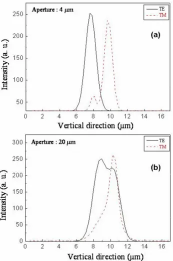
Figures 4(a) and 4(b) illustrate the near field profiles of the light at the MZ structure output for
both polarizations and for widths equal to 4 µm and 20 µm respectively. In Fig. 4(a) (solid line),
we see that, in the case of TE mode, the light is guided almost completely in the core layer which
has the lowest refractive index. On the other hand, for the TM mode (dashed line), the light is
propagated principally in the first cladding layer which has the highest refractive index and with
only a small amount of light propagated in the core layer. Furthermore, in Fig. 4(b), it can be
noticed that near field profiles present a very similar behavior but with less confinement of light
due to the increase of the width waveguide (20 µm). Therefore, the buried waveguides
FIG. 4. Experimental near-field profiles for both TE and TM polarizations at the MZ structure
output and for waveguide widths of 4 µm (a) and 20 µm (b).
We have also cleaved the MZ structure in the middle (Fig. 5(a)) in order to verify the
light propagation in the two arms. The near-field images measured and the 3D intensity profiles
for the width of 4 µm (Fig. 5(b) and 5(c)) at the output of each arm of the MZ structure are also
indicated. The intensity of the light is almost the same and the field distribution corresponds to a
waveguide constituting the MZ structure clearly presents, for the width of 4 µm, a shape that
allows good light confinement in the core layer both in the horizontal and vertical directions.
We have also verified the light propagation for the TM polarization which indicates the
same behavior as in the case of TE polarization but with a change in the output light intensity.
This demonstrates that we have developed a symmetrical MZ structure made with two similar
single mode buried ARROW for an aperture of 4 µm. This is an advantage for biosensing
applications since a good contrast of the interference fringes between the reference arm and the
sensing arm would be obtained.5
FIG. 5. Schematic of the cleaved MZ structure (a). Image of the near-field profiles at the output
of each arm of the cleaved MZ for a width of 4 µm (b) and corresponding 3D intensity profiles
(c). The input signal power was 3 mW.
Our interest in this work is to use the buried ARROW-MZ structure as an optical
transducer for biosensing applications by measuring the phase change between the reference arm
Since porous silicon material is strongly hydrophobic and unstable, a partial or total
oxidation of the porous structure is necessary, depending on the intended application such as
biosensing where a functionalization process is needed.27 Consequently, in order to use the MZ
structure based on porous silicon as a sensor, a second photolithography step to create the
aperture in the detection arm through which the molecules will be infiltrated, is required. This is
carried out after a heat treatment in wet oxygen. The sensor has been tested with ethanol to prove
the feasibility of this kind of MZ structure for sensing applications.
Figure 6 shows the evolution of the intensity, as measured by the photodiode, of the MZ
output signal versus time for an interaction length L = 5 mm. As soon as the ethanol is
introduced using a micro-syringe, we notice the appearance of interference fringes whose
amplitude varies significantly. Consequently, the uncertainty in the number of fringes recorded is
quite high due to optical losses and ethanol evaporation.28 By counting the number of fringes
(p = 16 ± 2) and considering complete ethanol evaporation, we deduce a refractive index
variation ∆n=2.48±0.3110−3 in the interaction area of the sensing arm using the following relationship: n p
L
λ
∆ = where 3 is the working wavelength (3 = 1.55 µm). This preliminary result is encouraging, but further study is needed to improve the performance of this
FIG. 6. Sensor response for a change of the refractive index in the detection arm using ethanol.
The design, fabrication and optical study of buried waveguide integrated in a MZ
structure based on porous silicon material have been presented. The theoretical study of
reflectance and BPM simulation allowed us to predict the propagated field along the propagation
direction in the structure, taking into account the experimental values of the refractive index and
of the thickness satisfying the antiresonant conditions for both polarizations. Optical near-field
measurements were carried out in order to check the light propagation behavior along the MZ
structure. The experimental results have indicated that for the TE mode, the optical propagated
field is located mainly in the core layer despite its low refractive index whereas for the TM
mode, the light is mostly guided in the first cladding layer. Therefore, both theoretical and
experimental studies, carried out without any post-treatment, demonstrate that the buried
waveguides constituting the MZ structure satisfy the antiresonant condition. These preliminary
studies have proved the feasibility of fabricating a MZ structure with buried ARROW based on
used for sensing applications. Our current work, in progress, is to test other biomolecules such as
BSA and HSA proteins using this integrated MZ structure.
Acknowledgments
This work is supported by the program PHC-Utique administered by the Joint Committee of
References
1
R. C. Alferness, IEEE J. Quantum Electron. 17, 946 (1981).
2
P.V. Lambeck, Sens. Actuators B. 8, 103 (1992).
3
R. Liu, T.A. Schmedake, Y.Y. Li, M.J. Sailor, Y. Fainman, Sens. Actuators B. 87, 58 (2002).
4
P.L. Edmiston, D.P. Campbell, D.S. Gottfried, J. Baughman, M. M. Timmers, Sens. Actuators B. 143, 574 (2010).
5
E. F. Schipper, A. M. Brugman, C. Dominguez, L. M Lechuga, R. P.H. Kooyman, and J. Greve, Sens. Actuators B. 40, 147 (1997).
6
R.G. Heideman 1, P.V. Lambeck, Sens. Actuators B. 61, 100 (1999).
7
F. Prieto, B. Sepulveda, A. Calle, A. Llobera, C. Dominguez, and L.M. Lechuga, Sens. Actuators B. 92, 151 (2003).
8
B. Maisenhölder, H. P. Zappe, R. E. Kunz, P. Riel, M. Moser, J. Edlinger, Sens. Actuators B. 38-39, 324 (1997).
9
P. Kozma, A. Hamori, S. Kurunczi, K. Cottier, R. Horvath, Sens. Actuators B. 155, 446 (2003).
10
B. Drapp , J. Piehler , A. Brecht, G. Gauglitz, B.J. Luff , J.S. Wilkinson and J. Ingenhoff, Sens. Actuators B. 38, 277 (1997).
11
D. Jimenez, E. Bartolome, M. Moreno, J. Munoz and C. Dominguez, Optics Communications 132, 437 (1996).
12
A. Halimaoui, Surface Science Letters. 306, 550 (1994).
13
R. Horvath, H. C. Pedersen and N. B. Larsen, Appl. Phys. Lett. 81, 2166 (2002).
14
R. Horvath, K. Cottier, H. C. Pedersen and J. J. Ramsden, Biosensors and Bioelectronics. 24, 799 (2008).
15
L. Haji, M. Hiraoui, N. Lorrain and M. Guendouz, Appl. Phys. Lett. 100, 111102 (2012).
16
M. Hiraoui, L. Haji, M. Guendouz, N. Lorrain, A. Moadhen and M. Oueslati, Biosensors and Bioelectronics 36, 212 (2012).
17
F. Prieto, L. M. Lechuga, A. Calle, A. Llobera, C. Dominguez, Journal of Lightwave Technology. 19, 75 (2001).
18
Shruti, R.K. Sinha, R. Bhattacharya, Opt. Quant. Electron. 41, 181 (2009).
19
20
V. P. Bondarenko, A. M. Dorofeev and N. M. Kazwchits, Microelectronic Engineering. 28, 447 (1995).
21
M. A. Duguay, Y. Kokubun and T.L. Koch, Appl. Phys. Lett. 49, 13 (1986).
22
D. E Aspnes, Thin Solid Films 89, 249 (1982).
23
M. Guendouz, P. Joubert and M. Sarret, Materials Science and Engineering B. 69, 43 (2000).
24
S. Nagata, S. Matsushita, K. Saito, Y. Ohshita, Y. Maeda, M. Yamaguchi and A. J. Ikushima, Appl. Phys. Lett. 82, 16 (2003).
25
M. Brinkmann, J. Hayden, M. Letz, Springer handbook of lasers and optics, ed. F. Trager New York (2007).
26
J. Yamauchi, J. Shibayama, O. Saito, O. Uchiyama and H. Nakano, J. Lightwave Technol. 14, 2401 (1996).
27
M.I. Baraton, W. Chang and B.H. Kear, J. Phys. Chem. 100, 16647 (1996).
28
List of figure Captions:
FIG. 1. Schematic and characteristic features of the MZ structure (a), SEM top view (b) and
cross section (c) micrographs of the buried waveguide which compose the MZ structure. The
width of the buried waveguide is 4 µm.
FIG. 2. Calculated reflectivity as a function of d1 for dc = 4.3 µm for both TE and TM
polarizations, with fixed experimental refractive index values nc = 1.65 ± 0.06, n1 = 2.95 ± 0.06,
n2 = 2.07 ± 0.06 and at working wavelength 3 = 1.55 µm.
FIG. 3. Cross section images and simulated near field profiles of the ARROW structure obtained
using the Beam Propagation Method (BPM) for TE (a, c) and TM (b, d) polarizations with the
following parameters: refractive index values nc = 1.65, n1 = 2.95, n2 = 2.07, a working
wavelength 3 = 1.55 µm, and thickness values dc = 4.3µm, d1 = 0.5 µm.
FIG. 4. Experimental near-field profiles for both TE and TM polarizations at the MZ structure
output and for waveguide widths of 4 µm (a) and 20 µm (b).
FIG. 5. Schematic of the cleaved MZ structure (a). Image of the near-field profiles at the output
of each arm of the realized cleaved MZ for a width of 4 µm (b) and corresponding 3D intensity
profiles (c). The power of the input signal is 3 mW.
FIG. 6. Sensor response for a change of the refractive index in the detection arm using ethanol