HAL Id: hal-01360411
https://hal.archives-ouvertes.fr/hal-01360411
Submitted on 13 May 2020
HAL is a multi-disciplinary open access
archive for the deposit and dissemination of
sci-entific research documents, whether they are
pub-lished or not. The documents may come from
teaching and research institutions in France or
abroad, or from public or private research centers.
L’archive ouverte pluridisciplinaire HAL, est
destinée au dépôt et à la diffusion de documents
scientifiques de niveau recherche, publiés ou non,
émanant des établissements d’enseignement et de
recherche français ou étrangers, des laboratoires
publics ou privés.
Low drive voltage electro-optic Bragg deflector using a
periodically poled lithium niobate planar waveguide
Imed Mhaouech, Virginie Coda, Germano Montemezzani, Mathieu Chauvet,
Laurent Guilbert
To cite this version:
Imed Mhaouech, Virginie Coda, Germano Montemezzani, Mathieu Chauvet, Laurent Guilbert. Low
drive voltage electro-optic Bragg deflector using a periodically poled lithium niobate planar
waveg-uide. Optics Letters, Optical Society of America - OSA Publishing, 2016, 41 (18), pp.4174-4177.
�10.1364/ol.41.004174�. �hal-01360411�
Low drive voltage electro-optic Bragg deflector using
periodically poled lithium niobate planar waveguide
I.
M
HAOUECH
1,2,*,
V.
C
ODA
1,2,
G.
M
ONTEMEZZANI
1,2,
M.
C
HAUVET
3,
L.
G
UILBERT
1,21
Université de Lorraine, LMOPS, EA 4423, 2 rue E. Belin, F-57070 Metz, France
2CentraleSupélec, LMOPS, EA 4423, 2 rue E. Belin, F-57070 Metz, France 3
FEMTO-ST Institute, UMR CNRS 6174, Université de Bourgogne Franche-Comté, 15B Avenue des Montboucons, F-25000 Besançon, France *Corresponding author: [email protected]
Received XX Month XXXX; revised XX Month, XXXX; accepted XX Month XXXX; posted XX Month XXXX (Doc. ID XXXXX); published XX Month XXXX
An electro-optic Bragg light deflector is demonstrated in a thinned periodically poled lithium niobate (PPLN) planar waveguide confined between two silica layers on a silicon substrate. More than 97% of diffraction efficiency is obtained with operating wavelength 633 nm for the two orthogonal light polarizations with a drive voltage of about 5 V. The temporal electric drift and the response time of the component are also studied. © 2016 Optical Society of America
OCIS codes: (230.2090) Electro-optical devices; (050.1950) Diffraction
gratings; (130.3730) Lithium niobate; (160.2100) Electro-optical materials; (130.4815) Optical switching devices; (230.7370) Waveguides
http://dx.doi.org/10.1364/OL.99.099999
Periodically poled ferroelectric crystals are currently used for frequency conversions using quasi-phase-matching [1], especially with Lithium Niobate (LN) thanks to its high nonlinear coefficients and mature poling process. LN is also a key material for electro-optic applications, especially for integrated modulators based on a Mach-Zehnder interferometer configuration using its large electrooptic (EO) coefficient [2]. Periodically poled lithium niobate (PPLN) can also be attractive also for EO applications. Several studies have been conducted on PPLN-based EO deflectors in the visible range [3,4], near infrared [5] or UV range [6] in Bragg configuration and more recently in Raman-Nath configurations [7,8]. First attempts have been carried out using standard 500-µm-thick LN wafers, requiring drive voltages of hundreds of volts [3– 5]. Recently PPLN has been thinned to lower the required applied voltage [6,8]. Okazaki et al. polished the crystal up to a thickness of 35 μm achieving a planar waveguide configuration and a drive voltage of 90 V [8]. For practical EO applications in integrated devices, drive voltages as low as 5 V are usually required. This goal
has been approached in a periodically-poled LiTaO3 waveguide
using a voltage of 10 V for the demonstration of a spatial light modulator based on an electro-optic Bragg grating [9]. In this letter we use a recent technique to realize high-quality isolated crystalline film out of LN [10,11] to implement an electro-optic Bragg deflector with a drive voltage below 10 V. We accomplish an
efficient spatial light deflector either for an extraordinary or an ordinary light polarization.
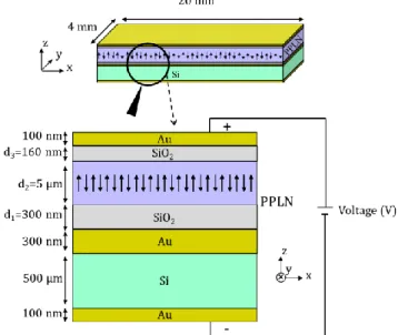
Figure 1 shows schematically our PPLN waveguide sandwiched between two electrodes. The first step of the component fabrication is the periodic poling of a 500-μm thick commercial Z-cut congruent LN wafer, by application of an intense electric field at room temperature. A standard period Λ of 18.6 µm is chosen for
the periodic poling. In a second step, a silica (SiO2) layer (of
thickness d1 = 300 nm) is deposited by inductively-coupled plasma
enhanced chemical vapor deposition (ICPECVD) onto one face of the poled wafer followed by the sputtering of a gold layer. A 500-μm thick silicon wafer is also coated with a gold layer. The metalized faces of both the PPLN and silicon wafers are then placed into contact and pressed in a wafer bonding machine leading to a 300-nm thick gold interlayer. The bonding process is realized at room temperature, which prevents mechanical stress that could occur due to the dissimilar temperature coefficients of the two wafers. The LN layer is then mechanically ground and
polished with a silica abrasive to get a LN film with a thickness of d2
= 5 μm. This gives a mode size close to 4 µm at 1/e2. This hybrid
wafer is then diced and polished at the same time using a precision diamond saw to form a 20-mm (x-axis) by 5-mm (y-axis) rectangular sample. The 5-mm width of the sample is parallel to the ferroelectric domain walls but the poling is effective only over 4 mm. The poling is homogeneous over this length and it forms a
short device. A second SiO2 layer of thickness d3 = 160 nm is
deposited on the top surface of the PPLN crystal by RF sputtering. Finally two 100-nm gold layers are deposited by evaporation on
the upper SiO2 layer and on the bottom silicon substrate surfaces.
These two gold layers allow the application of a uniform electric field to activate the electro-optic effect. The silica layers on both sides of the PPLN film form a dielectric step-index planar optical waveguide thanks to the index difference between silica
(𝑛𝑆𝑖𝑂2= 1.45 ) and LN (𝑛𝐿𝑁≈ 2.2). Silica thicknesses are kept
low to minimize the voltage drop in the silica layers. A propagation loss of 0.8dB/cm has been measured in ridge waveguides with a similar architecture [20], loss is assumed to be lower for the present planar structure.
FIG. 1. Illustration of the different layers constituting the realized electro-optic Bragg deflector based on a periodically poled lithium niobate in a planar waveguide configuration.
The PPLN waveguide structure described in the previous section has been developed to be used as a spatial light deflector with two output ports driven by the electro-optic effect. If no voltage is applied to the PPLN, a light beam launched at Bragg angle in the waveguide should not be deviated. When a drive voltage is applied between the electrodes, this beam is diffracted by the refractive index grating induced by the EO effect. Throughout this letter, since the electric field E is parallel to the polar axis (z) and the light polarization is either ordinary (o) or extraordinary (e), the index grating amplitude is given by [5]:
E r n n E r n no o e e 33 3 13 3 2 1 , 2 1 . (1)
(Depending on the light polarization). ne is the extraordinary
refractive index and no is the ordinary refractive indexof LN. The
EO coefficient is r33 for an extraordinary polarization and r13 for an
ordinary polarization. At 633 nm, ne= 2.203, no = 2.286 [12], r13 =
9.6 pm/V and r33 = 30.9 pm/V [13]. E is the electric field in the
PPLN layer. The experimental configuration for the optical characterization is schematically represented in Fig. 2. We use a He-Ne laser (633 nm), a polarizer and a telescope combined with a cylindrical lens to shape a beam of elliptical section. The sample is mounted on a 5-axis sample holder to optimize the light coupling to the fundamental mode of the planar waveguide and to adjust the propagation direction to an angle α between the wave vector and the y-axis of the crystal to the Bragg condition. The external
angle ensuring Bragg condition is given by sin 𝛼 = 𝜆/2Λ = 0.97°.
The transmitted and diffracted beams are separately monitored by two photodiodes plugged to a digital storage oscilloscope to
measure their transmitted (It) and diffracted (Id) power. The
diffraction efficiency of the Bragg deflector is measured as
𝜂𝑒𝑥𝑝= 𝐼𝑑⁄(𝐼𝑑+ 𝐼𝑡).
FIG. 2. Configuration of the waveguide electro-optic Bragg deflector tested both with ordinary and extraordinary light polarizations.
In the Bragg regime, the diffraction efficiency ηth is theoretically
given by [14]: ) cos( sin2 Bi i i th L n . (2)
The subscript i refers to the light polarization (i = o, e). In eq. (3), L = 4 mm is the length of the PPLN waveguide where the EO effect is
activated, Bi (ϴBe= 0.44°, ϴBo= 0.43°) is the internal Bragg angle
It’s important to note that the calculation of ηth by Eqs. (1) and (2)
takes into account the multi-layer dielectric structure of our component. The silicon substrate is considered as a perfect conductor due to its large conductivity compare to silica and LN. When the voltage U is switched on at t = 0, the electric field present in the LN layer can be deduced from the continuity condition of the electric displacement field. The electric field E in the PPLN layer is thus given by:
2 3 1 2 ( ) / 2 d U d d d U E SiO LN (3)
with di the thicknesses of the respective layers (as illustrated on
Fig. 1) and i the low-frequency dielectric permitivities: 𝜀𝑆𝑖𝑂2= 3.9
[15] and 𝜀𝐿𝑁= 35 along the polar axis [16]. The presence of the
low permittivity silica layers gives an effective voltage applied on the LN layer reduced by a factor δ ≈ 2 compare to the applied voltage U.
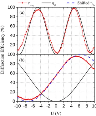
Fig. 3(a) displays ηexp and ηth versus the applied voltage U for an
extraordinary polarization. We can see that the 3-dielectric-layer model (Fig. 3(a) continuous line) is in very good agreement with the experiment (Fig. 3(a) connected squares). A very good efficiency with a maximum at 98% is notably achieved for an applied voltage U = 4.6 V for the e-polarization. The periodicity of the response is also well described. Consequently, a very good agreement between the experimental measurements and the theoretical predictions is obtained for e-polarization without any free parameter for the modeling.
However, for the o-polarization, while the experimental (Fig. 3(b), red squares) maximum diffraction (97%) and period is once again in accordance with the theoretical curve (solid line), the theoretical curve must be arbitrary shifted by -7.5 V (dotted line) to take into account the high diffraction efficiency (~50%) already measured at 0 V. We note that this shift gives diffraction efficiency close to 100% independently of the polarization with U = 5 V. It is important to note that the amplitude of the applied voltage must
be kept low to stay in the Bragg regime. High voltage can indeed make the Raman-Nath regime to appear [17].
20 40 60 80 100 -10 -8 -6 -4 -2 0 2 4 6 8 10 0 20 40 60 80 100 (b) (a) exp th Shifted th U (V) Diffr ac ti on E ffi ci en cy (%)
FIG. 3. Diffraction efficiency versus applied voltage U for (a) e-polarized light and (b) o-polarized light. Red points are experimental data. Black solid lines are theoretical curves according to eq. (3). The blue dash line in Fig. 3(b) is shifted from the latter by an offset Uo = -7.5 V.
Previous publications dealing with EO functionalities in PPLN have already depicted similar effects on both polarizations which is attributed to the presence of a permanent refractive index due to
an internal field Ei created by the poling process [4–6]. These
works reported Ei on the order of 106 V/m [18,19]. The shift of
𝑈𝑜= −7.5 𝑉 observed for the o-polarization could correspond
to a field Ei = 3.5 106 V/m. However, such an Ei should induce an
offset of +3.3 V for the e-polarization response. This positive shift is a consequence of the periodicity of the diffraction efficiency. This value doesn't correspond to the one we observe experimentally (Ue = +0.2 V). Therefore we cannot ascribe the observed shift
solely to an internal field.
The offsets are probably also related to our specific thinning process using chemico-mechanical polishing. Since –Z and +Z faces are etched at slightly different speeds, a periodic corrugation is present at the surface of the PPLN and forms a permanent surface grating. The amplitude of the corrugation measured with an optical profilometer is 40 nm [20], the less thinned parts corresponding to +Z domains. This amplitude is large enough to constitute a surface Bragg grating with the very same periodic that the voltage controlled grating. Since +Z oriented regions of the PPLN are thicker than –Z oriented regions, we can conclude that the surface grating is in phase with a EO grating induced with a positive applied voltage U. This is consistent with the increase of the diffraction efficiency obtained when a weak positive voltage is applied. Moreover, a qualitative analysis based on coupled mode theory shows that the corrugation grating gives a coupling coefficient between the transmitted and the diffracted beams for
the o-polarization six times larger than for a e-polarization [21]. It is therefore in accordance with the experimental observations that reveals a larger diffraction for the o-polarization than the e-polarization in the absence of applied voltage. Nevertheless, it is unlikely to explain both offsets only with the effect the corrugated grating. So we believe that both, the effects of the corrugation grating and of the presence of an internal field are required to explain the experimental offsets observed on Fig. 3. Moreover, thanks to these effects, the maximum diffraction efficiency is achieved for both polarizations with a similar applied voltage of about 5 V, even if the switching voltage is about 12V for o-polarization in accordance with the EO coefficients ratio.
Note that the dielectric regime given by Eq. (3) is valid immediately after the application of a bias but the ohmic regime has to be taken into account at longer time. For a very long exposure time to the applied voltage (𝑡 → ∞), by virtue of the current continuity, we found that the electric field should be
entirely confined in the LN layer and should therefore tend to U/d2
(𝛿 → 1), providing that the LN electrical conductivity 𝜎𝐿𝑁 is much
lower than the silica one (𝜎𝑆𝑖𝑂2). Between these two extreme
values E(0) and E(), the electric field E(t) is expected to exhibit a
first-order transient regime, with a time constant approximately
equal to the Maxwell time constant = 0𝑆𝑖𝑂2/𝜎𝑆𝑖𝑂2, where 0 is
the vacuum permittivity. A similar behavior is thus expected for the diffraction efficiency if we consider a linear part of the diffraction efficiency versus voltage response. This so-called drift phenomenon is known as a severe issue, affecting the stability of LN-based EO modulators elsewhere reported in [22].
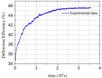
It has been experimentally studied in our Bragg deflector. The results presented in Fig. 4 shows the time variation of the experimental diffraction efficiency as a function of time. The applied voltage is set to 2 V in order to remain in the linear part of
the curve of Fig. 3(a). Like in Fig. (3), at t = 0, ηexp(0) = 34%. As
expected, ηexp increases exponentially with a time constant τ ≈ 640
s, before it stabilizes to 45.5%. After a long exposure, if all the
applied electric field were confined in the PPLN, ηexp should reach
about 90%. However, ηexp stabilizes at a much lower value, as
depicted on Fig.(4). Non-ohmic contacts between layers could be the reason. This can also suggests that the conductivities of LN and
SiO2 in our component are not extremely different. For LN of
optical quality, bulk conductivity values ranging from 10-16 to 10-18
-1cm-1 [23], whereas for silica layers they range typically from 10
-12 to 10-16-1cm-1 [24], depending on the deposition technique and
conditions. From our measurements, we may infer that the conductivity of the silica layers of our component is rather low,
~510-16-1cm-1, as deduced from the time constant = 640 s. We
checked experimentally than this troublesome drift phenomenon is nevertheless absent by working our deflector with an AC voltage around a 0-V DC value.
This AC regime was used to characterize the dynamic response of the structure as a function of frequency. As for the experiment reported in Fig. (4), the operating point is set in the linear part of the diffraction efficiency curve with an AC voltage of a peak to peak amplitude equal to 1.5 V and an offset of 2 V. The cutoff frequency
is fexp= 5.7 kHz. The theoretical analysis of the multilayer structures
modeled by an equivalent electric system gives a cutoff frequency
several orders of magnitude higher than fexp. This low cutoff
frequency is due to the oxidized surfaces of the silicon wafer, which creates a parasitic resistance in the circuit. Higher cutoff frequencies can be achieved by applying the electrical signal
between the upper electrode and the bonding gold layer. Such an arrangement tested on dummy samples gives a cutoff frequency in better accordance with the theoretical predictions. Reduction of the component footprint should thus allow modulation frequencies of several MHz. 0 1 2 3 4 34 36 38 40 42 44 46 Experimental data Diff raction Efficiency (%) time (103s)
FIG. 4. Experimental time evolution of the diffraction efficiency highlighting the electric drift time of the E0 Bragg modulator.
In conclusion, thanks to the original fabrication of a PPLN planar waveguide using a precise polishing to thin the LN wafer down to 5 µm, an efficient electro-optic Bragg deflector has been realized. This component works at a very low drive voltage (around 5 V) with a very good efficiency (more than 97%). The time electric drift and the response time of the component under an AC voltage were also investigated. This demonstration of an EO-PPLN component with such a manufacturing process opens the way to more complex devices and further improvements. Firstly, the cutoff frequency should be increased by improving the electrode quality. A better optimization of the silicon substrate and of the dielectric layers on each side of the PPLN should also reduce the response time. The additional Bragg diffraction due to the surface grating on the top of the PPLN can be suppressed. To do that, an alternative thinning process using a precision saw [20] will replace the thinning by polishing. Therefore promising alternative EO-PPLN components in a waveguide configuration, such as an integrated active Bragg mirror working at telecommunications wavelengths, should be further developed.
Acknowledgment. The authors are grateful to the Region Lorraine for financial support of this research work, to FEMTO ENGINEERING for its contribution to the realization of the modulator.
References
1. D. A. Scrymgeour, in Ferroelectric Crystals for Photonic Applications, P. Ferraro, S. Grilli, and P. D. Natale, eds., Springer Series in Materials Science No. 91 (Springer Berlin Heidelberg, 2014), pp. 385–399. 2. E. L. Wooten, K. M. Kissa, A. Yi-Yan, E. J. Murphy, D. A. Lafaw, P. F.
Hallemeier, D. Maack, D. V. Attanasio, D. J. Fritz, G. J. McBrien, and D. E. Bossi, IEEE J. Sel. Top. Quantum Electron. 6, 69–82 (2000).
3. H. Gnewuch, C. N. Pannell, G. W. Ross, P. Smith, and H. Geiger, IEEE Photonics Technol. Lett. 10, 1730–1732 (1998).
4. M. Yamada, Rev. Sci. Instrum. 71, 4010–4016 (2000).
5. J. A. Abernethy, C. B. E. Gawith, R. W. Eason, and P. G. R. Smith, Appl. Phys. Lett. 81, 2514–2516 (2002).
6. T. Inoue and T. Suhara, IEEE Photonics Technol. Lett. 23, 1252–1254 (2011).
7. M. Okazaki and T. Suhara, IEEE Photonics Technol. Lett. 26, 2334–2336 (2014).
8. M. Okazaki and T. Suhara, J. Light. Technol. 33, 5195–5200 (2015). 9. M. Okazaki, S. Yoshimoto, T. Chichibu, and T. Suhara, IEEE Photonics
Technol. Lett. 27, 1646–1648 (2015).
10. M. Chauvet, F. Bassignot, F. Henrot, F. Devaux, L. Gauthier-Manuel, H. Maillotte, G. Ulliac, and B. Sylvain, Opt. Lett. 40, 1258 (2015). 11. M. Chauvet, F. Henrot, L. Gauthier-Manuel, F. Devaux, V. Pêcheur, and
H. Maillotte, Proc. SPIE 9891, (2016).
12. D. S. Smith, H. D. Riccius, and R. P. Edwin, Opt. Commun. 17, 332–335 (1976).
13. K. F. Hulme, P. H. Davies, and V. M. Cound, J. Phys. C Solid State Phys. 2, 855 (1969).
14. H. Kogelnik, Bell Syst. Tech. J. 48, 2909–2947 (1969).
15. F. Giustino, P. Umari, and A. Pasquarello, Microelectron. Eng. 72, 299– 303 (2004).
16. M. Abarkan, M. Aillerie, J. P. Salvestrini, M. D. Fontana, and E. P. Kokanyan, Appl. Phys. B 92, 603–608 (2008).
17. M. G. Moharam, T. K. Gaylord, and R. Magnusson, Opt. Commun. 32, 19–23 (1980).
18. V. Gopalan, T. E. Mitchell, Y. Furukawa, and K. Kitamura, Appl. Phys. Lett. 72, 1981–1983 (1998).
19. L. Guilbert, Opt. Express. 17, 10782–10785 (2009).
20. M. Chauvet, F. Henrot, F. Bassignot, F. Devaux, L. Gauthier-Manuel, Vincent Pêcheur, H. Maillotte, and B. Dahmani, J. Opt. 18, 85503 (2016).
21. H. Nishihara, M. Haruna, and T. Suhara, in Optical Integrated Circuits, R. E. Fischer and W. J. Smith, eds., McGraw-Hill Optical and Electro-optical Engineering Series (McGraw-Hill, New York, 1989), Chap. 4, pp. 62–95. 22. J. P. Salvestrini, L. Guilbert, M. Fontana, M. Abarkan, and S. Gille, J.
Light. Technol. 29, 1522–1534 (2011).
23. T. Volk and M. Wöhlecke, Lithium Niobate: Defects, Photorefraction and Ferroelectric Switching (Springer Science & Business Media, 2008). 24. C. Raynaud, J. Non-Cryst. Solids 280, 1–31 (2001).