T
T
H
H
È
È
S
S
E
E
En vue de l'obtention du
D
D
O
O
C
C
T
T
O
O
R
R
A
A
T
T
D
D
E
E
L
L
’
’
U
U
N
N
I
I
V
V
E
E
R
R
S
S
I
I
T
T
É
É
D
D
E
E
T
T
O
O
U
U
L
L
O
O
U
U
S
S
E
E
Délivré par l’Université Toulouse III – Paul Sabatier en cotutelle avec l’Université Autonome de Barcelone
Mention Européenne
Discipline ou spécialité: Nanophysique
JURY
Luis A. Morellón Alquézar Président du jury Jaume Gázquez Alabart Secrétaire Francesca Peiró Martínez Rapporteur Yves Dumont Rapporteur Michel Goiran Examinateur Guillaume Saint-Girons Examinateur Bénédicte Warot-Fonrose Directeur de thèse Florencio Sánchez Barrera Directeur de thèse
Nom Nom Nom
... (préciser la qualité de chacun des membres)
Ecole doctorale: Science de la Matière (EDSDM)
Unité de recherche: Centre d’élaboration de matériaux et d’études structurales (CEMES) & Instituto de Ciencia de Materiales de Barcelona (ICMAB)
Directeurs de Thèse: Bénédicte Warot-Fonrose (CNRS) et Florencio Sánchez (CSIC)
Présentée et soutenue par Patricia de Coux González Le 30 Septembre 2013
Title: “Integration of ferrimagnetic CoFe2O4 epitaxial films with silicon”
Integration of ferrimagnetic CoFe
2O
4epitaxial films with silicon
Patricia de Coux González
PhD Thesis
Supervisors: Dr. Bénédicte Warot-Fonrose Dr. Florencio Sánchez Barrera
Members of the jury:
Luis A. Morellón Alquézar Jaume Gázquez Alabart Francesca Peiró Martínez Yves Dumont Michel Goiran
Guillaume Saint-Girons Bénédicte Warot-Fonrose Florencio Sánchez Barrera
President du jury Secrétaire Rapporteur Rapporteur Examinateur Examinateur Directeur de Thèse Directeur de Thèse
Ecole doctorale science de la matière (EDSDM)
Manuscrit présenté pour l’obtention du titre de Docteur avec Mention Européenne Barcelona, 30 September 2013
i
Abstract
Microelectronics is progressing continuously by the exponential growth with time of the number of transistors per integrated circuit, the popularly known as “Moore’s Law”. This law is still valid but it is approaching intrinsic limits. The “More than Moore” is a complementary approach based on the use of radically new concepts as well as on the use of new materials in existing devices to improve performance. In particular, functional complex oxides represent an opportunity to extend and develop new devices functionalities with a wide range of applications.
This thesis presents a study on the integration of CoFe2O4 thin films with silicon. CoFe2O4 is ferromagnetic and electrically insulating at room temperature, the properties required to be used as tunnel barrier in a spin filter device. This device could permit the injection of spin polarized currents in silicon, as an alternative to the injection using ferromagnetic electrodes and passive tunnel barriers. However the spin filter requires a nanometric CoFe2O4 film, thinner than 4-5 nm to allow tunneling, and has to be epitaxial with high crystalline quality to preserve the ferromagnetism and tunneling transport. The thermodynamical instability between CoFe2O4 and silicon imposes the use of a buffer layer for its epitaxial integration. The challenging goal is therefore fabricating ultrathin epitaxial CoFe2O4/buffer bilayers on silicon. Investigating the possibility to achieve such goal has been the main objective of this thesis.
The buffer layer is critical. Thus we have followed a strategy based on investigating in parallel several candidates. SrTiO3, which can be grown epitaxially on Si(001) with sharp interface and that has been already used as single crystal to deposited CoFe2O4, has been a natural option. We have used thick (around 17 nm) SrTiO3 buffers fabricated by collaborators at INL-Lyon to grow by pulsed laser deposition (PLD) CoFe2O4, which is epitaxial and ferromagnetic. However, there is diffusion of Ti into CoFe2O4 and the SrTiO3/Si(001) interface could be unstable.
Yttria-stabilized-zirconia (YSZ) has been other investigated material. It is widely used to grow oxides on Si(001), but having the YSZ buffers high thickness of tens of nm and presence of interfacial SiOx. Here we have investigated the mechanisms of YSZ epitaxy to determine the limits reducing the YSZ thickness and the interfacial layer. Ultrathin buffers around 2 nm thick, with less than 1 nm thick SiOx layer, can be fabricated by reflection high energy electron diffraction (RHEED) assisted PLD. Ultrathin CoFe2O4 films subsequently
ii
grown were epitaxial, although (111) oriented and with the SiOx layers more than 2 nm thick. The result is remarkable, but the total thickness of CFO/YSZ/SiOx is excessive for a tunnel device.
We have used also Sc2O3 and Y2O3 buffers on Si(111), provided by collaborators at IHP-Frankfurt Oder. They are original candidates never combined with CoFe2O4. In spite of the huge lattice mismatch of around 15 and 20% CoFe2O4 grows epitaxially. Detailed transmission electron microscopy (TEM) has showed a mechanism of domain matching epitaxy. The films present magnetization close to the bulk value and without interfacial SiOx layer in the CoFe2O4/Y2O3/Si(111) sample. Thus Y2O3 appear as very promising buffer layer and maybe convenient for the nanometric structure required in a spin filter. We have demonstrated that ultrathin Y2O3 buffers, less than 2 nm thick, permit epitaxial growth of CoFe2O4, although the investigation of the interface stability has not been conclusive.
iii
Résumé
Le progrès continu en microélectronique est dû à la croissance exponentielle avec le temps du nombre de transistors par circuit intégré, relation connue comme la loi de Moore. Cette loi reste vraie, mais approche ses limites intrinsèques. C’est pourquoi est apparue la loi de “More than Moore” qui est une approche complémentaire basée sur de nouveaux concepts et l’introduction de nouveaux matériaux pour améliorer les performances dans les dispositifs actuels. En particulier, les oxydes fonctionnels représentent une bonne opportunité pour accroître et développer les réponses des dispositifs d’intérêt pour une large gamme d’applications.
Cette thèse présente une étude sur l’intégration de couches minces de CoFe2O4 sur silicium. CoFe2O4 est ferromagnétique et isolant électrique à température ambiante, qui sont les propriétés requises pour être utilisé en tant que barrière tunnel dans un dispositif de filtre à spin. Ce dispositif pourrait permettre l’injection de courants de spin polarisés dans le silicium, comme alternative à l’injection utilisant des électrodes ferromagnétiques et des barrières tunnel passives. Cependant, un filtre à spin nécessite une couche mince de CoFe2O4 avec une épaisseur nanométrique, inférieure à 4-5 nm pour permettre l’effet tunnel, et une épitaxie de très bonne qualité afin de préserver le ferromagnétisme et le transport par effet tunnel. L’instabilité thermodynamique entre CoFe2O4 et le silicium impose l’utilisation d’une couche tampon pour son intégration épitaxiale. L’exigeant défi est donc de fabriquer des bicouches épitaxiées et ultrafines de CoFe2O4/couche tampon sur silicium. Le principal objectif de cette thèse a été d’étudier la possibilité d’accomplir cet objectif.
La couche tampon est essentielle. Nous avons donc adopté une stratégie de recherche en parallèle considérant différents candidats. SrTiO3, pouvant croître épitaxié sur Si(001) avec une interface nette et ayant déjà été utilisé sous forme de substrat monocristallin pour déposer CoFe2O4, a été une option naturelle. Nous avons utilisé des couches tampon de SrTiO3 épaisses (environ 17 nm) fabriquées par des collaborateurs de l’INL-Lyon pour déposer des couches de CoFe2O4 épitaxiées et ferromagnétiques par dépôt par laser pulsé (pulsed laser
deposition, PLD). Nous avons décelé une diffusion de Ti dans CoFe2O4, et une possible instabilité de l’interface SrTiO3/Si(001).
L’Yttrium stabilisé avec de la zircone (yttria-stabilized zirconia, YSZ) est un autre oxyde largement utilisé comme couche tampon pour intégrer des oxydes sur Si(001). Cependant, il est utilisé avec des épaisseurs de dizaines de nanomètres et présentant une
iv
couche interfaciale de SiOx. C’est pourquoi nous avons étudié les mécanismes de croissance épitaxiale d’YSZ afin de déterminer les limites de réduction d’épaisseur d’YSZ et de la couche interfaciale. Nous avons obtenu des couches ultrafines de buffer d’environ 2 nm d’épaisseur avec moins d’1 nm de SiOx par PLD monitorisé par RHEED (reflection high
energy electron diffraction). En utilisant ces couches tampon, les couches ultrafines de
CoFe2O4 épitaxiées présentent une orientation (111) et des couches interfaciales de SiOx supérieures à 2 nm d’épaisseur. Bien que le résultat soit remarquable, l’épaisseur totale de CFO/YSZ/SiOx est excessive pour un dispositif de filtre à spin.
Nous avons aussi utilisé des buffers de Sc2O3 et Y2O3 sur Si(111), fournis par des collaborateurs de l’IHP-Frankfurt Oder. Ce sont des candidats originaux qui n’ont jamais été combinés avec CoFe2O4. En dépit de leur grand désaccord paramétrique avec CoFe2O4, entre 15 et 20%, la croissance de CoFe2O4 est épitaxiale. La caractérisation par microscopie électronique en transmission a montré le mécanisme de croissance épitaxiale par domaines. Les films présentent une magnétisation proche de celle du matériau massif et sans couche interfaciale de SiOx dans des hétérostructures des échantillons de CoFe2O4/Y2O3/Si(111). Les buffers d’Y2O3 sont donc très prometteurs pour la structure nanométrique requise dans un filtre à spin. Nous avons démontré que des buffers ultrafins d’Y2O3, avec une épaisseur inférieure à 2 nm, permettent la croissance épitaxiale de CoFe2O4, même si les recherches sur la stabilité de l’interface n’ont pas été concluantes.
v
Resumen
El continuo progreso en microelectrónica se debe al crecimiento exponencial con el tiempo del número de transistores por circuito integrado, dependencia conocida como ley de Moore. Esta ley se sigue cumpliendo, pero se va acercando a límites intrínsecos. Por ello ha emergido la alternativa “More tan Moore”, un enfoque complementario basado en conceptos radicalmente nuevos y en la introducción de nuevos materiales que mejoren las prestaciones de dispositivos. En particular, los óxidos funcionales representan una buena oportunidad para incrementar y desarrollar las respuestas de dispositivos de interés para una gran gama de aplicaciones.
Esta tesis presenta un estudio sobre la integración de capas delgadas de CoFe2O4 sobre silicio. CoFe2O4 es ferromagnético y un aislante eléctrico a temperatura ambiente, que son las propiedades requeridas para ser utilizado como barrera túnel en un dispositivo de filtro de espín. Dicho dispositivo podría permitir la inyección de corrientes de espines polarizados en silicio, como alternativa a la inyección usando electrodos ferromagnéticos y barreras túneles pasivas. Sin obstante, un filtro de espín necesita una capa fina de CoFe2O4 de espesor nanométrico, inferior a 4-5 nm para permitir el efecto túnel, y una epitaxia de muy buena calidad para conservar el ferromagnetismo y el transporte por efecto túnel. La instabilidad termodinámica de CoFe2O4 con el silicio impone el uso de una capa barrera para su integración epitaxial. El mayor desafío reside en fabricar bicapas epitaxiales y extrafinas de CoFe2O4/barrera sobre silicio. El principal objetivo de esta tesis ha sido estudiar la posibilidad de realizar este objetivo.
La capa barrera es crucial. Hemos llevado a cabo una estrategia de investigación en paralelo considerando varios candidatos. SrTiO3, pudiendo crecer de forma epitaxial sobre Si(001) y ya usado como substrato monocristalino para el depósito de CoFe2O4, ha sido una opción evidente. Hemos usado capas búfer de SrTiO3 gruesas (alrededor de 17 nm) fabricadas por colaboradores del INL-Lyon para crecer capas de CoFe2O4 epitaxiales y ferromagnéticas mediante depósito con láser pulsado (pulsed laser deposition, PLD). Sin embargo hemos encontrado difusión de titanio en el CoFe2O4, y que la intercara de SrTiO3/Si(001) podría ser inestable.
Zirconia estabilizada con ítria (yttria-stabilized zirconia, YSZ) es otro óxido ampliamente usado como lámina barrera para la integración de óxidos sobre Si(001). Sin
vi
embargo siempre se usa siendo una barrera gruesa, con espesores de decenas de nanómetros y presentando una capa de SiOx en la intercara. Por ello hemos invesigado los mecanismos de crecimiento epitaxial de YSZ, con el fin de determinar los límites en la reducción de espesor de YSZ y de SiOx. Como resultado podemos obtener láminas barrera ultrafinas, de aproximadamente 2 nm de espesor y con menos de 1 nm de SiOx Ha sido posible usando PLD monitorizado con RHEED (reflection high energy electron diffraction). Usando estas láminas barrera, capas ultrafinas de CoFe2O4 epitaxiales presentan una orientación (111) y capas interfaciales de SiOx superiores a 2 nm de espesor. Aunque el resultado es remarcable, el espesor total de CFO/YSZ/SiOx es excesivo para un dispositivo de filtro de espín.
También hemos utilizado barreras de Sc2O3 y Y2O3 sobre Si(111), proporcionadas por colaboradores del IHP-Frankfurt Oder. Son candidatos originales que no se habían combinado nunca con CoFe2O4. A pesar del gran desajuste estructural con el CoFe2O4, de entre 15 y 20%, el crecimiento de CoFe2O4 es epitaxial. La caracterización por microscopia electrónica en transmisión ha mostrado un mecanismo de crecimiento epitaxial por ajuste dominios. Las capas presentan una magnetización cercana a la del material masivo y sin capa interfacial de SiOx en las heteroestructuras de CoFe2O4/Y2O3/Si(111). Las barreras de Y2O3 son por tanto prometedoras para la estructura nanométrica requerida en un filtro de espín. Hemos demostrado que barreras ultrafinas de Y2O3, con un espesor inferior a 2 nm, permiten el crecimiento epitaxial de CoFe2O4, aunque las investigaciones sobre la estabilidad de la intercara no han sido concluyentes.
vii
Table of contents
Chapter I: General introduction ... 1
I.1 Context and objectives ... 1
I.1.1 Complex oxides ... 1
I.1.2 Multiferroics and magnetoelectric oxides: a paradigm of functional oxides ... 3
I.1.3 Integration of functional oxides on silicon ... 4
I.1.4 Objectives of the thesis ... 5
I.2 CoFe2O3 ... 5
I.3 Oxides on silicon ... 7
I.3.1 Metal oxide/Silicon interface: thermodynamics ... 8
I.3.2 Incompatibility of CoFe2O4 with silicon ... 9
I.4 Outline of the thesis ... 10
Chapter II: Experimental techniques ... 11
II.1 Elaboration techniques ... 11
II.1.1 Molecular Beam Epitaxy (MBE) ... 11
II.1.2 Pulsed Laser Deposition (PLD) ... 11
II.2 Diffraction techniques ... 13
II.2.1 Theory of diffraction ... 14
II.2.2 X-Ray diffraction ... 15
II.2.3 Electron diffraction ... 16
II.2.3.1 Reflection High-Energy Electron Diffraction (RHEED) ... 16
II.2.3.2 Transmission electron diffraction by TEM ... 17
II.3 Transmission Electron Microscopy (TEM) ... 19
II.3.1 Interface contrast ... 21
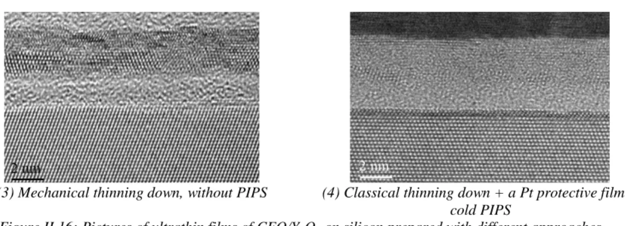
II.3.2 TEM sample preparation methods ... 21
II.3.3 Particular TEM sample preparations ... 26
II.3.3.1 TEM sample preparation for the oxide/silicon interface characterization ... 26
II.3.3.2 Improving TEM preparation for ultrathin oxide films integrated on silicon .... 27
Chapter III: Integration of CoFe2O4 with Si(001) using SrTiO3 buffer layers ... 31
III.1 Introduction ... 31
III.2 SrTiO3 on Si(001) ... 32
III.3 CoFe2O4 on Si(001) buffered with SrTiO3 ... 35
III.3.1. In-situ RHEED, AFM and XRD characterization ... 35
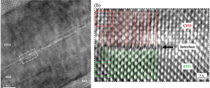
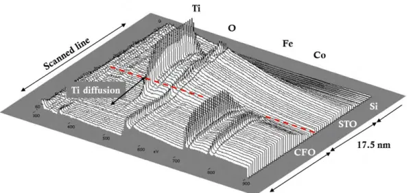
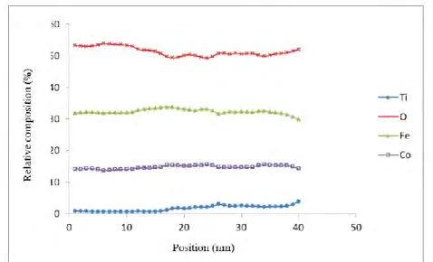
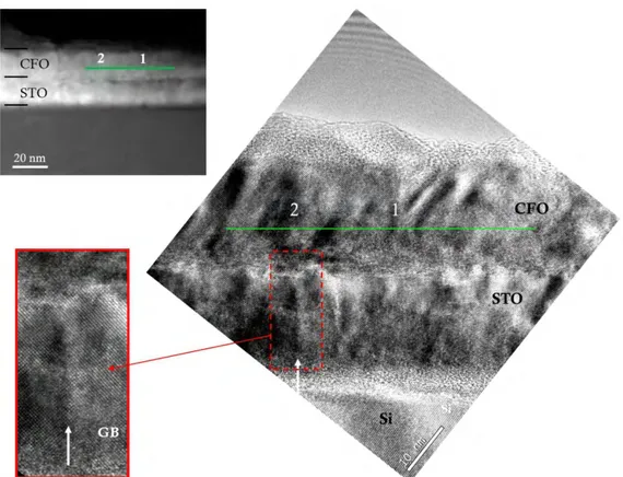
III.3.2 Structural characterization by TEM ... 36
III.3.3 EELS characterization ... 40
III.3.3.1 EELS in a direction perpendicular to the interface ... 40
III.3.3.2 EELS along a direction parallel to the interface ... 43
viii
Chapter IV: Integration of CoFe2O4 with Si(001) using YSZ buffer layers ... 49
IV.1 Introduction ... 49
IV.2 CoFe2O4 on Si(001) using CeO2/YSZ double buffers ... 50
IV.3 Growth mechanisms of yttria stabilized zirconia on Si(001) ... 52
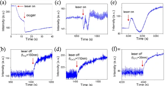
IV.4 Integration of ultrathin CoFe2O4/YSZ with Si(001) ... 59
IV.5 Summary ... 62
Chapter V: Integration of CoFe2O4 with Si(111) using A2O3 (A=Sc, Y) buffer layers .. 65
V.1 Introduction ... 65
V.1.1 Materials ... 66
V.1.2 Domain Matching Epitaxy ... 67
V.1.2.1 Description of the mechanism ... 67
V.1.2.2 CoFe2O4 on A2O3: possibilities of domain matching epitaxy ... 69
V.2 CoFe2O4 on Sc2O3 buffered Si(111) ... 70
V.2.1 Introduction ... 70
V.2.2 Thin film growth and in-situ characterization by RHEED ... 71
V.2.3 AFM and XRD of CoFe2O4 and Sc2O3 films on Si(111) ... 72
V.2.4 HRTEM characterization ... 73
V.2.5 Magnetic properties ... 76
V.3 CoFe2O4 on Y2O3 buffered Si(001) ... 77
V.3.1 Introduction ... 77
V.3.2 Thin film growth and in-situ characterization by RHEED ... 78
V.3.3 AFM and XRD of CoFe2O4 and Y2O3 films on Si(111) ... 80
V.3.4 HRTEM characterization ... 81
V.3.4.1 CoFe2O4/Y2O3 interface ... 81
V.3.4.2 Y2O3/Si interface ... 83
V.3.5 Magnetic properties ... 86
V.3.6 Ultrathin films of CoFe2O4 and Y2O3 on Si(111) ... 86
V.4 Summary ... 90
VI Conclusions and perspectives ... 91
Appendix A: Transmission Electron Microscopy (TEM) ... 93
A.1 Generalities ... 93
A.2 Image contrast for structure analysis ... 95
A.3 Some concepts definition ... 99
A.4 Incoherent imaging: Z-contrast by High Angular Annular Dark Field (HAADF) ... 100
A.5 Scanning TEM (STEM) ... 101
A.6 Effects of the sample preparation for TEM analysis ... 102
Appendix B: Spectroscopies: EDXS and EELS ... 105
ix
B.2 Energy Dispersive X-ray Spectroscopy (EDXS) ... 106
B.3 Electron Energy-Loss Spectroscopy (EELS) ... 108
B.4 EELS/ EDXS comparison ... 111
Appendix C: Other characterization techniques ... 113
C.1 Atomic Force Microscope (AFM) ... 113
C.2 SQUID ... 113
Appendix D: Thin film growth modes and interface ... 115
D.1 Thin film growth ... 115
D.1.1 Epitaxial growth... 115 D.1.2 Elastic deformation ... 117 D.1.3 Plastic deformation ... 117 D.1.4 Critical thickness hc ... 117 D.2 Interfaces microstructure ... 118 D.3 Dislocations ... 119 Scientific contributions ... 121 Publications list ... 121 Oral communications ... 121 Posters list ... 123 Acknowledgements ... 125 Résumé substantiel ... 127 References ... 143
Chapter I : General introduction
1
Chapter I
General introduction
I.1 Context and objectives
In 1965 Gordon Moore stated that continuous increase in the performance to cost ratio in electronic products could be achieved through transistor scaling. Popularly known as “Moore’s Law”, the exponential growth in the number of transistors per integrated circuit (the functionality per chip doubles every 1.5 to 2 years), is still valid. However, we are arriving to limits in the reduction of the transistor size. The ITRS (International Technology Roadmap for Semiconductors, http://www.itrs.net) identifies problems and provides guides to maintain the constant progress in microelectronics. On one hand it is still possible to reduce sizes in order to increase density (reduction of cost per function) and performance (increase of memory speed). This is called the “More Moore” scaling. On the other hand, it is necessary to develop new concepts as well as use new materials in existing devices to improve performances without necessity of size reduction. This is the “More than Moore” approach. Amorphous SiO2, with its nearly electrically perfect interface with silicon, has been the most technologically important oxide until its physical limitations were revealed by the miniaturisation of transistors. SiO2 layer loses its effective insulator property when thickness is below 1 nm. Higher dielectric constant materials (high-k oxides) are an alternative
[WIL01]. Today HfO2 and other oxides are being used as gate oxide in high performance field effect transistors (FET). This example illustrates that the “More than Moore” approach can provide effective alternatives when the “More Moore” approaches a limit.
Beyond high-k oxides, functional complex oxides represent an opportunity to extend and develop new devices functionalities with a wide range of applications. For instance, replacement on a gate oxide in a FET by a ferroelectric would result in a non-volatile device. This device, the ferroelectric FET, is not yet in the marked in spite of the strong efforts for its development [INI10]. Ferroelectric oxides are already used in commercial devices (Ferroelectric Random Access Memories, FeRAM) [see http://www.fujitsu.com/global/ services/microelectronics/product/memory/fram/ for example]. But the role of ferroelectric oxides in microelectronics is still low, and other functional oxides (ferromagnets, for instance) are still far to be used in commercial devices. This is mainly due to its difficult integration with silicon.
Chapter I : General introduction
2
I.1.1 Complex oxides
Complex oxides represent a vast class of materials with a wide range of crystal structures and functionalities. Even simple binary oxide materials (MO, MO2, M2O3, M= metal cation) including crystal structures as rocksalt, wurzite, fluorite, rutile and corundum present a wide range of properties from insulating to metallic, magnetic (FM, AF) and even ferroelectric. The variety of materials and properties extends enormously in ternary oxides, including ilmenite, spinel, perovskite, and other derived structures. Perovskites (ABO3) is the most relevant family, where A and B cations of different size are permitted, with different valence combinations and partial substitutions. In spite of the complexity of these materials, the development of thin film growth techniques has allowed the production of high-quality films. Epitaxy is also exploited to obtain metastable phases, and to control properties through lattice strain. Reviews in references: [DEK10, REI10, ZUB11] detail recent advances in the growth and characterization of functional oxides, mainly ferroelectric, magnetic and multiferroics. They are complex materials, with physical properties arising from the strong coupling between the electron, spin, lattice and orbital orderings as summarised in figure I.1.
Figure I.1: The strong coupling between lattice, orbital, spin and charge gives rise to the diverse functionalities of transition metal oxides, such as ferroelectricity, colossal magnetoresistence, and superconductivity [RON11].
The complexity of these oxides that permits the variety of functional properties is in turn a difficulty since the control of thin films growth is very challenging, and slight changes in the nanostructure can have a huge impact on their properties. Degradation of properties in thin films is widely reported [ZUB11, LU_96, BIB01, SIM04], and in addition to extrinsic factors favoured by the difficult growth, other causes much more subtle, including off-stoichiometry to relieve epitaxial stress, have been proved [EST08]. In addition, structural distortions induced by the epitaxy can be highly significant and influence the electronic properties. The ideal simple cubic ABO3 perovskite structure consists of octahedrally coordinated B-site cations with three dimensionally corner-connected BO6 oxygen octahedral resulting in O-B-O chains with 180° bonds angles. In perovskites, the most frequent distortions are rotations or tilts of oxygen around one or more high symmetry axes (figure I.2). In addition to these octahedral rotations driven by geometric and electrostatic considerations, there are electronically driven distortions caused by Jahn-Teller (J-T) effects. The J-T effect is an electronic degeneracy usually associated to the d electrons on the B-site cation and is manifested by a change of B-O bonds length. All these distortions critically determine the functional properties, and structural changes caused by the epitaxial stress can cause degradation. However, if the effects are understood and controlled they offer the opportunity to tune the properties.
Chapter I : General introduction
3
Figure I.2: (1a) Ideal octahedral in perovskite transition metal oxide and (1b) Small rotations from the ideal perovskite structure results in symmetry lowering structural distortions.(2) In coherently strained perovskite films, the BO6 octahedra can distord through contraction (a) or elongation (b) of the equatorial B-O bonds due to compressive or tensile strain respectively. Simultaneously or alternatively, the film can accommodate the substrate induced change of the in-plane lattice parameters by rotation perpendicular to the substrate (c) and/or about an axis parallel to the substrate plane (d) [RON11].
I.1.2 Multiferroics and magnetoelectric oxides: a paradigm of functional oxides
In ferroic materials, the electric field E, magnetic field H, and stress σ control the electric polarization P, magnetization M, and strain ε respectively (figure I.3.a). Ferromagnetism, ferroelectricity, and ferroelasticity are main properties used for many decades in devices.
(a) (b)
Figure I.3: (a) Control of P, M, and ε in ferroics and multiferroics [SPA05] and (b) Sketch of the relationship between multiferroic and magnetoelectric materials [MAR12].
Materials presenting simultaneously two or more “ferroic” properties such as ferroelectricity, ferromagnetism and ferroelasticity (figure I.3.b) are known as multiferroics [MAR10-12]. Magnetoelectric coupling typically refers to the magnetoelectric effect manifested as induction of magnetization by an electric field or of polarization by a magnetic field. But single-phase multiferroic materials are uncommon, particularly at room temperature. Then, magnetoelectricity can be obtained by combining single phase materials (figure I.4). As an example, two-phase multiferroic composites can combine two materials with ferroelectric and ferromagnetic property, with magnetoelectric effect arising from the elastic interaction of both constituents. An electric field induces a strain in the ferroelectric, which is transmitted to the ferromagnet, causing magnetization, and vice-versa.
Chapter I : General introduction
4
Figure I.4: Sketch presenting the intrinsic (single phase) and artificial (two phases) magnetoelectric-multiferroic compounds [BIB12].
I.1.3 Integration of functional oxides on silicon
A technological revolution, using complex oxides for microelectronics, was envisaged after the discovery of the high-Tc superconductivity in 1986. Superconducting Yba2Cu3O7 films were used to fabricate complex devices as SQUIDS on oxide single crystals [LEE91]. More simple devices as bolometers were obtained on silicon platforms with YSZ buffers
[Li_93]. Unfortunately, Yba2Cu3O7 films on silicon presented aging problems, most probably due to cracks that formed by the stress originated by the thermal mismatch. Today, the interest of high-Tc superconductors appear more focused on applications such as energy transport and not on microelectronics.
The research on high Tc superconductivity also stimulated in the 90’s a huge interest in colossal magnetoresistence (CMR) and ferroelectric oxides. Contrary to the case of superconductors, some CMR and ferroelectric oxides were integrated with silicon having properties comparable to films on perovskite substrates. Examples include La0.65Sr0.33MnO3/Bi4Ti3O12/YSZ/Si(001) with bulk-like magnetization M(T) and La0.5Sr0.5CoO3/PbZr0.53Ti0.47O3/ La0.5Sr0.5CoO3/Pt/Si(001) with no fatigue (<1010 cycles)
[TRA96, DAT94].
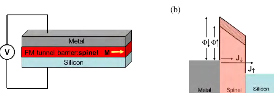
Although perovskite oxides received most of the attention, spinels are also of high interest for spintronics. Some of them, including CoFe2O4 and NiFe2O4, are ferromagnetic at room temperature with high magnetization, and contrary to most ferromagnetic materials they are electrically insulators. Thus they offer new opportunities for spintronics. In particular, they can be used as active tunnel barrier in spin filter devices, where the tunnel probability depends on the spin of the electrons, see a sketch in figure I.5.
Chapter I : General introduction
5
(a) (b)
Figure I.5: Sketch of a spin filter device, where CoFe2O4 is used as active tunnel barrier (a), and of the spin injection in silicon through the spinel barrier (b).
Pioneering work with NiFe2O4 as ferromagnetic barrier demonstrated a spin-filtering efficiency of 23% at low temperatures [LUD06], and more recently it has been reported room temperature spin filtering in magnetic tunnel junctions (MTJs) containing CoFe2O4 tunnel barriers with tunnel magnetoresistence (TMR) values of 18% and 3% at 2 and 290 K, respectively [RAM07]. The use of functional oxides as CFO in electronics critically depends on the epitaxial integration with silicon, which requires a buffer layer to avoid chemical interaction and allows lattice matching. The use of yttria-stabilized zirconia (YSZ) as buffer layer, which was early investigated [FOR90], allows for a direct crystallization after reduction of the native silica, and become the most common buffer used to integrate functional oxides on silicon. For example, ferroelectrics as Pb(Zr, Ti)O3[GUE01, DEK10], or Bi3.25La0.75Ti3O12
[LEE02], and Bi3.15Nd0.85Ti3O12 [ZHA10] as well as ferromagnetic La2/3Sr1/3MnO3 and related manganites [FON99, KIM03, TRA96, PER09] and spinel oxides [WAK02-04] can grow epitaxially on YSZ buffered Si(001). It can be noted that YSZ films are epitaxially grown by pulsed laser deposition (PLD) [AGU97, FOR90] and do not require removal of the native silicon oxide. Indeed, their crystalline quality is enhanced compared to YSZ deposited on bare silicon [COP00, KIG02-03, WAN00-01]. Other oxides as γ-Al2O3 and SrTiO3 that can be used as buffers are usually grown by molecular beam epitaxy (MBE) on a SiOx-free silicon surface [MER06, MI_08].
I.1.4 Objectives of the thesis
The thesis aims at integrating CFO with silicon using different buffer layers. The ultimate goal being the fabrication of ultrathin CFO/buffer structures that could permit the fabrication of a spin filter device for spin injection in silicon.
The selection of the buffer layer is critical, since it has to allow the growth of high quality epitaxial layers of CFO and display high stability with silicon under the conditions used to deposit CFO. In a parallel study we have used SrTiO3, Sc2O3 and Y2O3 buffer layers fabricated by molecular beam epitaxy (MBE) by collaborators, as well as pulsed laser deposition (PLD)-grown ultrathin YSZ layers, developed during this thesis.
I.2 CoFe
2O
4The spinel CoFe2O4 is an electrical insulator that shows ferromagnetic order at room temperature with high magnetocrystalline anisotropy. In addition, it is a low cost and highly stable material.
Chapter I : General introduction
6
The ideal spinel structure is sketched in figure I.6 (the unit cell is formed by 8 cubes as the one shown). Oxygen atoms form a fcc lattice, and cations occupy interstitial tetrahedral and octahedral sites.
Figure I.6: Schematic representation of the spinel crystal structure [RIG10].
In the unit cell there are 8 divalent cations and 16 trivalent cations. There are three different structures of spinels: “normal”, “inverse” and “mixed”, which are distinguished in function of the cations position distribution on tetrahedral (A) and octahedral (B) positions. In the normal spinel type, divalent cations only occupy A-sites, while the trivalent cations are only present in B-sites (e.g. MgAl2O4, CoCr2O4 and other chromites). In the inverse spinel structure, divalent cation occupies B-sites, and trivalent cations equally distributed over A- and B- sites (e.g. NiFe2O4 and Fe3O4). The mixed structure is a combination between the normal and the inverse structure (e.g. (Mn,Zn)Fe2O4).The respective general formula of these type of spinel are: 2
3 2 4 ) (M A N BO ,
4 3 2 3 ) (N A M N BO , and
4 3 2 2 3 2 1 ) (M N Mx N x BO A x x where 0<x<1.In their bulk form, most of spinel ferrites are electrical insulators, and thus ultrathin films of spinel ferrites could be ideally used as insulator layer for spin polarized tunnel transport. The spin filter efficiency of an ideal ferrite barrier depends on its thickness, and it is predicted that a barrier thickness of less than 2 nm is large enough to ensure a full polarization (negative) of the tunnelling current [MOO88-10].
CoFe2O4 has an inverse spinel structure, assimilated to a CFC structure with a Fd-3m symmetry group and a lattice parameter of 0.839 nm. The unit cell contains 32 oxygen atoms, 64 tetrahedral sites (A) and 32 octahedral (B) sites with respective occupation fractions of 1/8 and 1/2. The tetrahedral (A) sites are occupied exclusively by Fe3+ cations and octahedral (B) sites by both Fe3+ and Co2+. The A or B-site position of the cation defines the number of nearest neighbours, which is 4 in the A-site position and 6 in the case of B-site occupancy. The distance between cations varies from 0.297 nm for B-B neighbours, to 0.348 nm for A-B neighbours, and 0.365 nm for A-A neighbours (considering a 0.84 nm unit cell).
The atomic stacking sequence in the [001] direction are A-planes of Fe3+ alternated with B-planes of Fe3+ and Co2+, while in the [111] direction oxygen planes are intercalated with A and B planes (OBOABAOBO).
Chapter I : General introduction
7
Figure I.7: Sketch of the atomic stacking along [001] and [111] directions [GAT04].
CFO is an electrical insulator and ferromagnetic at room temperature with a Curie temperature of Tc= 793K [KIN00]. It has very high magnetocrystalline anisotropy and very high magnetostrictive coefficients (λ100= -590.10-6 and λ111=120.10-6) [BOZ55, STU69]. Magnetic properties can be modified by ion substitutions [BOZ55, TAC60] or epitaxial strain
[HU_00].
The resistivity ρ of a 100 nm CFO thin film at room temperature is 2.66 × 10⁴ Ω·cm [RAI11]. The insulating character for epitaxial thin films (t ≈15 nm) was demonstrated to be preserved, although with highly reduced resistivity values (around of 102 Ω·cm at room temperature and around 106 Ω·cm at 150 K) [RAM07-08]. Integrating ultrathin films of CFO on silicon, with the total thickness of the system a few nm, could allow a magnetic tunnelling barrier for spin polarized electron injection on silicon although the low resistivity at room temperature could be a serious limitation.
Considering the growth of CFO film, the surface energy is a main parameter. Surface energy values for CFO are not reported, but data of related spinels as Fe3O4 and NiFe2O4 [MIS77]
can be taken as a reference. The surface energy is highly anisotropic, with {111} planes having a surface energy factor lower than the {001} ones.
I.3 Oxides on silicon
Silicon has a cubic diamond structure, with lattice parameter a= 5.43088 Å. The atomic interspacing along the diagonal of a face,a/ 2= 3.84 Å, is close to perovskites lattice parameter (aSTO= 3.905 Å). It has a low thermal expansion coefficient of 2.3.10-6 K-1 generally smaller than complex oxides [FUK11]. The growth of oxide thin films on silicon has been extensively studied, mainly for the development of high-k materials, and many of them can be successfully integrated [KIN00, MI_08, REI10]. In contrast, most of complex functional oxides cannot be grown directly on silicon due to the structural mismatch and/or chemical interaction, and then the use of a buffer layer is required. It represents a difficulty, but even for applications ideally requiring direct complex oxide/Si interface, the use of ultrathin buffer can maybe permit epitaxy being compatible with the application.
The silicon wafers are covered by amorphous SiO2 which could hinder the epitaxial growth. The native amorphous silica can be removed by chemical etching (HF), thermal treatment in UHV, or if can be reduced by depositing atoms with strong affinity to oxygen. The growth of a crystalline oxide typically requires high temperature and presence of oxygen in the vacuum
Chapter I : General introduction
8
chamber. There is interaction between silicon, oxygen and the oxide cations, and thus different chemical reactions are possible. Thermodynamics, comparing the Gibbs energy in the reaction causing formation of the desired oxide with others reactions forming silicides or silicates, is to be considered to rationalize the growth. However kinetics and limitation in the amount of oxygen or cations can be highly relevant opening the possibility to develop growth strategies to avoid formation of energetically-favoured interfacial compounds.
Temperature and oxygen pressure are crucial parameters. As an example, the Motorola method, developed to grow epitaxially SrTiO3 by molecular beam epitaxy, includes several steps that are critical to obtain an atomically sharp interface. Indeed, SrTiO3 is thermodynamically unstable in contact with silicon at 1000K: 3Si + SrTiO3→SrSiO3 + TiSi2 (ΔG= - 19.133 kcal/mol) [HUB96], but extensive experimental studies have reveled that an intermediate epitaxial SrO monolayer permits epitaxial integration of SrTiO3with Si (SrTiO3/ SrO/ Si) [KEE98, Li_93, MOR91, YU_00].
The optimal method of preparation is different for other oxides and moreover can depend on the specific deposition technique used, but there are some common trends. In particular, the excess of oxygen may lead to interface oxidation creating SiOx or silicate phases by diffusion through the oxide layer, while an oxygen-deficient environment could lead to silicides and oxygen vacancies in the thin film. The sketch presented in figure I.8 shows possible binary oxide/silicon interfaces.
Figure I.8: Sketch representing the possible silicon interfaces with oxides: (a) atomically sharp, (b) silicon oxide, (c) silicate, (d) silicide, adapted from [STE04].
I.3.1 Metal oxide/Silicon interface: thermodynamics
Before the experimental demonstration of an atomically sharp interface between Si and SrTiO3 [KEE98], Schlom and co-workers [HUB96] analysed tabulated thermodynamic data (Gibbs energy changes) of possible reactions between Si, O, and different metals. They reported additional information in a latter paper [SCH02]. Most metal oxides are not thermodynamically stable in contact with silicon, giving a failed balance reaction of the type: Si + MOx → M + SiO2 (ΔG<0), unless a few on them including ZrO2. In some cases the lack of tabulated ΔG data did not permit a prediction.
Moreover in a M-Si-O system, further reactions are possible, in particular those causing silicide and/or silicate formation:
Si + MxOy → MxSi + SiO2 Si + MxOy → M + MxSiOy Si + MxOy → MxSiy + MxSiOy
Chapter I : General introduction
9
As mentioned above, the thermodynamic analysis indicates, as pointed out in the pioneering work of Hubbard and Schlom [HUB96], a driving force for reaction, but kinetic barriers can prevent it. The analysis only included volume free energies, neglecting interface energies and reaction involving gaseous species. A discussion on their role can be found in the reviews
[LOC06, STE04].
Functional oxide films, usually with complex stoichiometry, rarely will be stable with silicon. Also, lattice mismatch can be high causing high interface energy in case of sharp interface, which would add other driving force for decomposition or reaction. Thus, a buffer layer is generally required. Candidates are in principle all oxides that can be grown epitaxially on silicon. One of the most popular, used from the early 90’s, is yttria-stabilized zirconia (YSZ). Later, the research on high-k oxides demonstrated the epitaxial growth of other oxides, being SrTiO3 the best example. SrTiO3 is moreover, as single crystal, the most popular substrate to deposit functional perovskites. But the list of candidates is longer, including for example CeO2, ZrO2, HfO2, Y2O3, Al2O3, Gd2O3 [HUB96, LOC06, SCH02, STE04]. Within the candidates, the choice of the material to be used as buffer layer to deposit a specific functional oxide has to consider the crystal compatibility (structure and lattice mismatch), eventual chemical interaction, and thermal expansion mismatch. The buffer role is to act as a nonreactive diffusion barrier and a stable nucleation template for the epitaxial growth of the functional oxide. Thermal expansion mismatch arises because most of the oxides have much higher thermal expansion coefficients than silicon. It must be minimized to prevent cracking due to induced tensile stress upon cooling. On the other hand, for some applications the buffer layer must be stable not only at the temperature of its growth, but also at the temperatures used for the growth of additional layers. In many cases, functional oxides are deposited at temperatures higher than 800 ºC. This can result in formation of interfacial SiOx or silicate layers that probably will not impede epitaxial growth of the functional film. However, this can be a serious limitation if the application requires very close proximity between silicon and the functional layer.
III.3.2 Incompatibility of CoFe2O4 with silicon
In the case of the ternary oxide CoFe2O4, as for binary oxides, the analysis of thermodynamic stability is not so straightforward. It has to include the binary oxides that can be formed with the present metals, Co and Fe (CoFe2O4 is deposited from vapor phase, and thus atomic Fe and Co arrive to the Si surface).
Considering Fe, there are three binary oxides that are solid at 1000K: FeO, Fe3O4 and Fe2O3
[SCH02]. Possible reactions between these oxides and Si are:
2
1
Si + FeO → Fe +2
1
SiO2 (ΔG1000 K= -158.138 kJ/mol) 2Si + Fe3O4 → 3Fe + 2SiO2(ΔG1000 K= -668.326 kJ/mol)2
1
Si + Fe2O3 → 2Fe +2
3
SiO2 (ΔG1000 K= -534.693 kJ/mol)The high value and ΔG<0 indicates that all these binary oxides are highly unstable with silicon. Cobalt oxides are also highly unstable. For example, cobalt silicide formation can occur by Co + 2Si → CoSi2 at 500°C. These data are in agreement with the low structural quality reported for CFO films directly grown on silicon [ZHO07]. The need to use of a buffer layer to integrate CFO on silicon is then clear.
Chapter I : General introduction
10
I.4 Outline of the thesis
First of all, the principal experimental techniques used in this work are presented in chapter II. Physical thin film deposition methods are introduced, with a special attention to pulsed laser deposition, the technique used to integrate CFO on silicon with different buffers layers: STO, YSZ, Sc2O3 and Y2O3.The in-situ RHEED monitoring is introduced, and a quick review of the ex-situ characterization techniques is presented (XRD and Φ-scan) with a brief comparison of X-rays and electron diffraction.
The description of transmission electron microscope is presented in annex A with its different modes and techniques. The image mode is detailed for low and high resolution, and EELS and EDXS spectroscopies are described and compared in annex B. The TEM experimental part aims to understand the origin of image contrasts and artefacts leading to a coherent interpretation. A detailed part is dedicated to the TEM sample preparation, with its challenges and alternative variations to overcome the sample degradation.
Chapter III presents the study of the STO buffer use to integrate CFO with Si(001). The STO film grown by MBE at INL-Lyon was structurally characterized at ICMAB, previously to the CFO integration. Both films grown in a two-step elaboration process are epitaxial. Detailed HRTEM analysis is presented as well as a chemical analysis by EELS, which shows Ti diffusion into the CFO layer.
Yttria-stabilized-zirconia (YSZ) as alternative buffer for the integration of CFO with Si(001) is studied in chapter IV. The mechanisms of epitaxy of YSZ were investigated and ultrathin films (~2 nm) were fabricated with very small amount of SiOx (<1 nm) at the interface. CFO grows epitaxially on YSZ, with (111) out-of-plane orientation. Extremely thin CFO/YSZ bilayers were fabricated, being the SiOx interfacial layer around 2 nm.
Sc2O3 and Y2O3 films deposited on Si(111) by MBE at IHP-Frankfurt, have been also used and are studied in chapter V. They present huge lattice mismatch with CFO, but domain matching epitaxy permits high structural quality of CFO. Highly relevant, the Y2O3/Si(111) interface is stable after CFO growth. We show that ultrathin (t < 2 nm) Y2O3 buffers permit epitaxy of CFO.
Other characterization techniques used in this work are presented (AFM, SQUID) in annex C, and growth generalities and concepts definition about interfaces and dislocations are detailed in annex D.
Chapter II: Experimental techniques
11
Chapter II
Experimental techniques
II.1 Elaboration techniques
Techniques of fabrication of thin films are usually categorized in two groups: CVD (Chemical Vapour Deposition) and PVD (Physical Vapour Deposition). The first one uses materials reacting in their vapour phase, and the second uses a physical process to extract atoms from a solid. The physical techniques used in this work are molecular beam epitaxy (MBE) for some buffers layers (SrTiO3, Sc2O3 and Y2O3 buffers), and pulsed laser deposition (PLD) to grow YSZ buffers layers and thin films of CoFe2O4.
In this chapter, the MBE technique is briefly introduced, and PLD is described in more details.
II.1.1 Molecular beam deposition (MBE)
MBE is an ultrahigh vacuum deposition technique consisting on molecular evaporation of the constituent elements from one or more effusion cells to a heated substrate. MBE growth is carried under conditions out of the thermodynamic equilibrium and is conditioned by the kinetics of the surface processes. The thin film crystallisation is low enough to allow surface migration of species. The growth rate is typically less than 1ML/s and the surface of the grown film can be very smooth. MBE is applicable to the epitaxial growth of a wide variety of materials and in this thesis we have used some MBE deposited oxides as buffers layers. In particular, collaborators at IHP (Frankfurt-Oder, Germany) have provided Sc2O3 and Y2O3 films, and collaborators at INL (Lyon, France) SrTiO3 films.
II.1.2 Pulsed Laser Deposition (PLD)
The technique of PLD is illustrated schematically in figure II.1.
Chapter II: Experimental techniques
12
It is based on the use of proper laser radiation directed through a window on a ceramic target placed in a vacuum chamber, to create a plasma that will be deposited on a substrate. A main characteristic of the technique is that the stoichiometry of the target, excluding highly volatile species, will be transferred to the substrate. This requires however some characteristics of the radiation arriving to the target: wavelength in the ultraviolet, pulsed (tens of ns or shorter), and high energy density. In general excimer lasers are used, the most common ones being those using KrF. The wavelength is 248 nm (photon energy around 5 eV), and the repetition rate and pulse length are typically 1-10 Hz and 10-40 ns, respectively. Other excimer lasers, as the ArF (λ = 193 nm), Nd:YAG lasers, or ultra-fast lasers are much unusual. Ultraviolet radiation is necessary because optical absorption length (typically below 1 micron) is very short for most of materials, and then the radiation will be absorbed in the volume closest to the target surface. It is also necessary that the heat caused by the absorption stays confined very close to the irradiated area and very close to the surface. It implies that the thermal diffusion length has to be very short, and then the laser pulse has to be very short (tens of nanoseconds). The third requirement is that the energy exceeds a threshold that will cause that the atoms will be in a state totally out of the equilibrium, forming a plasma quickly
[WIL00]. Typical energy density (usually known as laser fluence) is 1-3 J/cm2, which is achieved by focusing the beam with a lens placed out of the deposition chamber. In addition the target needs to be moved during the process to reduce its erosion, otherwise its morphology will be finally non-uniform, with typical formation of cone-like structures that would result in non-stoichiometric evaporation [EAS07]. The process of irradiation under these conditions is usually known as ablation, and causes congruent etching of the atoms in the target. It is important to mention that the technique is not efficient for all classes of materials. For example, when metals or semiconductors are irradiated under the mentioned conditions they tend to eject liquid droplets. Detailed information on the mechanisms of laser-matter interaction for different classes of materials can be found at reference [CHR94]. PLD is particularly efficient to deposit oxides, and because ablation is congruent results particularly convenient to grow oxide films having more than one cation.
As mentioned, the target is inside a high or ultra-high vacuum chamber, and thus the plasma will expand quickly towards the substrate that usually is at a distance of 4-7 cm from to the target. The substrate holder permits heating it and it is usual to introduce oxygen in the vacuum chamber (typically from 10-4 to 0.5 mbar). It is necessary because although oxygen is present in the target (as example, stoichiometric ceramic targets of CoFe2O4 are used to deposit CoFe2O4 films), its high vapour pressure would cause loss in both target and substrate/film surface. On the other hand, the oxygen pressure permits to reduce the huge energy (up to hundreds of eV) that atoms and ions have when are ablated. Under vacuum the plasma would expand very quickly along the direction normal to the target (due to characteristic shape revealed by the emitted photons the plasma is known as “plume”). Increasing the pressure, the front of the plasma is decelerated (see in figure II.2 the effect of the pressure on CeO2 plumes).
Chapter II: Experimental techniques
13
Figure II.2: (a) Pictures of a PLD plume taken 4.5 μs after ablation of CeO2 for different oxygen pressures [TRT99].
The kinetic energy of the particles that arrive on the substrate will depend on the specific deposition condition, particularly the pressure, target-substrate distance, and laser fluence, but usually will be above the eV. This high energy is believed to enhance crystal growth compared to low-energy techniques [CHR08]. A distinctive characteristic of PLD is the pulsed deposition: after each laser pulse, atoms arrive on the substrate during few microseconds, with no additional arrival for a time of 1/f (f the laser frequency). This results in two different parameters, instantaneous and average growth rate, that can have different influence on the growth. A further advantage of PLD is that different deposition parameters (as oxygen pressure, temperature, and both instantaneous and average deposition rate) can be modified independently. Finally, PLD is compatible with the use of reflection high-energy electron diffraction (RHEED), thus permitting deposition with real time control. Indeed, sometimes PLD done with RHEED control is called as “laser molecular beam epitaxy”.
Figure II.3: (a) Schematic illustration of a PLD system with RHEED [RIJ07-1], and (b) picture of the used experimental set up at ICMAB.
Experiments were carried out in the thin film laboratory of the ICMAB laboratory (figure II.3). The laboratory owns two PLD deposition systems and the beam of an KrF excimer laser (wavelength of 248 nm, pulse duration around 30 ns, repetition rate up to 10 Hz, maximum energy per pulse 700 mJ) can be directed to each of them. They were fabricated by Twente Solid State Technology. The two systems dispose of load lock chamber and a multiple target holder to allow fabrication of multilayers in a single process. Both substrates and targets can be loaded via the load lock. The base pressure in both PLD systems is below 10-8 mbar, and the substrate heaters permit high deposition temperature (above 850 ºC) under oxygen and/or argon pressures.
Chapter II: Experimental techniques
14
One of the chambers integrates a RHEED system for growth dynamic studies and real-time control of the deposition. It uses an electron gun operated at 30 kV (in the experiments here reported) and two-differential vacuum stages that allow monitoring the growth under high-pressure oxygen up to 0.5 mbar.
II.2 Diffraction techniques
Diffraction by crystalline materials corresponds to the coherent scattering of radiation by a periodic structure of atoms. It only occurs if the wavelength has the same order of magnitude than the periodicity of the structure probed. The radiations used here are X-rays and electrons. After a description of the reciprocal space, we summarize the basics of diffraction and describe the particularities of diffraction by X-rays and electrons, in the latter for both reflection and transmission cases.
II.2.1 Theory of diffraction
A crystal is defined by its long order periodicity, with a repetition of its unit cell. This elementary volume “v” is defined in the real space by the base of vectors ⃗⃗⃗⃗ ⃗⃗⃗⃗ ⃗⃗⃗⃗⃗ , as ⃗⃗⃗⃗ ⃗⃗⃗⃗ ⃗⃗⃗⃗ . And atom positions can be described by ⃗ ⃗⃗⃗⃗ ⃗⃗⃗⃗ ⃗⃗⃗⃗ .
The reciprocal lattice is described with another vector base ⃗⃗⃗ ⃗⃗⃗⃗ ⃗⃗⃗⃗ . Where each vector is defined by par ⃗ ⃗⃗⃗⃗ ⃗⃗⃗⃗ ⃗⃗⃗⃗ ⃗⃗⃗⃗⃗ ⃗⃗⃗⃗⃗ , with i, j and k= 1, 2 or 3, and is orthogonal to two vectors of the direct base ⃗⃗⃗ ⃗⃗⃗ . ⃗⃗ is then defined by ⃗⃗ ⃗⃗⃗ ⃗⃗⃗⃗ ⃗⃗⃗⃗ , and more generally in the reciprocal lattice ⃗⃗⃗ ⃗⃗⃗ ⃗⃗⃗⃗ ⃗⃗⃗⃗ .
A family of lattice planes are determined by the integers (hkl) called Miller indexes. Equivalently, (hkl) denotes a plane that intercepts the three points a1/h,a2/k et a3/l in the direct lattice. The vector K is orthogonal to the hkl plans, and its length is the inverse of the interplanar distance.
The radiation interaction with atomic planes of a crystal is shown in figure II.4, where the incident rays are diffracted with an angle of θ. In the real lattice, the condition of constructive interference is given by the Bragg law: 2dsin n.
Chapter II: Experimental techniques
15
II.2.2 X-Ray diffraction
X-rays are electromagnetic waves interacting weakly with matter (at the considered energies).
Their wavelength has the same order of magnitude that the interatomic plane distances. Then, interplanar distances can be detected from the theta angle (Bragg law), at which there is diffraction, and this permits to identify crystalline phases, orientation, and lattice strain in the analysed materials. Most of the X-ray diffraction (XRD) analyses presented here have been performed at ICMAB using a 3-circles diffractometers Siemens D500, Rigaku Rotaflex RU-200B, and a 4-circle Bruker D8 equipped with a 2D detector. These diffractometers use Cu X-ray sources, which emission presents two lines called Kα1 (λ = 1.540562 Å) and Kα2 (λ= 1.544390 Å). Their relative intensity is 2/1, and because they are very close in wavelength is usual that their contribution to diffraction peaks from films is not resolved, and then an effective wavelength λ* = 1.541838 Å can be used for the analysis.
For an X-ray beam irradiating a set of crystallographic planes (hkl) the maximum intensity of the scattered beam occurs at an incidence angle according the Bragg law:
sin 2d(hkl)
Where dhkl is the interplanar spacing, and λ is the wavelength of the used source of X-rays. Two measurements geometries are presented in figure II.5: symmetric and asymmetric. In the symmetric configuration the diffraction planes are parallel to the sample surface, and in the asymmetric configuration the sample is oriented in order to obtain diffraction conditions for different planes non parallel to the sample surface.
Figure II.5: Sketches of the diffractometer used on symmetric (a), and asymmetric (b) configurations. The symmetric configuration θ-2θ adjustment is done with respect to the substrate. Χ and ω are adjusted to obtain a substrate symmetrical reflection. The experimental substrate and film spectra in the symmetric configuration present different peaks corresponding to atomic planes parallel to the surface. The substrate, being typically perfectly crystalline and thick, shows high intensity and narrow peaks, while the width of the film peaks is inversely proportional to the number of diffracting plans in the thin film. The angular location of the peaks in the spectra allows measuring the distance of the atomic planes in the direction perpendicular to the sample surface. In the case of textured films, a single family of planes is oriented perpendicular to the sample surface. In polycrystalline samples, different orientations can be observed in the spectra.
Other family planes tilted with respect to the sample surface can be measured with an asymmetric configuration of the system: (
2
2
, or tilting χ ) and orienting properly the sample along the in-plane direction.
Chapter II: Experimental techniques
16
The Φ-scans allow exploring the in-plane texture of the film by a sample rotation around the azimuthal angle Φ. In order to satisfy the Bragg condition for a certain asymmetrical reflection, the sample is tilted in the χ angle while keeping the ω= θ condition. This procedure allows determining the relative in-plane orientation between the film and the substrate and their epitaxial relationship. The combination of different Φ-scans taken with different values of ω leads to a pole figure which is a 2-dimensional Φ-ω map.
II.2.3 Electron diffraction
Both elastic and inelastic scattering are involved in electron diffraction techniques. Two theories, the kinematic one and the dynamical one, describe these processes. The kinematic theory considers that the incident beam is not attenuated after the diffraction phenomenon, and that its intensity is largely higher than the diffracted beams. Furthermore, the diffracted beams do not diffract themselves again, and their interaction with the incident beam is neglected. This theory is applied in most of the analysis of crystals such X-ray or neutron diffraction.
In the case of electron diffraction, the huge interaction with matter does not respect the kinematic approximation. Indeed, the incident beam can be attenuated by diffraction due to a higher thickness of the sample probed, presence of defects, etc, and multiple diffraction and interferences with other beams cannot be neglected. The diffracted beam can then have a higher intensity than the incident one, as in Bragg condition. A dynamic theory, taken into account these effects, is then described [COW81, REI84].
The kinetic approximation can be used to describe Bragg spots in electron diffraction patterns, but other features as Kikuchi lines require the dynamical theory.
II.2.3.1 Reflection High-Energy Electron Diffraction (RHEED)
Reflection High-Energy Electron Diffraction (RHEED) consists in sending an accelerated electron beam (10-100kV) in grazing incidence in the probed surface (up to 2°), and detecting the diffracted beams. This characterization technique allows checking the crystallinity and roughness of the surface. In-situ RHEED can be combined with a deposition technique, controlling the evolution of the thin film growth, from the first steps of the process. This is critical information to understand the growth mechanisms.
One of the chambers of the PLD systems at ICMAB integrates a RHEED system with two-differential vacuum stages that allow monitoring the growth under high-pressure up to 0.5 mbar. It used a 30 kV electron gun, and the substrate is up-side down, but the geometry is equivalent as the sketched below (figure II.6). The electron wavelength λ (Å) can be estimated by √ , with E in eV. The distance sample-phosphor screen is usually less than 30 cm, the incident angle ~ 0.5º <i< 3º, and the azimuth (in-plane) angle is adjusted to the desired axis zone.
Chapter II: Experimental techniques
17
Figure II.6: Schematic illustration of RHEED geometry. ΘI (ΘF) and ϕI (ϕF) are the incident and azimuthal angles of the incident (diffracted) beam. RS is the distance between substrate and phosphor screen and S the distance between the diffraction spots or streaks [RIJ07-2].
RHEED provides information about the periodic arrangement of the surface atoms, resulting in different types of patterns (figure II.7) depending on the crystallinity and the surface morphology.
Figure II.7: RHEED schematic patterns of different crystalline states of the surface [HYD06]. A diffuse halo is observed for amorphous surfaces, concentric rings for a polycrystalline state. For a single crystalline surface there is a pattern of Bragg spots along Laue circles. With moderate surface roughness they transform to vertical streaks, but with high roughness arrays of spots characteristics of 3D diffractions appear.
II.2.3.2 Transmission electron diffraction by TEM
The electron-matter interaction is very strong, as the electron beam interacts with the electrostatic potential of matter probed. Then, even using accelerated electron beams, the sample needs to be thinned down to several hundreds of nanometres for a transmission study. Considering an electron beam of 300 kV, the wavelength is 0.002 nm and the Ewald sphere diameter is 1000 nm-1 that can be considerated as a plane. In the particular case of transmission electron microscopy, the samples are so thin that the diffraction condition relaxes along the normal of the surface foil. This relaxation of the diffraction condition transforms the diffraction spots in relrods.
Chapter II: Experimental techniques
18
Figure II.8: Sketch of the intersection of the Ewald sphere with the reciprocal lattice showing the relaxation of the diffraction spots for thin samples.
The diffraction domains are reduced to fine sticks of 2/t length, where “t” is the sample thickness. Then, an excitation of a selective reflection hkl of non null intensity can occur when the Ewald sphere intersects with the correspondent diffraction domain, without necessarily passing by a node. K kk0 r*s, where s is the deviation of the Bragg position.
Ewald sphere intersect simultaneously several reciprocal planes, leading to circular and concentric Laue zones.
Figure II.9: Sketch of the Laue zones witch thickness depends on the relaxation conditions.
The most frequent diffraction mode used in TEM is the selected area of electron diffraction (SAED). A diaphragm inserted in the image plane of the objective lens is used to select a particular zone of the object in the image mode. Then, the diffraction diagram of this zone can be observed in diffraction mode. Electron diffraction phenomenon in TEM is really important to understand the high resolution contrast detailed in part III.2.2.
Radiation X-rays Electron beam
Technique XRD Φ-scan RHEED XS-TEM
Orientation (incident beam/sample) θ°/ atomic planes parallel to sample surface. Θ°/ atomic planes not parallel to sample surface. Grazing incidence (0-2°)/ surface Orthogonal to the thin film, the
substrate and their interface Sounded atomic
planes Out-of-plane
Non- parallel to
the interface Out-of-plane
In-plane & Out-of-plane λ (nm) 0.15406 (Cu) 0.0086 (20 kV) 0.00197 (300 kV) Resolution 0.01° 5% precision 0.1 nm Range 0-360° 10-100 kV 200-300 kV Quantitative
analysis 2dhklsinθ= λ a= λD/e
Direct measure (/ substrate) Table II.1: Characteristics of the different diffraction techniques.
![Figure II.3: (a) Schematic illustration of a PLD system with RHEED [RIJ07-1] , and (b) picture of the used experimental set up at ICMAB](https://thumb-eu.123doks.com/thumbv2/123doknet/2228743.15840/28.893.113.792.624.893/figure-schematic-illustration-pld-rheed-picture-experimental-icmab.webp)

![Figure III.8 presents RHEED patterns of the deposited CFO film, taken along [100] STO and [110]STO](https://thumb-eu.123doks.com/thumbv2/123doknet/2228743.15840/50.893.133.734.853.1044/figure-iii-presents-rheed-patterns-deposited-cfo-taken.webp)