Pépite | Fabrication et Caractérisation d’un transistor MOSFET III-V pour les applications de haute performance et de basse puissance
150
0
0
Texte intégral
(2) Thèse de Matej Pastorek, Lille 1, 2017. ii © 2017 Tous droits réservés.. lilliad.univ-lille.fr.
(3) Thèse de Matej Pastorek, Lille 1, 2017. Acknowledgements First and foremost, I would like to express a limitless gratitude to my thesis supervisors Sylvain Bollaert and Nicolas Wichmann for providing me a continuous support and encouragement throughout the course of my thesis research. Working with them was a great pleasure and I have truly enjoyed each discussion we had. In particular, I would like to thank Sylvain for having selected me as his Master student and then as his PhD student. Through countless project discussions, he created a supportive and constructive environment giving me chance to grow in my scientific skills and creativity. I will never forget the kindness and care for all his students. I owe special thanks to Nicolas who is one of the most experienced multi-facet scientist I have ever met. He has shared with us enormous skills and knowledge in fabrication, material science and electrical engineering. His unbelievable capacity to generate new ideas, anticipate problems and identify errors has enabled us to orient the project into the right direction. I would also take this opportunity to extend my thanks to Epiphy group that has provided us with high-quality epitaxies. In particular, I would like to express my gratitude to Ludovic Desplanque, Xavier Wallart and Maria Fahed for our exemplary collaboration on the development of MBE raised contact technology and FinFET InAs. Also, I cannot omit the contribution of Alain Bruno Fadjie for his oxygen plasma but also the help of Aurélien Olivier in finishing the fabrication process of the FinFET. Among the persons playing a crucial role in the device development should be also counted the IEMN engineering stuff of the fabrication and characterization facility. They provided us with an excellent service and support. Especially, I would like to put ahead an excellent characterization engineer Sylvie Lepilliet for having introduced me to the art of RF characterization. My special thanks are addressed also to my precious colleagues, namely to my “zen masters” Yoann Lechaux and Vinay Kumar for sharing their “shining frequencies” of stillness and joy. My thanks go also to Mohamed Ridaoui for his sense of humor, friendship, loyalty and for all the help. They are ones of the most exceptional human beings I have ever met.. iii © 2017 Tous droits réservés.. lilliad.univ-lille.fr.
(4) Thèse de Matej Pastorek, Lille 1, 2017. The final words are address to my precious friends: Gaston, Bertrand, Florian, Ange, Georgia, Clémentine and Eckhart for their love, care and kindness from the very beginning of this challenging journey. I can hardly imagine that without them I would have finished my thesis.. iv © 2017 Tous droits réservés.. lilliad.univ-lille.fr.
(5) Thèse de Matej Pastorek, Lille 1, 2017. v © 2017 Tous droits réservés.. lilliad.univ-lille.fr.
(6) Thèse de Matej Pastorek, Lille 1, 2017. Résumé La réduction de la taille des circuits CMOS vers des dimensions extrêmement petites est telle que son élément constitutif, le MOSFET à base de Silicium, commence à souffrir d’une faible efficacité de puissance. L’une des alternatives qui ne peut être écartée est le concept du transistor MOSFET à base de matériaux III-V. Ses propriétés de transport extraordinaires, apportées par les matériaux III-V, promettent de réduire la tension d’alimentation des circuits CMOS sans réduire leur performance. Cette transition technologique pourrait aboutir non seulement à des circuits CMOS plus petits, plus écologiques mais aussi à des circuits co-intégrés avec des technologies RF. C’est dans ce contexte que nous présentons, dans ce travail de thèse, la fabrication et la caractérisation des transistors MOSFET Ultra-Thin Body (UTB) à base d’InAs et du transistor FinFET à base d’InAs. La combinaison d’une longueur de grille extrêmement réduite, d’une faible résistance d’accès et d’une mobilité impressionnante dans le canal d’InAs a permis d’obtenir des courants importants (IMAX=2000mA/mm pour LG=25nm). Egalement, l‘utilisation des architectures du canal de type ultra mince et FinFET permet d’obtenir un bon contrôle électrostatique. De plus, une spécificité du procédé technologique présentée dans ce travail est les réalisations des contacts et du canal par une épitaxie par jets moléculaires (MBE) localisée. Mots-clés: Matériaux III-V, MOSFET, Ultra-Thin Body, Gate-All Around, FinFET, recroissance, MBE, ALD. Abstract Scaling the size of CMOS circuits to extremely small dimensions gets the semiconductor industry to a point where its cornerstone, Silicon-based MOSFET starts to suffer a poor power efficiency. In the quest for alternative solutions cannot be omitted a concept of III-V MOSFET. Its outstanding transport properties hold a promise of reduced CMOS supply voltage without compromising the performance. This can path a way not only to the smaller, greener electronics but also to more co-integrated RF and CMOS electronics. In this context, we present fabrication and characterization of Ultra-Thin body InAs MOSFETs and InAs FinFET. Synergy of a deeply scaled gate length, low access resistance and a high mobility of InAs channel enabled to obtain impressively high drain currents (IMAX=2000mA/mm for LG=25nm). Equally, the introduction of Ultra-Thin body and FinFET channel design provides an improved electrostatic control. A specific feature of the process presented in this work is a fabrication of contacts and channel by localized molecular beam epitaxy MBE epitaxy.. Keywords: III-V Material, MOSFET, Ultra-Thin Body, Gate-All Around, FinFET, regrowth, MBE, ALD. vi © 2017 Tous droits réservés.. lilliad.univ-lille.fr.
(7) Thèse de Matej Pastorek, Lille 1, 2017. Table of contents Acknowledgements .................................................................................................................................iii Résumé .................................................................................................................................................... vi Abstract ................................................................................................................................................... vi List of figures ............................................................................................................................................x List of abbreviations ............................................................................................................................... xv General Introduction ............................................................................................................................... 1 1. Power constrained scaling............................................................................................................... 1 Moore’s law ............................................................................................................................. 1 End of Moore’s law.................................................................................................................. 1 Beyond Silicon MOSFET ........................................................................................................... 3. 2. Thesis organization .......................................................................................................................... 3. Chapter 1 ................................................................................................................................................. 6 1. Introduction ..................................................................................................................................... 6. 2. Channel material for high-performance MOSFET ........................................................................... 6. 3. Theory of deeply scaled MOSFET .................................................................................................... 9 Gate command ...................................................................................................................... 10 3.1.1. Oxide Capacitance 𝑪𝒐𝒙 ................................................................................................. 11. 3.1.2. Inversion Capacitance (𝑪𝒊𝒏𝒗) ...................................................................................... 11. Transport theory ................................................................................................................... 14. 4. 3.2.1. Long channel Theory: pinch-off saturation ................................................................... 15. 3.2.2. Intermediately long channel theory: drift velocity saturation ...................................... 15. 3.2.3. Deeply scaled MOSFET: ballistic and semi-ballistic transport ....................................... 16. MOSFET off-state performance..................................................................................................... 18 Idealistic model ..................................................................................................................... 19 Non-idealistic model.............................................................................................................. 20. 5. 4.2.1. Interface traps ............................................................................................................... 20. 4.2.2. Tunneling leakages ........................................................................................................ 21. 4.2.3. Short channel electrostatic leakages............................................................................. 23. Architecture consideration............................................................................................................ 23 Bulk MOSFET ......................................................................................................................... 24 Two dimensional MOSFET ..................................................................................................... 25 Three dimensional MOSFET .................................................................................................. 26. 6. Overview of state of art MOSFETs................................................................................................. 27 Planar UTB (2D) III-V MOSFET ............................................................................................... 27 6.1.1. UTB III-V MOSFETs with alloyed S/D contacts ............................................................... 27 vii. © 2017 Tous droits réservés.. lilliad.univ-lille.fr.
(8) Thèse de Matej Pastorek, Lille 1, 2017. 6.1.2. UTB III-V recessed gate MOSFET ................................................................................... 28. 6.1.3. UTB III-V MOSFETs with selectively raised S/D ............................................................. 29. State of art III-V FinFET and GAA devices .............................................................................. 30. 7. 6.2.1. FinFET and GAA with top-down process ....................................................................... 31. 6.2.2. Fin FET and GAA with bottom-up process..................................................................... 32. 6.2.3. State of art Si MOSFET ................................................................................................... 33. Conclusion ..................................................................................................................................... 34. Chapter 2 ............................................................................................................................................... 36 1. Introduction ................................................................................................................................... 36. 2. Channel-substrate module ............................................................................................................ 36 Ultra Thin Body (UTB) 2D III-V channel ................................................................................. 38 Gate All Around (GAA) or FinFET 3D III-V channel ................................................................ 39. 3. Gate stack module ......................................................................................................................... 40 ALD deposition ...................................................................................................................... 40 Oxide defects ......................................................................................................................... 41 Passivation technique............................................................................................................ 42 Extraction of Dit ..................................................................................................................... 43 3.4.1. HF-LF method ................................................................................................................ 43. 3.4.2. Conductance method .................................................................................................... 44. Effect of MOSFET process related contamination ................................................................ 45 3.5.1 4. MOSCAP fabrication process ......................................................................................... 46. Source and drain contact module ................................................................................................. 50 Selectively raised source and drain ....................................................................................... 51. 5. 4.1.1. Contact uniformity ........................................................................................................ 52. 4.1.2. Selectivity ...................................................................................................................... 54. 4.1.3. Extraction of the contact resistance.............................................................................. 55. UTB InAs MOSFET fabrication module .......................................................................................... 58 Presentation of UTB InAs MOSFET mask ............................................................................... 58 UTB InAs MOSFET process flow............................................................................................. 60 Hard mask patterning ............................................................................................................ 64 5.3.1. EBL dose determination ................................................................................................ 64. 5.3.2. HSQ adhesion ................................................................................................................ 65. Impact of selected wet chemical treatments on MOSFET UTB epi layer .............................. 66 5.4.1. NH4OH treatment .......................................................................................................... 66. 5.4.2. TMAH treatment ........................................................................................................... 67. 5.4.3. HCl Treatment .............................................................................................................. 68. 5.4.4. HF Treatment................................................................................................................. 68 viii. © 2017 Tous droits réservés.. lilliad.univ-lille.fr.
(9) Thèse de Matej Pastorek, Lille 1, 2017. 6. GAA (FinFET) InAs fabrication module .......................................................................................... 69 Presentation of GAA (FinFET) InAs mask ............................................................................... 70 GAA (FinFET) InAs MOSFET process flow .............................................................................. 71 Impact of device orientation on channel and contact uniformity ........................................ 74 Chemical Analysis .................................................................................................................. 77. 7. Conclusion ..................................................................................................................................... 80. Chapter 3 ............................................................................................................................................... 81 1. Introduction ................................................................................................................................... 81. 2. First MOSFET generation ............................................................................................................... 81 Impact of selectively raised S/D InAs n+ design .................................................................... 82. 3. Second MOSFET generation .......................................................................................................... 90 Bilayer oxide Al2O3 + HfO2 ...................................................................................................... 92 Hybrid device orientation ...................................................................................................... 95 Impact of epi-layer quality .................................................................................................. 100 Decomposition of UTB InAs MOSFET source and drain InAs n+ access resistance ............. 105 Interface and Ballistic resistance ......................................................................................... 107. 4. Third MOSFET generation ........................................................................................................... 108 Decomposition of the access resistance of MOSFET with raised S/D InGaAs n+ ................ 109. 5. First FinFET generation ................................................................................................................ 114. 6. Conclusion ................................................................................................................................... 119. General Conclusion and Perspectives ................................................................................................. 120 Appendix.............................................................................................................................................. 124 1. Microwave characteristics........................................................................................................... 124 UTB InAs MOSFET ................................................................................................................ 125 FinFET InAs .......................................................................................................................... 126. References ........................................................................................................................................... 127 List of publications............................................................................................................................... 133. ix © 2017 Tous droits réservés.. lilliad.univ-lille.fr.
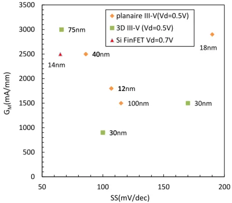
(10) Thèse de Matej Pastorek, Lille 1, 2017. List of figures Figure 1: Active power consumption and leakage (subthreshold) power density [4]. ........................... 2 Figure 2: Evolution of III-V MOSFET at Institute of Electronics Microelectronics and Nanotechnology (IEMN) with outlined topology of devices presented in this work. ........................................................ 5 Figure 3: Velocity characteristics of electrons and holes in electric field. The low field slope of carrier velocities in GaAs is lower than the slope in Si material [12]. ................................................................ 7 Figure 4: Experimental electron injection velocity extracted from III-V and Si FET devices. Reported mobility in strained Si is two times lower than in In(Ga)As based FETs [13]. ......................................... 8 Figure 5: Equivalent gate capacitance circuit diagram of confined InAs quantum well channel. Orange line corresponds to the charge concentration with a characteristic centroid form induced by the quantization effects............................................................................................................................... 10 Figure 6: Calculated 𝐶𝑖𝑛𝑣𝐷𝑂𝑆 as a function of sheet charge density for Si and InAs electron transversal effective masses. ................................................................................................................................... 13 Figure 7: Calculated electron injection velocity as a function of the sheet density for InAs and Si channel. ................................................................................................................................................. 17 Figure 8: MOSFET transfer (sub-threshold) characteristic with outlined MOSFET operation regions. 19 Figure 9: MOSFET capacitance model with outlined parasitic and ideal MOS capacitances............... 20 Figure 10: Illustrated leakage mechanism of MOSFET bipolar gain effect ........................................... 22 Figure 11: Transition from bulk to 2D and to 3D design. New designs converge towards a better electrostatic control of channel [36]. .................................................................................................... 25 Figure 12: Example of SS versus 𝛼 for different category of MOSFET designs [38] ........................ 26 Figure 13: Cross sectional TEM images extremely scaled 20 nm LG MOSFET with Ni alloyed S/D [42].28 Figure 14: Output characteristic of InAs-OI n-MOSFETs with LG of 20nm with Ni alloyed S/D [42]. ... 28 Figure 15: Cross-sectional TEM image of LG 30nm MOSFET fabricated by recessed gate process [50]. ............................................................................................................................................................... 29 Figure 16: Output characteristic of 20nm LG MOSFET fabricated by recessed gate process [49] .... 29 Figure 17: Cross-sectional TEM image of 12nm LG MOSFET with MOCVD raised S/D [63] .................. 30 Figure 18: Output characteristic of 12nm LG MOSFET with MOCVD raised S/D [63].......................... 30 Figure 19: SEM image of stand-alone InGaAs fin patterned by RIE etching [67]. ................................. 31 Figure 20: Output characteristic of 30nm LG nanowire MOSFET patterned by RIE etching. The Fin FET width is equal to 22nm [67]. ................................................................................................................. 31 Figure 21: Schematic illustration of vertical InAs Nanowire FET [71]. .................................................. 32 Figure 22: Output characteristics of vertical InAs nanowire with a diameter of 45nm and LG= 200nm [71]. ....................................................................................................................................................... 32 Figure 23: Top-down SEM (a) and cross section (b) illustration of InGaAs GAA MOSFET. Channel and S/D contacts are formed by MOCVD regrowth [76].............................................................................. 33 Figure 24: Output characteristics of MOSFET with LG=75nm and Wf= 90nm. Channel and S/D contacts are formed by MOCVD regrowth [76] ................................................................................................... 33 Figure 25: Cross-sectional image of Intel’s 14 nm gate length FinFET [8]. ........................................... 34 Figure 26: Intel’s 14nm I-V characteristics [8]....................................................................................... 34 Figure 27: Comparison of Ion versus IOFF for the state of art Si and III-V MOSFET with LG<12-100nm) reported in this work. ........................................................................................................................................... 35 Figure 28: Comparison of GM versus SS for LG<12-100nm) for state of art MOSFET reported in this work. 35 Figure 29: High mobility 2D InAs channel integrated on a lattice mismatched InP substrate.............. 38 Figure 30: High mobility InAs 3D nanowire integrated on a lattice mismatched InP substrate. .......... 38 Figure 31: Energy band gap diagram (a) traced across the gate stack and channel heterojunction of the UTB InAs MOSFET (b). ........................................................................................................................... 39 x © 2017 Tous droits réservés.. lilliad.univ-lille.fr.
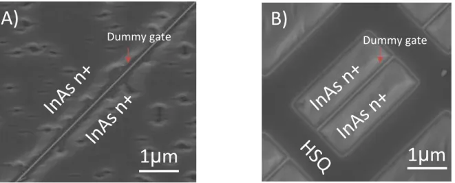
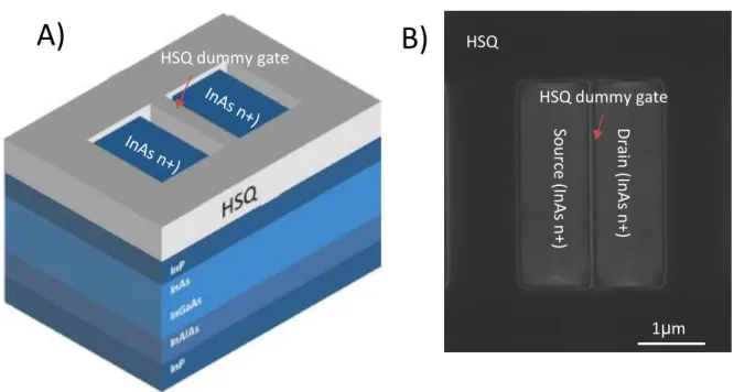
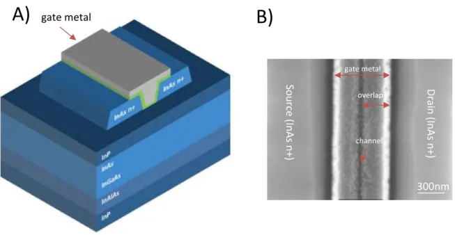
(11) Thèse de Matej Pastorek, Lille 1, 2017. Figure 32: Schematic illustration of the Atomic Layer Deposition (ALD) process................................. 41 Figure 33: Frequency dispersion of C-V curves measured in frequency range from 75Hz to 1MHz on Al2O3/InP MOSCAP without (a) and with (b) O2 plasma. Total Al2O3 thickness is 8nm (courtesy of Alain Bruno Fadjie) ......................................................................................................................................... 43 Figure 34: Equivalent circuits models for LF (a) and HF (b) signals. (HF-LF method)............................ 45 Figure 35: Equivalent circuit model for conductance method (a). Simplified circuit (b) of equivalent circuit (a) and measurement circuit (c). ................................................................................................ 45 Figure 36: Schematic illustration of the MOSCAP design. .................................................................... 46 Figure 37: (Sample A) C-V frequency dispersion curves. Measured frequency ranges between 100Hz and 1MHz (a) and Dit versus voltage extracted by conductance and HF-LF methods (b) ..................... 47 Figure 38: (Sample B) C-V frequency dispersion curves. Measured frequency ranges between 500Hz and 1MHz (a) and Dit versus voltage extracted by conductance and HF-LF methods (b). .................... 49 Figure 39: (Sample C) C-V frequency dispersion curves. Measured frequency ranges between 500Hz and 1MHz (a) and Dit versus voltage extracted by conductance and HF-LF methods........................... 49 Figure 40: Illustration of MOSFET with raised InAs n+ source and drain. Model of one side access resistance. ............................................................................................................................................. 52 Figure 41: Top-down SEM image of InAs n+ surface recorded after performing MBE growth (a) on a large surface through HSQ dummy gate. The InAs n+ surface is characterized by a low surface uniformity and by an absence of growth in the zone close to the dummy gate. (b) in HSQ 1x3μm apertures. The aperture is completely filled with a high-quality InAs n+. ............................................ 53 Figure 42: Top down SEM image recorded after InGaAs n+ growth with HSQ hard mask. HSQ surface is covered entirely by polycrystalline debris ............................................................................................ 54 Figure 43: Top down SEM image recorded after InGaAs n+ growth with an almost debris free HSQ surface ................................................................................................................................................... 55 Figure 44: Illustration of a typical TLM structure used in the dissertation for extraction of characteristic resistances of a raised source and drain contact module (a). Traced resistance of TLM structure with outlined elemental resistances. ............................................................................................................ 55 Figure 45: Lithography mask of UTB InAs MOSFET ............................................................................... 58 Figure 46: Design of two fingers (MOSFETs) measurement structure. ................................................. 59 Figure 47: Focus on MOSFET mask design. ........................................................................................... 59 Figure 48: Transmission line measurement structure .......................................................................... 59 Figure 49: Open and short circuit MOSFET structure utilized for RF de-embedding of parasitic elements. ............................................................................................................................................................... 59 Figure 50: Illustration (A) and top-down SEM image of localized selectively raised source and drain contact in HSQ pattern (B). ................................................................................................................... 61 Figure 51: Illustration (A) and top-down SEM image of the raised S/D and gate stack recorded (B) after the gate metal lift-off. ........................................................................................................................... 62 Figure 52: Illustration (A) and cross section STEM image (B) of the completed UTB InAs MOSFET with selectively raised InAs n+ S/D ................................................................................................................ 63 Figure 53: HSQ line exposed by a dose of 7000 μC/cm2. The mismatch between a designed and a real thickness is 50nm. ................................................................................................................................. 64 Figure 54: HSQ line exposed by a dose of 4800 μC/cm2. The mismatch between a designed and a real thickness is not detectable. ................................................................................................................... 64 Figure 55: Example of a collapsed HSQ structure after HF treatment and nitrogen drying ................. 65 Figure 56: Example of a free-standing HSQ structure after Ammonium hydroxide based solution and supercritical drying. ............................................................................................................................... 65 Figure 57: Scanned surface of the masked area (a) and the area exposed (b) to NH4OH solution. Measured step between (a) and (b) plane is around 0.5nm ................................................................. 67 Figure 58: AFM scanned surface exposed to NH4OH solution. The measured roughness RMS =0,42nm (RMS of virgin epi-layer is 0.48nm) ....................................................................................................... 67 Figure 59: Scanned surface of the masked area (a) and the area exposed to TMAH solution (b). ..... 67 xi © 2017 Tous droits réservés.. lilliad.univ-lille.fr.
(12) Thèse de Matej Pastorek, Lille 1, 2017. Figure 60: AFM scanned surface exposed to TMAH solution. The measured roughness RMS = 0,35nm (RMS of virgin epi-layer is 0.48nm) ....................................................................................................... 67 Figure 61: Scanned surface of the masked area (a) and the area exposed to HCl solution (b). Measured step between (a) and (b) plane. ............................................................................................................ 68 Figure 62: AFM scanned surface exposed to TMAH solution. The measured surface roughness RMS=0,41nm (RMS of virgin epi-layer is 0.48nm)................................................................................. 68 Figure 63: AFM Scanned surface of the masked area (a) and the area exposed to the HF solution (b). Measured step between (a) and (b) plane. ........................................................................................... 69 Figure 64: AFM scanned surface exposed to TMAH solution. The measured surface roughness RMS=0,42nm (RMS of virgin epi-layer is 0.48nm)................................................................................. 69 Figure 65: Lithography mask of GAA (FinFET) InAs ............................................................................... 70 Figure 66: Focus on GAA (FinFET) InAs mask design. ............................................................................ 70 Figure 67: Illustration (A) and top-down SEM image (B) recorded after the MBE of GaSb + InAs channel nanotemplates grown through SiO2 mask. ........................................................................................... 72 Figure 68: Illustration (A) and top-down SEM image (B) recorded after the second MBE InAs n+ regrowth on InAs channel. .................................................................................................................... 73 Figure 69: Illustration (A) and top-down SEM image (B) recorded after source, drain and gate metallization. ......................................................................................................................................... 74 Figure 70: Top down SEM images of InAs/GaSb channel nanotemplate grown in SiO2 apertures oriented along a) [110] b) [1-10] c) [100] direction. ............................................................................................ 76 Figure 71: Top-down SEM image recorded after HSQ development in TMAH that partially remove the underlying GaSb layer. Nanoribbons are oriented along a) [110] b) [1-10] c) [100] direction. ............ 76 Figure 72: Top down SEM image recorded after MBE selective regrowth of InAs n+ displayed in a) [110] b) [1-10] c) [100] direction. ................................................................................................................... 76 Figure 73: Top-down SEM image of [110] oriented InAs/GaSb nanostructures recorded after HSQ dummy gate removal. Dotted lines A and B depict InAs channel and InAs n+ contact profiles respectively. .......................................................................................................................................... 77 Figure 74: Cross-sectional image of InAs/GaSb channel nanotemplate oriented along [110] direction recorded by TEM (line A in Figure 73). (courtesy of Aurélien Olivier) ................................................ 78 Figure 75: EDX images of cross-sectional InAs/GaSb channel nanotemplate oriented along [110] direction. The color of As, In, Sb, P, Ga and O spectre is green, red, yellow, orange, purple and blue respectively. (courtesy of Aurélien Olivier) .......................................................................................... 78 Figure 76: Cross-section HAADF image of the second selective epitaxy of InAs n+ contact oriented along [110] direction. (courtesy of Aurélien Olivier) ...................................................................................... 79 Figure 77: Cross section EDX images of the second selective epitaxy of InAs n+ contact oriented along [110] direction. The color of Ga, Sb, In, As, P and O spectre is purple, yellow, red, green, orange and blue respectively. (courtesy of Aurélien Olivier) ................................................................................... 79 Figure 78: Key specifications of the 1st generation UTB MOSFET process ............................................ 82 Figure 79: Top-down SEM image of 3x3 μm2 HSQ apertures in which are selectively raised S/D InAs n+ contacts (a). Cross-sectional image of UTB InAs MOSFET realized with 3x3 μm2 InAs n+ contact module. The gate length exceeds HSQ dummy gate length designed to 50nm (b) ............................................ 83 Figure 80: Top-down SEM image of 1x3 μm2 HSQ apertures in which are selectively raised S/D InAs n+ contacts (a). Cross-sectional image of 50nm LG UTB InAs MOSFET realized with 1x3 μm2 InAs n+ contact module (b) ............................................................................................................................................. 84 Figure 81: Output characteristics (ID-VDS) of 50nm LG MOSFET with 3x3μm2 InAs n+ contact module. 84 Figure 82: Transfer characteristics (ID-VGS) of 50nm LG MOSFET with 3x3μm2 InAs n+ contact module. ............................................................................................................................................................... 84 Figure 83: Output characteristics (ID-VDS) of 50nm LG MOSFET with 1x3μm2 InAs n+ contact module. 85 Figure 84: Transfer characteristics (ID-VGS) of 50nm LG MOSFET with 1x3μm2 InAs n+ contact module. ............................................................................................................................................................... 85 xii © 2017 Tous droits réservés.. lilliad.univ-lille.fr.
(13) Thèse de Matej Pastorek, Lille 1, 2017. Figure 85: Subthreshold (log (ID)-VGS) and transconductance characteristics (GM-VGS) of 50nm (a) and 200nm (b) LG UTB InAs MOSFET with 1x3μm2 InAs n+ contact module. .............................................. 86 Figure 86: Plotted principal electrostatic parameters of 50, 100 and 200nm LG MOSFET as a function of LG. Threshold voltage (VDS = 0.7V) (a), Subthreshold swing (VDS = 0.7V) (b), Subthreshold swing (VDS = 50mV) (c), Drain induced barrier lowering (VDS = 50mV, 0.7V) (d). ....................................................... 89 Figure 87: Capacitance-voltage curves (f = 1MHz) of MOSCAPs containing 4nm Al2O3 and 2nm Al2O3 + 2nm HfO2 high-k oxides. ........................................................................................................................ 90 Figure 88: Key specifications of the 2nd generation UTB MOSFET process .......................................... 91 Figure 89: Subthreshold (log (ID)-VGS) and transconductance characteristics (GM-VGS) of 50nm (a) and 100nm (b) LG MOSFET. .......................................................................................................................... 92 Figure 90: Principal MOSFET electrostatic parameters. Threshold voltage (Vth) extracted at VDS=0.7V (a), Subthreshold swing (SS) extracted at VDS=0.7V (b), Subthreshold swing extracted at VDS=50mV (c), drain induced barrier lowering (DIBL) extracted at VDS=50mV and 0.7V (d). ....................................... 94 Figure 91: Output characteristics (ID-VDS) (a) and Subthreshold characteristics (log (ID)-VGS) (b) of 25nm LG MOSFET oriented along [1-10] direction. ......................................................................................... 96 Figure 92: Output characteristics (ID-VDS) (a) and Subthreshold characteristics (log (ID)-VGS) (b) of 25nm LG MOSFET oriented along [110] direction. ........................................................................................... 96 Figure 93: Output characteristics (ID-VDS) (a) and Subthreshold characteristics (log (ID)-VGS) (b) of 25nm LG MOSFET oriented along [100] direction. ........................................................................................... 97 Figure 94: Main MOSFET electrostatic parameters. Threshold voltage (Vth) extracted at VDS=0.7V (a), Subthreshold swing (SS) extracted at VDS=0.7V (b), Subthreshold swing extracted at VDS=50mV(c), Drain induced barrier lowering (DIBL) extracted at VDS=50mV and 0.7V (d). ................................................. 98 Figure 95: Cross-section STEM images of MOSFETs oriented along [110], |1-10] and [100] direction with depicted InAs n+ sidewall angles. ................................................................................................. 99 Figure 96: AFM surface scan on epitaxial layer InP/InAs/InGaAs/InAlAs/InP with RMS values 0.48nm (a) and 0.25nm (b). The scanned area is 0.5 x 0.5 µm². ...................................................................... 100 Figure 97: Cross-sectional high resolution TEM image of InP/InAs/ InGaAs/InAlAs/ epi-layers on InP substrate recorded after the device fabrication. ................................................................................ 101 Figure 98: Subthreshold (log (ID)-VGS) and transconductance characteristics (GM-VGS) of LG=100nm MOSFET grown on epi-layer of RMS roughness of 0.48nm (a) and 0.25nm (b)................................. 102 Figure 99: Principal MOSFET (RMS=0.48nm) electrostatic parameters. Threshold voltage (Vth) extracted at VDS=0.5V (a), Subthreshold swing (SS) extracted at VDS=0.5V (b), Subthreshold swing extracted at VDS=50mV (c), Drain induced barrier lowering (DIBL) extracted at VDS=50mV and 0.5V (d). ............................................................................................................................................................. 104 Figure 100: Illustrated model of one side access resistance (a) Plotted RON as a function of LG. (b) Plotted R obtained from the TLM structure (c) decomposed elements of the access resistance (d). ............ 106 Figure 101: Key specifications of the 3rd generation UTB MOSFET process flow ............................... 108 Figure 102: Output characteristics (ID-VDS) of 25nm LG UTB InAs MOSFET with InAs n+ (a) and InGaAs n+ (b) contact module. ........................................................................................................................ 109 Figure 103: Illustrated model of one side access resistance (a) Plotted RON as a function of LG. (b) Plotted R as a function of the separation gap L obtained from the TLM structure (c) decomposed elements of the access resistance (d). .................................................................................................................... 110 Figure 104: Subthreshold characteristic (ID-log(VGS)) of 25nm LG UTB InAs MOSFET with InAs n+ (a) and InGaAs n+ (b) contact module. ............................................................................................................ 111 Figure 105: Principal MOSFET electrostatic parameters. Threshold voltage (Vth) extracted at VDS=0.5V (a), Subthreshold swing (SS) extracted at VDS=0.5V (b), Subthreshold swing extracted at VDS=50mV(c), Drain induced barrier lowering (DIBL) extracted at VDS=50mV and 0.5V (d). ..................................... 113 Figure 106: Key specifications of the 1st FinFET generation process ................................................. 114 Figure 107: Cross-sectional STEM image of an array (a) and general view (b) of FinFET InAs channel with Ni/Au metal gate stack oriented along [110] direction............................................................... 115 Figure 108: Output characteristics (ID-VDS) of 200nm LG device. ......................................................... 116 xiii © 2017 Tous droits réservés.. lilliad.univ-lille.fr.
(14) Thèse de Matej Pastorek, Lille 1, 2017. Figure 109: Subthreshold characteristics (log(ID)-VGS ) of 200nm LG device ........................................ 116 Figure 110: Transfer characteristics (ID-VGS) of 200nm LG device. ....................................................... 116 Figure 111: Output characteristics (ID-VDS) of 1μm LG device. ............................................................. 118 Figure 112: Transfer characteristics (ID-VGS) of 1μm LG device. ........................................................... 118 Figure 113: Subthreshold characteristics (log(ID)-VGS ) of 1μm LG device ............................................ 118 Figure 114: Cross-section STEM image of UTB InAs MOSFET with raised InGaAs n+ contact module adapted for RF applications. Image is recorded before removal of sacrificial InP.............................. 123 Figure 115: De-embedded S parameters of 25nm LG MOSFET (a). Current ( 𝐻212) and Mason unilateral power gain (U) of 25nm LG MOSFET U plotted as function of frequency (b). (frequency range from 250MHz to 67GHz, VDS = 0.7V, VGS = max (H21)) .................................................................................. 125 Figure 116: Cut-off frequency ft displayed as a function of LG (a), maximum oscillation frequency fmax displayed as a function of LG (b). (frequency range from 250MHz to 67GHz, VDS = 0.7V, VGS = max (H21)) ............................................................................................................................................................. 125 Figure 117: De-embedded S parameters (a). Current ( 𝐻212) and Mason unilateral power gain (U) of 200nm LG FinFET (W=100nm) plotted as a function of frequency (b), (frequency range from 250MHz to 67GHz, VDS=1V, VGS=max (H21)) ............................................................................................................ 126 Figure 118: De-embedded S parameters (a). Current ( 𝐻212) and Mason’s unilateral power gain (U) of 1µm LG FinFET (W=200nm) plotted as a function of frequency (b), (frequency range from 250MHz to 67GHz, VDS=1V, VGS=max (H21)) ............................................................................................................ 126. xiv © 2017 Tous droits réservés.. lilliad.univ-lille.fr.
(15) Thèse de Matej Pastorek, Lille 1, 2017. List of abbreviations 2D 2DEG 3D AFM ALD BOE BTBT CBO CMOS CVD DC DIBL DOS EBL EDX EOT FinFET GAA GIDL. HBT HEMT HF-LF HMDS HP HRTEM. HSQ ICP-RIE IEMN IPA MBE MIBK MIT MOCVD MOS MOSFET MugFET NID PDA QW MOSFET RF RIE RMS RTA SBH. Two dimensional Two Dimensional Electron Gas Three dimensional Atomic Force Microscopy Atomic Layer Deposition Buffer Oxide Etch Band To Band Tunneling Conduction Band Gap Offset Complementary Metal Oxide Semiconductor Chemical Vapor Deposition Direct Current Drain Induced Barrier Lowering Density of States Electron Beam Lithography Electron Diffraction Spectroscopy Effective Oxide Thickness Fin shaped Field Effect Transistor Gate-All Around Gate Induced Drain Leakage Heterojunction Bipolar Transistor High Electron Mobility Transistor High Frequency Low Frequency Hexamethyldisiloxane High Performance High Resolution TEM Hydrogen silsesquioxane (resist) Inductively Coupled Plasma RIE Institute of Electronics Microelectronics and Nanotechnology Isopropanol Molecular Beam Epitaxy Methyl Isobutyl Ketone Massachussets Institute of Technology Metal Organic Chemical Vapor Deposition Metal Oxide Semiconducteur Metal Oxyde Semiconductor Field Effect Transistor Multiple Gate Field Effect Transistor Non Intentionally Doped Post Deposition Annealing Quantum Well Metal Oxyde Semiconductor Field Effect Transistor Radio Frequency Reactive Ion Etching Root Mean Square Roughness Rapid Thermal Annealing Schottky Barrier Height xv. © 2017 Tous droits réservés.. lilliad.univ-lille.fr.
(16) Thèse de Matej Pastorek, Lille 1, 2017. SCE SEM SOI SS TDMAH TEM TLM TMA TMAH ULP UTB VLS VLSI. Short Channel Effects Scanning Electron Microscopy Silicon On Insulator Subthreshold Swing Tetrakis-Dimethyl-Amido-Hafnium Transmission Electron Microscopy Transfer Length Measurement Trimethyl-Aluminium Tetramethylammonium hydroxide Ultra Low Power Ultra-Thin Body Vapor Liquid Solid Growth Very Large Scale Integration. xvi © 2017 Tous droits réservés.. lilliad.univ-lille.fr.
(17) Thèse de Matej Pastorek, Lille 1, 2017. General Introduction 1 Power constrained scaling Moore’s law During the last 50 years, we have been witnessing an incessant technological advance in microelectronics devices. Fifty years ago, a chip contained only dozens of gates whereas today the number has dramatically increased to several billions. This provided us with immense and complex circuits that are integrated into modern electronic devices. Such a huge progress was governed by Moore’s law formulated around 50 years ago. In the article “Cramming More Components onto Integrated Circuits” [1], Gordon Moore made a prediction that the number of transistor per chip would double every 24 months. Hereafter, the entire silicon industry has adopted his theory as a dogma that relentlessly dictates the trend of circuit miniaturization. The building block of today’s logical circuits is Complementary Metal Oxide Semiconductor (CMOS) technology consisting of p and n-type MOSFET transistor. Following Moore’s law and a CMOS scaling theory, its dimensions such as gate length, width and oxide thickness are reduced proportionally by a scaling factor (λ) equal to √2. Keeping a constant electric field in the channel implicates that a supply voltage (VDD) is reduced along with the MOSFET’s dimensions by a factor of λ. This is translated into an increased performance gain, proportional to λ, while the power density remains constant. End of Moore’s law However, scaling the CMOS technology below 90 nm gate length is characterized by a difficulty to reduce the device dimensions along with the supply voltage (V DD). Limiting factor starts to be a leakage power density [2][3] (Figure 1) that is related to the off-state current. Since the off-state current is exponentially dependent on the threshold voltage, the latter cannot be scaled proportionally with the supply voltage. On the contrary, decrease of the gate overdrive (VGS-VTH) would cause a degradation of the on-state current being related to the. © 2017 Tous droits réservés.. 1. lilliad.univ-lille.fr.
(18) Thèse de Matej Pastorek, Lille 1, 2017. General Introduction : Power constrained scaling. device switching speed. Nevertheless, constant channel voltage scaling affects the active power density that is proportional to VDD2. In this situation, the active power density increases as λ2 contrary to the unity in the constant electric field scaling. This would drastically increase the device consumption. Holding the clock frequency constant can only slow the increase of active power density by a factor of λ. In this situation continuing scaling inevitably leads to an increased chip power density. As a consequence, the chip temperature is raised what amplifies the off-state leakage currents. This vicious circle is referred as “Power constrained scaling” and makes the validity of Moore’s prediction questionable for next generations of CMOS devices.. Figure 1: Active power consumption and leakage (subthreshold) power density [4].. To overcome this limitation, novel technological solutions have been successfully introduced over the last decade. Stress engineering introduced for 90nm node allowed to enhance the channel carrier mobility [5]. Problematic oxide scaling was temporarily resolved with a high-k oxide applied in 45 nm node [6]. Also a successor of planar architecture, FinFET concept was introduced for 22nm node [7], followed by a second generation introduced for 14nm node [8].. © 2017 Tous droits réservés.. 2. lilliad.univ-lille.fr.
(19) Thèse de Matej Pastorek, Lille 1, 2017. General Introduction : Thesis organization. Beyond Silicon MOSFET Beyond the traditional Si MOSFET, multiple concepts of low power devices are available. Among them, we find tunnel FET [9], ferroelectric FET [10], mechanical switch [11]. A characteristic feature of this category of devices is an ability to obtain a smaller subthreshold swing than 60mV/dec reducing thus the off-state leakages. An alternative approach consists in replacing Si material by III-V high mobility materials. Here electrons can move from source to drain in much higher velocities than in Si MOSFET. Since the current is proportionally dependent on the carrier velocity, these materials have potential to deliver higher on-state current or in other words allow operation at a lower supply voltage. For decades, III-V technology has been successfully applied in High Electron Mobility Transistor (HEMT) and Heterojunction Bipolar Transistor (HBT) where they have shown an excellent dynamic performance and has become an inevitable part of RF applications. However, III-V MOSFET, has still not reached its predicted potential. High-quality III-V/ oxide interface, low access resistance but also an integration on Si substrate are the issues that have to be addressed before III-V materials could be implemented into CMOS circuits. In this context is presented the thesis that you are holding in your hands. It is organized as follows:. 2 Thesis organization The thesis will guide the reader through concept (Chapter 1), fabrication (Chapter 2) and finally through electrical characterizations (Chapter 3) of a deeply scaled Ultra-Thin body (UTB) III-V MOSFET and FinFET fabricated at Institute of Electronics Microelectronics and Nanotechnology in Lille. In Chapter 1, the theoretical concept of the deeply scaled MOSFET will be given. Specifically, in this chapter will be explained the notions such as mobility, injection velocity, MOSFET ballistic transport and why these are so important for a high-performance MOSFET operation regime. Furthermore, it will be discussed that a proper choice of architecture can diminish the leaky character of a deeply scaled MOSFET. Finally, it will be shown that despite. © 2017 Tous droits réservés.. 3. lilliad.univ-lille.fr.
(20) Thèse de Matej Pastorek, Lille 1, 2017. General Introduction : Thesis organization. an early stage of III-V MOSFET development, the concept features interesting on and off-state metrics. In the next step is presented the experimental part of the work: fabrication and characterization of Ultra-Thin body (UTB) InAs MOSFET and InAs FinFET (Figure 2). This work is a continuity of the first and second generation of III-V MOSFETs (Figure 2) previously fabricated at the Institute of Electronics Microelectronic and Nanotechnology in Lille (IEMN). Due to a high access resistance, these did not provide high on-state metrics and suffered from a bad scalability. In this situation, an update of architecture and fabrication process was vital to keep up with the technological advance of III-V MOSFET research groups. The most important change in fabrication represents the introduction of a localized Molecular Beam Epitaxy (MBE) realized in a close collaboration with our partner group Epiphy at IEMN. Regarding the architecture, Ultra-thin body (UTB) MOSFET and FinFET design were introduced. The practical part is presented in 2 chapters:. In chapter 2 are presented building blocks of the fabrication process. In the channelsubstrate section are presented epi-layers utilized for Ultra-Thin body (UTB) MOSFET and Gate-All-Around (FinFET) channel design. Description of the high-k oxide deposition is provided in the second section, the gate stack module. Formation of source and drain contacts based on a raised In(Ga)As n+ realized by localized MBE is discussed in the contact module. In the MOSFET and GAA (FinFET) fabrication modules, the reader can find a description of the devices fabrication schemes. In chapter 3 are discussed electrical characterizations of selected devices regrouped into 3 (sub)-generations of planar UTB InAs MOSFETs and 1 generation of InAs FinFET. The first (sub)-generation is characterized by the utilization of a single layer Al2O3 high-k oxide. A characteristic feature of the second (sub)-generation is the introduction of a bilayer high-k oxide Al2O3 + HfO2. Contrary to the previous (sub)-generations utilizing InAs +n S/D contact module, in the third (sub)-generation is used InGaAs n+ S/D contact module. Alternative channel architecture based on a suspended InAs channel was used in the last reported device referred as a first FinFET generation.. © 2017 Tous droits réservés.. 4. lilliad.univ-lille.fr.
(21) Thèse de Matej Pastorek, Lille 1, 2017. Figure 2: Evolution of III-V MOSFET at Institute of Electronics Microelectronics and Nanotechnology (IEMN) with outlined topology of devices presented in this work.. 5. lilliad.univ-lille.fr. © 2017 Tous droits réservés..
(22) Thèse de Matej Pastorek, Lille 1, 2017. Chapter 1 1 Introduction In this chapter, the reader can find the principal guidelines for designing a deeply scaled MOSFET. Firstly, we will explain basic notions such as mobility, carrier velocity and why these gauges are so important for high-performance MOSFETs. Furthermore, we will explain the underlying transport, command and leakage theory of a modern deeply scaled MOSFET that will be put into relation with the channel material and the channel architecture. Based on this, the reader should be capable to evaluate the advantages but also challenges of III-V MOSFET in comparison to a traditional Si MOSFET technology. Finally, the discussed theory is confronted with the current situation of III-V MOSFET. In the last section is presented a brief overview of the state of art experimental III-V MOSFETs and commercial Si MOSFETs.. 2 Channel material for high-performance MOSFET As outlined in the introduction, choice of channel material plays a crucial role in improving the n-MOSFET transport performance. Specifically, we have stated that III-V high mobility materials can deliver higher current for a given drain voltage than Silicon channel. This is enabled by a smaller electron effective mass that is inversely proportional to the carrier effective mobility. The former term reflects primarily existence of a periodical potential in a semiconductor crystal that is characterized by a specific energy dispersion diagram E(k). The role of the effective carrier mass is then to simplify the energy dispersion diagram by attributing to free carriers (electrons and holes) that occupy the conduction and valence band respectively a specific effective mass. This is quite a useful MOSFET gauge enabling to compare carrier velocities but also inversion capacitance with respect to a specific energetic level. When the semiconductor material is biased, free carriers get into motion acquiring a drift velocity that is inversely proportional to the carrier effective mass.. © 2017 Tous droits réservés.. 6. lilliad.univ-lille.fr.
(23) Thèse de Matej Pastorek, Lille 1, 2017. Chapter 1 : Channel material for high-performance MOSFET. Figure 3: Velocity characteristics of electrons and holes in electric field. The low field slope of carrier velocities in GaAs is lower than the slope in Si material [12].. In Figure 3 are illustrated GaAs and Si holes and electrons velocities dependency upon electric field. In a low field region (the region where the carrier velocity is linearly dependent upon electric field) GaAs shows a higher slope of v-E function than in Si what basically reflects a fact that light electrons can be accelerated to higher velocities compared to heavier electrons in Si material. Due to an increased carrier scattering with phonons, impurities, and crystal defects, the velocity in both materials is saturated and does not follow a linear dependency on the electric field. Here again, the GaAs attains higher values of maximum peak velocity at lower electric field than Si material. For the sake of clarity, we illustrate v-E function of merely GaAs but similar observation can be applied on the whole family of III-V materials that shows a superior electron drift and higher maximum peak velocities over Si. In this regard, we put ahead namely InAs that we choose as a channel material in this work. This exhibits an effective electron mobility of 40000 cm2(Vs)-1 what is almost 30 times higher than the effective electron mobility reported for Si channel (Table 1). Typically, light carrier, high carrier mobility and high maximum peak velocity are underlying preconditions to reach high on-state currents. Regarding the deeply scaled MOSFET, the device current is related to the injection velocity. Here also, a low effective electron mass is an underlying criterion to obtain a high injection velocity. More on this topic will be discussed in the section explaining the MOSFET transport theory.. © 2017 Tous droits réservés.. 7. lilliad.univ-lille.fr.
(24) Thèse de Matej Pastorek, Lille 1, 2017. Chapter 1 : Channel material for high-performance MOSFET. Figure 4: Experimental electron injection velocity extracted from III-V and Si FET devices. Reported mobility in strained Si is two times lower than in In(Ga)As based FETs [13].. In Figure 4 are illustrated typical injection velocities for III-V and Si FET devices. Transport properties of integrated III-V based FET are superior to MOSFET with strained silicon channel. In particular, injection velocities in InGaAs FET device are 2 times higher than velocities obtained in Si MOSFET. It is worth to note that this was obtained with 0.5V drain voltage compare to 1.3V obtained for Si MOSFET [13]. Regarding alternative material systems providing an outstanding carrier transport it is also worth to mention the graphene channel based FET (Table 1) that is explored namely in RF devices [14]. Despite its supreme transport properties, graphene misses a bandgap what induces a high off-state leakage current. Several solutions have been reported [15] trying to open the band gap but none of them has demonstrated a technological readiness. In this view, Graphene is very unlikely to become a material for CMOS logical switches. IV. Material parameter. III-V. 2D. Si. Ge. InAs. GaAs. In0,53Ga0,47As. Electron effective mass, me. 0,19. 0,08. 0,023. 0,063. 0,041. N/A. Hole effective mass mh. 0,49. 0,33. 0,41. 0,082. 0,45. N/A. Electron mobility (cm2 V-1s-1). 1400. 3900. 40000. 8500. 12000. 15000. 450. 1900. 500. 400. 300. 15000. Energy gap (eV). 1,12. 0,661. 0,354. 1,424. 0,74. Lattice constant (A). 5,431. 5,658. 6,06. 5,65. 5,8687. 2,45. 11,7. 16,2. 15,15. 12,9. 13,9. 16-3,3(HF). 1,3. 0,58. 0,27. 0,55. 0,05. 5. Hole mobility. (cm2. V-1s-1). Dielectric constant(εr) Thermal conductivity W. cm-1. °C-1. Graphene. N/A. Table 1: Parameters of Si and emerging material systems for FET devices [16][17].. © 2017 Tous droits réservés.. 8. lilliad.univ-lille.fr.
(25) Thèse de Matej Pastorek, Lille 1, 2017. Chapter 1 : Theory of deeply scaled MOSFET. The main advantage of III-V systems over alternative materials is its technological maturity [18]. Today, these are applied in the modern high-performance RF circuits as a part of HBT or HEMT devices. However, contrary to Si, materials such as InGaAs and InAs require integration on morphologically compatible substrates. Additionally, a narrow band gap InAs substrate would in MOSFET causes a high substrate leakage current. Also, it is not technologically feasible to grow a ternary compound substrate such as InGaAs. Therefore InAs and InGaAs are typically integrated on the conventional III-V substrates such as InP or GaAs [19]. Prior to the introduction of III-V materials in Very Large Scale Integrated Circuits (VLSI), several technological challenges have to be addressed. While the silicon as a channel material features inferior transport properties, it is still considered to be the best substrate material. Silicon has superior mechanical and thermal properties (Thermal conductivity of Si is 5 times higher than in InAs (Table 1) and most importantly, a lower price over III-V wafers. Hence, if III-V materials want to conquer VLSI market its ultimate co-integration on Si wafer is inevitable. Also, a major disadvantage of III-V lies in absence of a quality native oxide [20]. As a result, oxide gate stacks containing III-V semiconductor are prone to a high density of interface traps. Recently introduced Atomic Layer Deposition (ALD) technology enabled to deposit quality high-K dielectrics. Thanks to this technological breakthrough, III-V materials have gained the attention of engineering community as a feasible technology for future CMOS applications.. 3 Theory of deeply scaled MOSFET In this section is presented transport and command theory of a deeply scaled MOSFET. In a classical MOSFET, a gate stack capacitor is composed of metal, oxide and channel semiconductor. In principle, the structure modulates the carrier concentration in the channel. Accordingly, we can distinguish 3 operation regimes: inversion, accumulation and depletion. For n-type MOSFET a positive gate bias will repulse holes and attract negatively charged electrons in a thin layer referred as an inversion layer serving as a conducting path between the source and drain.. © 2017 Tous droits réservés.. 9. lilliad.univ-lille.fr.
(26) Thèse de Matej Pastorek, Lille 1, 2017. Chapter 1 : Theory of deeply scaled MOSFET. Gate command Gate stack ability to attract or repulse free carriers is characterized by a channel gate capacitance. For generations of MOSFETs with a thick oxide, the gate capacitance was equal to the insulator (oxide) capacitance. However, this does not hold for a deeply scaled oxide thickness requiring a more complex model accounting namely for the quantization effects. In Figure 5 is outlined an idealistic equivalent gate capacitance circuit diagram of a deeply scaled III-V Quantum Well (QW or UTB) MOSFET. This is composed of an oxide capacitance (𝐶𝑜𝑥 ), a 𝐷𝑂𝑆 𝑡ℎ𝑖𝑐𝑘𝑛𝑒𝑠𝑠 density of states capacitance 𝐶𝑖𝑛𝑣 and a centroid capacitance 𝐶𝑖𝑛𝑣 [21][22]. The model. does not account for process related parasitic terms such as an interface trap capacitance, oxide border trap capacitance, etc. that for a more realistic model of III-V channel MOSFET devices should not be disregarded. Considering the contribution of the abovementioned capacitances, we can write for the overall gate capacitance:. 1 𝐶𝐺. =. 1 𝐶𝑜𝑥. +. 1 𝐶𝑖𝑛𝑣. =. 1 𝐶𝑜𝑥. +. 1 𝐷𝑂𝑆 𝐶𝑖𝑛𝑣. +. 1 𝐶𝑡ℎ𝑖𝑐𝑘𝑛𝑒𝑠𝑠 𝑖𝑛𝑣. (1). Figure 5: Equivalent gate capacitance circuit diagram of confined InAs quantum well channel. Orange line corresponds to the charge concentration with a characteristic centroid form induced by the quantization effects.. © 2017 Tous droits réservés.. 10. lilliad.univ-lille.fr.
(27) Thèse de Matej Pastorek, Lille 1, 2017. Chapter 1 : Theory of deeply scaled MOSFET. 3.1.1 Oxide Capacitance (𝑪𝒐𝒙 ) The physical significance of the oxide capacitance is quite straightforward. It represents a capacitance of a standard dielectric layer that depends primarily on the oxide thickness and the oxide permittivity. Simply, thinner the oxide thickness, higher is the MOS capacitance and better is the channel electrostatic control. As a result, can be expected lower off-state current and higher on-state current. As a popular benchmark metrics is used Effective Oxide Thickness (EOT). This puts the dielectric constant and the oxide thickness in relation to SiO2 and is expressed as:. 𝐸𝑂𝑇. =. 𝜀𝑆𝑖𝑂2 𝜀ℎ𝑖𝑔ℎ 𝑘. 𝑡ℎ𝑖𝑔ℎ 𝑘. (2). 3.1.2 Inversion Capacitance (𝑪𝒊𝒏𝒗 ) For a deeply scaled oxide we observe a mismatch between the measured capacitance and the oxide capacitance. This is explained by an inversion capacitance (Cinv) that is wired in series with the oxide capacitance. As the oxide thickness becomes extremely thin, the weight of the inversion capacitance in the total channel gate capacitance grows while the weight of the oxide capacitance on the total capacitance is lowered. Consequently, when the oxide capacitance approaches the same order of magnitude as the inversion capacitance, the gain in electrostatic control driven by the oxide thinning is counterbalanced by a growing weight of the inversion capacitance. Accordingly, a larger value of Cinv is favorable for a more efficient gate command of an extremely scaled gate stack. Unlike the oxide capacitance, the physical significance of the inversion capacitance is not intuitive. It arises from an electron confinement in the inversion layer of Si MOSFETs [21] or in case of III-V MOSFET [22] from a thin quantum well confinement. In reality, the description of the effect is more complex as the quantification of states is manifested through two different effects. Each of them can be represented by a separate capacitance.. © 2017 Tous droits réservés.. 11. lilliad.univ-lille.fr.
(28) Thèse de Matej Pastorek, Lille 1, 2017. Chapter 1 : Theory of deeply scaled MOSFET. 3.1.2.1 Inversion Capacitance: Density of states capacitance (𝑪𝑫𝑶𝑺 𝒊𝒏𝒗 ) The carrier confinement in a Two-Dimensional Electron Gas (2DEG) system such as the inversion layer or a quantum well has one major bottleneck. This is a smaller density of states compared to 3D case. Filling the quantum well with carriers is accompanied by a raising Fermi level due to a finite Density of States (DOS) of each subband. Therefore, besides an energy required to create an electric field in the oxide, the creation of 2DEG will require an additional 𝐷𝑂𝑆 energy to raise the Fermi level. The relation between 𝐶𝑖𝑛𝑣 and 𝐸𝑓 − 𝐸1 is then formulated as. [22]:. 𝐷𝑂𝑆 𝐶𝑖𝑛𝑣 =. 𝐸𝑓 −𝐸1. Where. 𝑘𝑇. (. 𝑞2 𝑚 ∗ 𝜋ħ2. 𝐸𝑓 −𝐸1 𝑘𝑇. 1 + 𝑒−. (3). is referred as a Fermi reduced energy (𝜂) and can be obtained from 𝜂 =. 𝑁𝑆. ln (exp 𝑁2𝐷 − 1) and calculated with respect to the carrier concentration NS. Next, the expression. 𝑚∗ 𝜋 ħ2. stands for 2D DOS and is proportional to an electron effective mass. In the. 𝐷𝑂𝑆 following picture is plotted 𝐶𝑖𝑛𝑣 (Figure 6) as a function of carrier concentration for a low and. high electron effective mass (3).. © 2017 Tous droits réservés.. 12. lilliad.univ-lille.fr.
(29) Thèse de Matej Pastorek, Lille 1, 2017. Chapter 1 : Theory of deeply scaled MOSFET. 1. Capacitance(F/m). Density of states capacitance(CDOS) 0.1. InAs(m=0.026me) Si (m=0.98me). 0.01. 0.001. 0.0001 1E+10. 1E+11. 1E+12. 1E+13. 1E+14. NS (cm-2) 𝐷𝑂𝑆 Figure 6: Calculated 𝐶𝑖𝑛𝑣 as a function of sheet charge density for Si and InAs electron transversal effective masses.. 𝐷𝑂𝑆 In either case, can be noticed that the importance of 𝐶𝑖𝑛𝑣 capacitance arises for a strong 𝐷𝑂𝑆 inversion region (high NS) where 𝐶𝑖𝑛𝑣 converges towards. 𝑞 2 𝑚∗ 𝜋ħ. 𝐷𝑂𝑆 inversion (low NS) where the 𝐶𝑖𝑛𝑣 can be expressed as. and will be lower for a weak. 𝐸𝑓 −𝐸1 𝑞 2 𝑚∗ exp ( 𝑘𝑇 ). 𝜋ħ. 𝐷𝑂𝑆 Since 𝐶𝑖𝑛𝑣 is. proportionally dependent on the electron effective mass, III-V materials such as InAs show a 𝐷𝑂𝑆 lower 𝐶𝑖𝑛𝑣 than Si channel MOSFET. This implies that III-V channel materials will be more 𝐷𝑂𝑆 severely touched by the oxide scaling due to a lower 𝐶𝑖𝑛𝑣 compared to Si channel.. 3.1.2.2 Inversion Capacitance: Centroid capacitance (𝑪𝒕𝒉𝒊𝒄𝒌𝒏𝒆𝒔𝒔 ) 𝒊𝒏𝒗 𝑡ℎ𝑖𝑐𝑘𝑛𝑒𝑠𝑠 The second term is a centroid capacitance 𝐶𝑖𝑛𝑣 . This originates from a non-. classical carrier distribution of the inversion charge in the channel. In the inversion layer (QW channel) an average carrier concentration peak referred also as a centroid is shifted from the oxide/SC interface as illustrated in Figure 5. As a consequence, carriers are commanded from the metal/oxide interface from the distance EOT to which is added the distance of the centroid in respect to the oxide/semiconductor interface. This is manifested by an additional parasitic 2𝜀𝑠𝑐. 𝑡ℎ𝑖𝑐𝑘𝑛𝑒𝑠𝑠 component that can be approximated for III-V MOSFET channels by 𝐶𝑖𝑛𝑣 =𝑡. 𝑄𝑊. © 2017 Tous droits réservés.. 13. and for. lilliad.univ-lille.fr.
(30) Thèse de Matej Pastorek, Lille 1, 2017. Chapter 1 : Theory of deeply scaled MOSFET. Si MOSFET as 𝑡. 𝜀𝑠𝑐. 𝑖𝑛𝑣𝑒𝑟𝑠𝑖𝑜𝑛. [21]. Where 𝑡𝑄𝑊 is a thickness of III-V MOSFET quantum well channel and. 𝑡𝑖𝑛𝑣𝑒𝑟𝑠𝑖𝑜𝑛 is an average thickness of 2DEG in Si MOSFET.. Regarding the impact of the inversion capacitance on MOSFET command, we can conclude that a low effective mass will reduce the DOS being related to the density of states capacitance. The lower density of states capacitance can be understood as a more energy (i.e. voltage) required to generate the same carrier densities in the inversion layer (quantum well) as for the heavier effective mass materials such as Si. In this regard, lower inversion capacitance typical for III-V suffering from a low DOS can reduce the current density and compromise their excellent transport properties. However, MOSFET command is just one aspect of MOSFET operation. The second aspect is the MOSFET transport where III-V channel outmatches Si.. Transport theory In a strong inversion regime, the inversion layer serves as a conduction path between the source and drain electrodes. Applied potential difference between source and drain will then generate the drain current. Its magnitude depends on the applied drain voltage. In a typical MOSFET ID-VDS characteristic, the voltage span is divided into 2 specific voltage spans. The first is referred as a linear zone. Here, the drive current follows a linear dependency on the drive voltage that is expressed as:. 𝐼𝑂𝑁 =. 𝑊 𝜇𝐶𝐺 (𝑉𝐺𝑆 − 𝑉𝑇𝐻 )𝑉𝐷𝑆 𝐿. (4). Where 𝜇 stands for the carrier mobility, CG is the gate capacitance and the W and L are the width and gate length respectively. In this region, transistor is in a so-called ohmic regime and the channel is controlled via both voltages VGS and VDS. Beyond a certain drain voltage level, referred as a saturation voltage, the drain current starts to saturate. It attains a floor level where the slope of the function representing the conductance GD (variation of the drain current versus VDS) goes towards 0 (ideal FET). Drain current is then modulated only by VGS.. © 2017 Tous droits réservés.. 14. lilliad.univ-lille.fr.
(31) Thèse de Matej Pastorek, Lille 1, 2017. Chapter 1 : Theory of deeply scaled MOSFET. This phenomenon is called saturation and it is a typical MOSFET operation regime. Saturation voltage depends strongly on device architecture as well as on channel material choice. According to dominating mechanism of saturation, we can distinguish 3 saturation models.. 3.2.1 Long channel Theory: pinch-off saturation Increasing VDS causes a strong polarization of the channel zone that is in the proximity of the drain contact. This will lead to a creation of a depletion region that leads to a narrowing of the inversion channel thickness. This is called a pinch-off saturation. The Ion current density is then controlled only via gate overdrive following a quadratic dependence (VGS-VTH)2. Then, the drain current can be written as:. 𝐼𝑂𝑁 ≈. 𝑊 𝜇𝐶𝐺 (𝑉𝐺𝑆 − 𝑉𝑇𝐻 )2 2𝐿. (5). The provided model is typically valid for a long gate device and starts to be inaccurate for a large VDS/LG ratio exceeding the electric field related to the carrier velocity saturation (Figure 3).. 3.2.2 Intermediately long channel theory: drift velocity saturation As the channel length is scaled down, while the supply voltage is kept constant a carrier drift velocity saturation may occur. For a constant VDS, the electric field along the channel is inversely proportional to the channel length. Higher longitudinal electric field accelerates carriers to higher drift velocities. Since the channel length is still longer than the carriers mean free path, carriers will lose a part of their energy in interactions with the channel lattice. Carriers dissipate their energy in a form of phonon. Lower kinetic energy of the carriers is then manifested as a reduced drift velocity. When MOSFET with dominating velocity saturation mechanism is biased in the saturation region, the drain current will increase linearly with the gate voltage overdrive (VGS-VTH) as:. © 2017 Tous droits réservés.. 15. lilliad.univ-lille.fr.
Figure
![Table 1: Parameters of Si and emerging material systems for FET devices [16][17].](https://thumb-eu.123doks.com/thumbv2/123doknet/3657963.108044/24.892.157.735.844.1074/table-parameters-si-emerging-material-systems-fet-devices.webp)


![Figure 11: Transition from bulk to 2D and to 3D design. New designs converge towards a better electrostatic control of channel [36]](https://thumb-eu.123doks.com/thumbv2/123doknet/3657963.108044/41.892.171.724.329.476/figure-transition-design-designs-converge-electrostatic-control-channel.webp)
+7

Documents relatifs
