PAPER • OPEN ACCESS
Electromigration-induced resistance switching in indented Al microstrips
To cite this article: J Lombardo et al 2019 New J. Phys. 21 113015
New J. Phys. 21(2019) 113015 https://doi.org/10.1088/1367-2630/ab5025
PAPER
Electromigration-induced resistance switching in indented Al
microstrips
J Lombardo1 , S Collienne1 , A Petrillo1 , E Fourneau2 , N D Nguyen2 and A V Silhanek11 Experimental Physics of Nanostructured Materials, Q-MAT, CESAM, Université de Liège, B-4000 Sart Tilman, Belgium 2 Solid State Physics—Interfaces and Nanostructures, Q-MAT, CESAM, Université de Liège, B-4000 Sart Tilman, Belgium E-mail:[email protected]
Keywords: electromigration, memristor, nanofabrication Supplementary material for this article is availableonline
Abstract
Non-volatile resistive memory cells are promising candidates to tremendously impact the further
development of Boolean and neuromorphic computing. In particular, nanoscale memory-bit cells based
on electromigration
(EM)-induced resistive switching in monolithic metallic structures have been
identified as an appealing and competitive alternative to achieve ultrahigh density while keeping
straightforward manufacturing processes. In this work, we investigate the EM-induced resistance
switching in indented Al microstrips. In order to guarantee a large switching endurance, we limited the
on-to-off ratio to a minimum readable value. Two switching protocols were tested,
(i) a variable current
pulse amplitude adjusted to ensure a precise change of resistance, and
(ii) a fixed current pulse
amplitude. Both approaches exhibit an initial training period where the mean value of the device
’s
resistance drifts in time, followed by a more stable behavior. Electron microscopy imaging of the devices
show irreversible changes of the material properties from the early stages of the switching process. High
and low resistance states show retention times of days and endurances of
∼10
3switching cycles.
1. Introduction
The phenomenon of current-induced atomic migration, or electromigration(EM), is a widely known failure mechanism in semiconductor integrated circuits. It manifests itself as short circuits, through the development of extrusions and hillocks, or as open circuits, by the formation of voids and cracks[1]. With the years, researchers
havefirst learnt to mitigate the wearout problem, and later on to master it. As of today, some degree of control of this inherently stochastic phenomenon has been achieved, permitting to create nanogaps for addressing nanoclusters or single molecules[2–4], locally modify the geometry or the material properties to fabricate point
contacts[5–7], superconducting weak links [8–10], nanoheaters [11], plasmonic nanoantennas [12], etc. In
addition, recent works also showed that the change of electrical resistance in random networks of conducting nanowires under electric bias can induce percolation in these materials, making them interesting transparent conducting materials suitable in a wide range of applications, as window electrodes, transparent heaters, antennas, etc[13,14]. Besides this rich multipurpose nanofabrication toolbox, controlled EM benefits from the
fact that it can be achieved through rather unsophisticated softwares and conventional electronics[6,15–19].
One particularly appealing aspect that makes controlled EM to stand out, is the possibility to heal a
previously electromigrated sample, by simply inverting the direction of the drive(anti-EM) [20–24]. This unique
feature has naturally fostered the idea of fabricating monolithic memory devices based on switching between two resistance states. Johnson et al[25] introduced a two-terminal hysteretic switch (memristor [26–28]) in
which the state variable of the resistance was the system’s physical geometry. The case of a reversible resistance switching effect occurring across a nanogap between metal electrodes was described by Naitoh et al[29]. Later
on, Schirm and co-authors[30] used EM to toggle the conductance of an aluminum atomic contact between two
well-defined values in the range of a few conductance quanta. More recently, the concept of EM-stimulated resistance switching has been applied to cluster-assembled goldfilms by Minnai et al [31] and remains a
OPEN ACCESS RECEIVED
24 July 2019
REVISED
4 October 2019
ACCEPTED FOR PUBLICATION
22 October 2019
PUBLISHED
12 November 2019
Original content from this work may be used under the terms of theCreative Commons Attribution 3.0 licence.
Any further distribution of this work must maintain attribution to the author(s) and the title of the work, journal citation and DOI.
promising approach in current-controlled oxygen doping in YBa2Cu3O7−δ[32,33]. Interestingly, the threshold
logic implemented by memristive devices permits to emulate synaptic actions in which the memristance of the device can be incrementally modified and a thresholding system governs the firing of the output [34,35]. These
artificial brain-inspired devices or neuromorphic systems have been the basis of the research on neural networks and their hardware implementation beyond CMOS can be achieved by using a multi-level resistance memristor leading to the programmable threshold gate.
There is however an important factor that may undermine this emerging technological niche, which is the fact that the EM/anti-EM process is not always fully reversible. Indeed, it has been shown that the degree of reversibility depends, among other things, on the toggle frequency, the choice of material, and the amplitude of resistance variations[24,36,37]. Even for the case of no resistance variation at all, i.e. when the system is driven
at current densities much lower than the EM current, there is an inevitable thermal fatigue loading generated by the alternating current which may lead to a premature breakdown of the device[38–41].
In the present work we investigate and shed a critical light on the effects of resistance switchings in Al bridges with a predefined nanoconstriction. The memristive response arises naturally in this system in which solid-state electronic and ionic transport are coupled under an external bias voltage. Two distinct protocols are adopted to toggle between high and low resistance values. Thefirst consists of a train of pulses of linearly increasing amplitude until achieving a resistance change not larger than∼1%, then the same approach is applied with reversed current polarity until the initial resistance value is recovered. The second method achieves the bipolar switching by alternating pulses offixed amplitude. These cycles of EM/anti-EM are repeated about 103times. Even though thefinal resistance of the device may remain within a few percents of the initial value, we observe that severe damage is induced at the constriction site. In situ scanning electron microscopy(SEM) imaging during the process shows that this damage appears already at early stages of the cyclic excitation. Ourfindings rise some concerns on the potential technological value of this kind of devices as competitive memristor candidates, particularly in the emerging electronics based onflexible substrates.
2. Experimental details
2.1. Sample fabrication
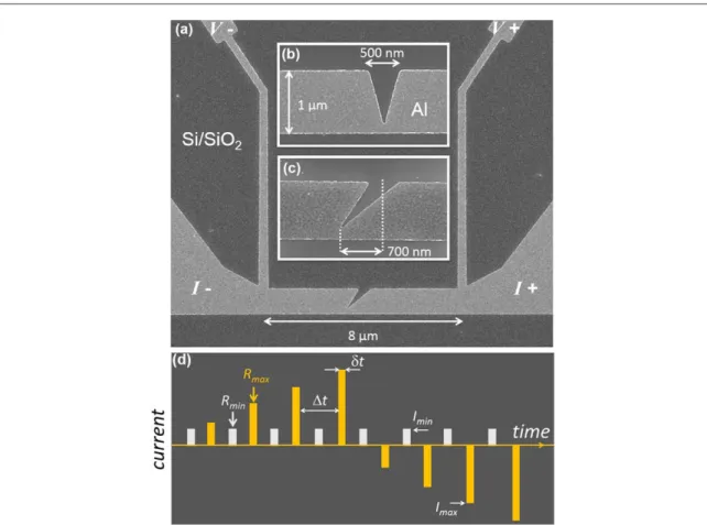
The samples are made of 25 nm thick Alfilms evaporated via electron-beam deposition technique onto a Si wafer with crystallographic orientation(100) and a native oxide layer on top. The wafers are p-doped and have a resistivity of 1.2Ωcm. The Al films are patterned by conventional electron-beam lithography and lift-off procedure using a single 100 nm thick layer of PMMA 950 K resist as a mask. Thefinal layout of the sample is shown infigure1(a) and consists of a 8 μm long and 1 μm wide transport bridge with a border indentantion at
half length. Two types of indentation shapes have been investigated, a symmetric triangular indentation (figure1(b)) and an asymmetric triangular indentation (figure1(c)), both producing a constriction of 200 nm at
the narrowest point along the bridge. SEM images show that the apex of the triangle has a radius smaller than 10 nm and that the Alfilms are polycrystalline with a log-normal grains’ radius distribution maximizing at 20 nm(see supplementary material is available online atstacks.iop.org/NJP/21/113015/mmedia). Several identical samples of each type have been measured. Unless stated otherwise, all measurements are performed in ambient conditions.
2.2. Measurement protocol and criterion for EM breakdown
The samples are electrically excited by a train ofδt=12 ms long pulses and amplitude Imaxstarting at 500μA
and increasing by steps of 200μA (see figure1(d)). These pulses are intercalated by probe pulses Imin=500 μA
delayed by 5 s from the excitation pulse. A resistance Rmaxis measured at the top of the excitation pulse starting
1 ms after the rising edge of the pulse, and a resistance Rminis recorded at the top of the probe pulse. A similar
protocol has been used in[15,33]. At low Imaxvalues, Rmax≈Rmin(see figure2). When Imaxincreases, Rmax
surpasses Rminas a result of Joule heating and afinite resistance temperature coefficient α≈d(ln R)/dT. The
EM current IEMis defined as the point at which the Rminhas changed by 0.25% of its initial value(see figure2(b)).
The train of pulses stops at the moment the increase of Rminhas exceeded 1%. Then, the polarity of the excitation
is inverted, and the same procedure is repeated.
2.3. Estimation of the local temperature at the constriction
Let us have a closer look at the current dependent Rmaxshown infigure2(a). Since a linear increase of resistance of
the device with temperature is observed(see inset in figure2(a)), we can write R(T)=Rbath[1+α(T−Tbath)],
where Rbath=R(Tbath) and Tbathis the temperature of the substrate.
Considering that at the stationary state the total power dissipated, R(T)I2
, is proportional to the induced change of the device average temperature, T−Tbath, we can write R(T)=Rbath(1+γR(T)I2), with γ a factor
Figure 1.(a) Scanning electron microscopy image of the transport bridge with an asymmetric constriction at its center. Zoom in showing the geometrical details of a symmetric(b) and asymmetric (c) constriction. The narrowest point along the bridge (the constriction) is 200 nm wide. (d) Schematic representation of the electrical pump-probe measurements.
Figure 2.(a) Resistance Rmaxmeasured during the current pulse. The solid line corresponds to equation(1) and the solid square symbols are obtained by performingfinite element method simulations using the commercial software COMSOL. Inset: R(T) of the device showing a linear dependence.(b) Resistance Rminmeasured at low current values Imin=500 μA after a current pulse of amplitude Imax. The criterion used to define the onset of electromigration corresponds to a resistance increase of 0.25%, as indicated by the broken line. The indicated temperatures correspond to the maximum value achieved at the constriction just before the probe measurement has been done.
3
depending on the thermal conductivity, specific heat, heat transfer to the substrate and sample geometry as well. From this expression, the following relation can be deduced[19]
g = -( ) ( ) R T R R I 1 . 1 bath bath 2
Infigure2(a) we show Rmaxas a function of current Imaxthrough the device along with thefitting (solid line)
according to equation(1). This theoretical model seems to capture the overall trend of resistance increase due to
Joule heating effects for currents below the onset of EM process(IEM=11.8 mA and current density
JEM=236 MA cm−2). However, it should be noted that the resistance plotted in figure2results from the
electrical potential difference between pads 4μm symmetrically away from the constriction and therefore, for a given applied current I, the temperature distribution is not uniform throughout the bridge. Under this
circumstance, the application of equation(1), which has been deduced under the assumption of uniform
temperature distribution, is uncertain. In order to properly address this problem, it is imperative to resort to numerical simulations of the coupled electric and thermal equations.
We have carried outfinite element method (FEM) simulations using the commercial software COMSOL [42], using as input parameters the experimentally-determined resistance temperature coefficient
α=1.8 × 10³
K−1, the thermal conductivity of the Alfilm [43]k=75 W mK−1, specific heat
[44]C=828 J kgK−1and adjusting the thermal transfer contact with the Si substrate. The FEM simulations confirm the general trend predicted by equation (1) as indicated by the solid square dots in figure2(a). More
details about the FEM simulations are presented in the supplementary material. The FEM simulations allow us to obtain the temperature distribution at the constriction during the current sweep and estimate a local increase of temperature up to∼420 K at the onset of EM. This local temperature will be even higher when the 1% increase of resistance is achieved. Considering that for Al, there is a relief of internal strain(decrease of dislocation density) when the softening temperature ∼450 K is reached, it is expected that even before EM takes place, a change of material properties may occur[45]. Note that Au, previously tested in a monolithic memristive device
[25], has even lower softening temperature (∼390 K) than Al. Although recrystallization and grain growth in Al
will develop at somewhat higher temperatures(∼550 K), it has been shown that nonpassivated Al-1 at.% Si micron size lines under rapid thermal cycling induced by alternating electric current smaller than the EM current, undergo a rapid and significant growth of grains [38].
3. EM-induced resistive switching
3.1. Resistance as control variable
Figure2(b) shows that the resistance of the proposed device can be progressively increased in a fully controllable
fashion. In the case of Al(as for Pt, Au, Pd), the observed resistance increase is typically associated to a combined effect of effective reduction of cross section due to generation of voids at the constriction, and a relief of internal stress, as mentioned above. Note that an increase of resistance of 1% could be obtained by narrowing down the constriction by 15 nm(from 200 to 185 nm) whereas the experimental resistance resolution is about 8 mΩ which can be translated in a width change of about 0.4 nm.
The observed change in the material and geometric properties can, to some extent, be healed by reversing the polarity of the current, thus permitting to recover the initial resistance of the device. In other words, the associated resistive switching produced by the cycle EM/anti-EM on a single metal microstructure uses the resistance of the device as the control variable. Infigure3(a) we demonstrate that this memristive effect can be
reproduced thousands of times. In thisfigure the color code corresponds to the polarity of the bias current. The evolution from low to high resistive state produced by direct EM corresponds to blue color, whereas the passage from high to low resistive state due to anti-EM appears in red.
After an initial training period of about∼30 cycles where the high and low resistive states drift up, the system enters a rather stable phase with high degree of predictibility. These long periods of reproducible switching are occasionally interrupted by a small resistance jump or a change of polarity(see supplementary material). The separation between the inital training and the subsequent stable regime is also seen in the time dependence of the maximum current needed to increase the resistance by 1% as shown infigure3(b) in blue and red for positive
and negative current polarity, respectively. By performing the EM process inside a SEM chamber, we are able to monitor in situ the evolution of the structure. Changes in the structure of the sample can be seen at as early stage as the veryfirst half cycle. Images of the switching process consisting in void generation and void refilling have been reported previously in[24] for Al bow-tie constrictions. In that case a resistance ratio of 250% was used in
order to make more apparent the change in geometry. In the present work we aim for a change of 0.25%(i.e. 1000 times smaller) which may be challenging to capture in a single hysteresis loop. In view of the fact that we are limited in the number of images during in situ inspection before the carbon contamination severely reduces the
contrast, we prioritize the imaging of accumulated damage after several cycles. As expected, the cumulated morphology changes occur in the vicinity of the narrowest point of the structure and take the form of voids. The functionality of a memristor as a two terminal hysteretic switch becomes more evident by combining the data in figures3(a), (b) and plotting δRmin(t)=Rmin(t)−Rmin(0) as a function of current I(t), which is shown in
figure3(c).
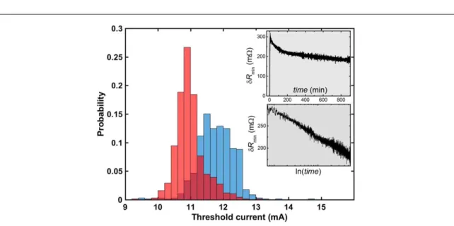
The data infigure3(b) allow us to build up the probability density function (PDF) of the EM current as
shown infigure4. The PDF exhibits a tail at high current values corresponding to the training period, and a sharp peakfingerprint of the more stable switching regime. The distribution in blue color corresponds to the current threshold needed to increase the sample resistance by 0.25%(EM process), whereas in red is the distribution of the threshold current to diminish the resistance by 0.25%(anti-EM process). The fact that the mean value(I ) of the anti-EM current distribution is shifted towards lower current values with respect to the
Figure 3.(a) Temporal evolution of Rminduring 10 d of continuous and uninterrupted switching between low and high resistance state. The inset shows the switching process within a short time interval(∼4 h). The period of the oscillation (i.e. a cycle) is about 20 min.(b) Maximum current needed to increase (blue) or decrease (red) the resistance of the device by 1%. (c) Resistive switching loop obtained by reusing a subset of the data presented in panel(a).
Figure 4. Histogram showing the distributions of threshold currents needed to increase the sample resistance by 0.25%(blue) and decrease it by the same amount(red). The insets show the time relaxation of the high resistance state in linear (upper panel) and logarithmic(lower panel) scales. Here δRmin=Rmin(t)−Rmin(0).
5
EM distribution could be attributed to the fact that the high resistance state corresponds to a narrower constriction and therefore needs a lower current to induce anti-EM. If this is the case, and assuming a constant density of current for EM JEM, we can deduce a change of widthδw≈δI/JEMt∼17 nm, which is in reasonable
agreement with the 15 nm estimated from the increase in resistance.
Alternatively, the difference between the mean values of the distributions shown infigure4, may result from concentration-gradient and stress assisted atom displacement acting in the same direction as the anti-EM current. Indeed, for the anti-EM to heal the sample, there should exist a memory effect guiding the atoms to refill the voids. Under this circumstance, the driving force produced by the gradient of vacancies concentration and stress gradient can lead to a relaxation effect which in turn limits the retention of the device. Previous
investigations of damage relaxation after thermal[46] and electric [47] stress showed a relaxation time on the
scale of days. In[47] it was pointed out that such decay behavior is not purely exponential, but is best described
by a combination of several decay modes. We have performed several tests of the resistance decay after the devices has been set in the high resistance state. The upper inset offigure4shows the relative resistance change δRmin(t) corresponding to the fastest time relaxation that we have found in our devices. The same data is plotted
in the lower inset offigure4with time in log scale, confirming a non exponential decay but rather a logarithmic
decrease. The time lapse needed to reduce the excess resistance at half of its initial value(retention time) can be estimated to∼2 d. A logarithmic relaxation has been reported in a large diversity of physical systems [48] and has
been the subject of significant theoretical work [49]. It is worth mentioning that, a healing process of
electromigrated oxygen vacancies in YBa2Cu3O7−δfilms have shown a stretched-exponential functional
form[50].
3.2. Switching current as control variable
Note that the standard deviation of the probability distribution shown infigure4is rather small, with
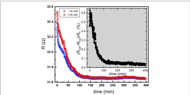
sI I »3%. This fact suggests that the device could be driven by alternative bipolar current pulses offixed amplitude rather than controlling the actual resistance of the device. In order to test this hypothesis, we submit a sample to high current pulses of I=±14 mA for ‘write-state’, intercalated with low current amplitude pulse I=0.5 mA for ‘read-state’. Prior to these measurements, the initial value of the EM current was precisely defined following the procedure illustrated in figure2. A clear advantage of this method with respect to the approach discussed in the previous section is the abillity to change the state with a single pulse and therefore reach higher toggle frequencies. Unfortunately, the representative results shown infigure5indicate a discouraging decrease of the separation between the high and low resistance state as a function of time. The reason for this behavior likely arises from the fact that the same pulse amplitude for the two opposite polarities has been used, even though the probability distribution shown infigure4indicates that the current needed for EM and that required for anti-EM differ by aboutδ I=1 mA. An initial training period of about 300 cycles is also observed in this case. Figure6(a) shows a SEM image of the damage produced at the constriction after 2500
cycles.
Figure 5. Time evolution of the high and low resistance states as read by a small current pulse after alternating writing pulses of constant amplitude±14 mA. The inset show the percentage change of resistance between the high and low resistance states normalized by the initial resistance of the device.
3.3. Asymmetric structures
In 1998 Derenyi et al[51] theoretically predicted that the application of AC electric fields could favor the
smoothing process during annealing thanks to a ratchet effect of surface EM. Some experimental evidence supporting this scenario was soon after shown by de Pablo et al[52] through scanning force microscopy in gold
micro-stripes. More recently, lateral asymmetries in the nanostructures have shown to also produce an
asymmetric EM current[53,54] chiefly due to the resulting asymmetric temperature distribution. Motivated by
these works we have compared the polarity dependence of the EM current for symmetric and asymmetric structures(see figures1(b) and (c)), although we were unable to find a clear trend since the dispersion from one
sample to another was more important that the differences observed between symmetric and asymmetric structures.
According to Black’s law, the lifetime of the device is proportional to J−2and depends exponentially on T−1.
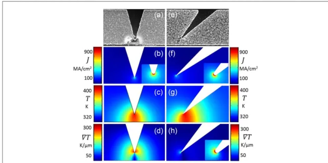
In addition, if important temperature gradients develop, thermomigration(TM) may compete or reinforce the EM process. Figure6shows FEM of the temperature distribution, temperature gradient and current crowding for the symmetric(b)–(d) and asymmetric (f)–(h) constrictions for I=10 mA. Although the current density seems to be rather insensitive to the symmetry of the constriction, the temperature landscape exhibits a clear asymmetry that could favor EM ratchet effect if TM would play an important role. The fact that we have not observed a clear ratchet signal seems to indicate that TM does not play a dominant role in our structures.
It would require a colossal experimental effort to quantify the relative importance of each mechanism due to the fact that EM, stress migration(SM), and TM are tightly interlinked. Indeed, current density increases the temperature through Joule heating and in turn, the temperature rise influences mechanical stress through differences in the expansion coefficients. In other words, the particular damage observed in the investigated sample(figure7) cannot be attributed to a given migration type since all diffusion processes eventually lead to
voids. There are, however, some indications concerning the location of the damage which could provide certain clues about the dominant mechanism at play.
Notefirst that for a symmetric structure, TM would lead to symmetric distribution of damage. In contrast to that, EM is driven by current and therefore the induced damage may not necessarily respect the symmetry of the structure as indeed observed. In addition, EM damage is most likely to be found in areas of high current density (current crowding effect) whereas the maximum temperature gradient should occur at about a thermal healing length(Δ) distance from that point. We estimate Δ∼0.5 μm in our sample. The fact that the first voids are seen exactly at the constriction seem to reinforce the idea that TM is less relevant than EM. Furthermore, it is believed that hillocks, as the ones observed in our samples, usually result from EM rather than TM.
The role of SM is more delicate to evaluate since SM is driven by mechanical stress which may be pre-existing due to deposition of Al onto SiO2. As temperature rises during EM, the huge difference(a factor of about 50) in
thermal expansion coefficients of the metal and the insulator can result in substantial tensile stress. Even in absence of the above effects, EM will produce dislocation of metal atoms inducing mechanical stress and hence SM. The resulting SM acts in the opposite direction than EMflow and the damaging dislocation due to EM will
Figure 6. Scanning electron microscopy images of the symmetric(a) and asymmetric (e) devices after several thousand switching cycles. The inhomogeneous current density distributions and the corresponding current crowding effects at the constrictions are shown in panels(b) and (f). The temperature distributions are shown in panels (c) and (g), whereas the temperature gradients, relevant for thermomigration effects, are depicted in panels(d) and (h).
7
be slowed down. A close inspection to the series of in situ images of an asymmetric device under EM/anti-EM cycles presented infigure7reveals the creation of voids along a border where neither current density nor temperature gradients are important. This observation leads us to conclude that SM should be invoked to understand the atomic migration in these memristive devices.
4. Conclusion
We have investigated the performance of monolithic metallic microwires with an indentation, as candidates for two-terminals resistance switching(memristors) induced by current-stimulated atomic migration. The controllability and reproducibility of the low-amplitude switching process between high and low resistance states has been tested during 103cycles with a retention that is, at worst, of few days. The inconvenience of controlled resistance switching is the involved procedure and the consequent slowness. An attempt for faster switching withfixed current amplitude of alternating polarity, showed a poor performance in terms of stability and reproducibility. The fastest operation frequency is limited by the heat dissipation time constant of about 10 ns as estimated from FEM. For resistance values of∼35Ω and current amplitudes ∼15 mA, the power dissipated to switch the resistance from low to high(or viceversa) is P=RI2∼8 mW. Assuming that this switching can be achieved with a 10 ns pulse(lower bound imposed by the thermal evacuation time), the energy per bit amounts to 80 pJ. This is to compare with other memory devices as in[28]. For instance, USB flash drives
allow reading, writing, and erasing of data, with endurance of 1 million write/erase cycles in each cell of memory. Although the concept of a memristive device based on EM seems to be viable, in order to comply with the milestones already set by competing alternative approaches, devices should be considerably scaled down. By doing so, based on geometrical considerations, one is led to conclude that less current will be needed to induce resistance switching and consequently less power consumption will be associated to this process. However, as dimension shrinks the heat evacuation towards the substrate improves and lower temperatures are achieved. Since EM is a thermally activated process, this means that the threshold current for triggering EM will not simply scale with the width of the constriction. EM at lower temperatures is highly desirable since other effects than material transport, such as crystallization or alloying, are reduced and thus healing effects obtained by reversing the current polarity may become more reversible. This would open the possibility to explore higher melting-point materials such as Cu. As an extra benefit of low dimensional devices we should mention the substantial Figure 7. Sequence of scanning electron microscopy images of an asymmetric device during the alternating switching process. The time separation between two consecutive images corresponds to about 15 cycles high resistance-low resistance. Panel(a) shows the sample in the virgin state. In panel(b), an elongated void at the tip of the constriction is visible. In panel (c) an overgrowth of material develops at the constriction and a void appears in the internal side of the triangular constriction, where the current density is particularly weak. At later stages(d)–(h) the overgrowth increase in size at the same time that other voids develop along the lower border of the sample. The fact that the location of the voids do not coincide with the points of maximum temperature, gradient of temperature, or current density, indicates that SM is at play. The width of the bridge is 1μm.
increase of the on-to-off ratio facilitating the reading process. As a last note, if the constriction width was smaller than the mean grain size(∼20–30 nm) the dynamics of the EM is expected to change due to the bamboo-like structure.
Acknowledgments
The authors thank the Fonds de la Recherche Scientifique—FNRS. J Lombardo acknowledges support from FRS-FNRS(FRIA Research Fellowship). The work of AVS has been partially supported by the grant CDR J.0151.19 of the FRS-FNRS. The work of NDN has been partially supported by the grant CDR J.0124.19 of the FRS-FNRS. The authors thank the ULiege Microscopy facility CAREM for the AFM and SEM investigations.
ORCID iDs
J Lombardo https://orcid.org/0000-0002-5993-2123
N D Nguyen https://orcid.org/0000-0002-0142-1611
A V Silhanek https://orcid.org/0000-0001-9551-5717
References
[1] Loyd J R 1997 Electromigration in thin film conductors Semicond. Sci. Technol.12 1177
[2] Esen G and Fuhrer M S 2005 Temperature control of electromigration to form gold nanogap junctions Appl. Phys. Lett.87 263101
[3] Strachan D R, Smith D E, Johnston D E, Park T-H, Therien M J, Bonnell D A and Johnson A T 2005 Controlled fabrication of nanogaps in ambient environment for molecular electronics Appl. Phys. Lett.86 043109
[4] Trouwborst M L, van der Molen S J and van Wees B J 2006 The role of Joule heating in the formation of nanogaps by electromigration J. Appl. Phys.99 114316
[5] Ittah N, Yutsis I and Selzer Y 2008 Fabrication of highly stable configurable metal quantum point contacts Nano Lett.8 922
[6] Campbell J M and Knobel R G 2013 Feedback-controlled electromigration for the fabrication of point contacts Appl. Phys. Lett.102 023105
[7] Baumans X D A et al 2016 Thermal and quantum depletion of superconductivity in narrow junctions created by controlled electromigration Nat. Commun.7 10560
[8] Lombardo J, Jelic Z L, Baumans X D A, Scheerder J E, Nacenta J P, Moshchalkov V V, Van de Vondel J, Kramer R B G, Milosevic M V and Silhanek A V 2018 In situ tailoring of superconducting junctions via electro-annealing Nanoscale10 1987
[9] Robbes D, Miklich A H and Kingston J J 1990 Josephson weak links in thin films of YBa2Cu3O7−xinduced by electrical pulses Appl. Phys. Lett.56 2240
[10] Keijers W, Baumans X D A, Panghotra R, Lombardo J, Zharinov V S, Kramer R B G, Silhanek A V and Van de Vondel J 2018 Nano-SQUIDs with controllable weak links created via current-induced atom migration Nanoscale10 21475
[11] Blanco Alvarez S, Brisbois J, Melinte S, Kramer R B G and Silhanek A V 2019 Statistics of thermomagnetic breakdown in Nb superconductingfilms Sci. Rep.9 3659
[12] Gurunarayanan S P, Verellen N, Zharinov V S, Shirley F J, Moshchalkov V V, Heyns M, Van de Vondel J, Radu I P and Van Dorpe P 2017 Electrically driven unidirectional optical nanoantennas Nano Lett.17 7433
[13] Sannicolo T et al 2016 Direct imaging of the onset of electrical conduction in silver nanowire networks by infrared thermography: evidence of geometrical quantized percolation Nano Lett.16 7046
[14] Bellet D et al 2017 Transparent electrodes based on silver nanowire networks: from physical considerations towards device integration Materials10 570
[15] Wu Z M, Steinacher M, Huber R, Calame M, van der Molen S J and Schonenberger C 2007 Feedback controlled electromigration in four-terminal nanojunctions Appl. Phys. Lett.91 053118
[16] Kanamaru Y, Ando M and Shirakashi J-I 2015 Ultrafast feedback-controlled electromigration using a field-programmable gate array J. Vac Sci. Technol. B33 02B106
[17] Heersche H B, Lientschnig G, O’Neill K, Van Der Zant H S J and Zandbergen H W 2007 In situ imaging of electromigration-induced nanogap formation by transmission electron microscopy Appl. Phys. Lett.91 072107
[18] Talukder S, Ghosh A and Pratap R 2012 Nanoscale control of electro-migration for resistance tuning of metal lines J. ISSS 1 16 [19] Zharinov V S, Baumans X D A, Silhanek A V, Janssens E and Van de Vondel J 2018 Controlled electromigration protocol revised Rev.
Sci. Instrum.89 043904
[20] Xiang C, Kim J Y and Penner R M 2009 Reconnectable sub 5 nm nanogaps in ultralong gold nanowires Nano Lett.9 2133
[21] Li Z, Bauer C L, Mahajan S and Milnes A G 1992 Degradation and subsequent healing by electromigration in Al-1 wt Si thin films J. Appl. Phys.72 1821
[22] Hong C-F, Togo M and Hoh K 1993 Repair of electromigration-induced voids in aluminum interconnection by current reversal Japan. J. Appl. Phys.32 L624
[23] Kozlova T, Rudneva M and Zandbergen H W 2003 In situ TEM and STEM studies of reversible electromigration in thin palladium-platinum bridges Nanotechnology24 505708
[24] Baumans X D A et al 2017 Healing effect of controlled anti-electromigration on conventional and high-Tc superconducting nanowires Small13 1700384
[25] Johnson S L, Sundararajan A, Hunley D P and Strachan D R 2010 Memristive switching of single-component metallic nanowires Nanotechnology21 125204
[26] Chua L O 1971 Memristor-the missing circuit element IEEE Trans. Circuit TheoryCT-18 507
Chua L O and Kang S M 1976 Proc. IEEE64 209
Prodromakis T, Toumazou C and Chua L O 2012 Nat. Mater.11 478
9
[27] Strukov D B, Snider G S, Stewart D R and Williams R S 2008 The missing memristor found Nature453 80
[28] Yang J J, Strukov D B and Stewart D R 2013 Memristive devices for computing Nat. Nanotechnol.8 13
[29] Naitoh Y, Horikawa M, Abe H and Shimizu T 2006 Resistance switch employing a simple metal nanogap junction Nanotechnology
17 5669
[30] Schirm C, Matt M, Pauly F, Cuevas J C, Nielaba P and Scheer E 2013 A current-driven single-atom memory Nat. Nanotechnol.8 645
[31] Minnai Ch, Bellacicca A, Brown S A and Milani P 2017 Facile fabrication of complex networks of memristive devices Sci. Rep.7 7955
[32] Palau A et al 2018 Electrochemical tuning of metal insulator transition and nonvolatile resistive switching in superconducting films ACS Appl. Mater. Interfaces10 30522
[33] Baumans X D A, Fernández-Rodríguez A, Mestres N, Collienne S, Van de Vondel J, Palau A and Silhanek A V 2019 Electromigration in the dissipative state of high-temperature superconducting bridges Appl. Phys. Lett.114 012601
[34] Maan A K, Jayadevi D A and James A P 2017 A survey of memristive threshold logic circuits IEEE Trans Neural Netw. Learn. Syst.
28 1734
[35] Zidan M A, Chen A, Indiveri G and Lu W D 2018 Memristive computing devices and applications Nat. Electron.1 22
[36] Moenig R, Park Y B and Volkert C A 2006 Thermal fatigue in copper interconnects AIP Conf. Proc.817 147
[37] Park Y-B, Moenig R and Volkert C A 2007 Frequency effect on thermal fatigue damage in Cu interconnects Thin Solid Films515 3253
[38] Keller R R, Geiss R H, Barbosa N, Slifka A J and Read D T 2007 Strain-induced grain growth during rapid thermal cycling of aluminum interconnects Metall. Mater. Trans.38A 2263
[39] Luo X M, Zhang B and Zhang G P 2014 Frequency-dependent failure mechanisms of nanocrystalline gold interconnect lines under general alternating current J. Appl. Phys.116 103509
[40] Moenig R, Keller R R and Volkert C A 2004 Thermal fatigue testing of thin metal films Rev. Sci. Instrum.75 4997
[41] Wang M, Zhang B, Zhang G P and Liu C S 2011 Scaling of reliability of gold interconnect lines subjected to alternating current Appl. Phys. Lett.99 011910
[42] COMSOL Multiphysics 2015 Joule Heating Modulewww.comsol.com(Stockholm, Sweden: COMSOLAB)
[43] Avery A D, Mason S J, Bassett D, Wesenberg D and Zink B L 2015 Thermal and electrical conductivity of approximately 100-nm permalloy, Ni, Co, Al, and Cufilms and examination of the Wiedemann–Franz law Phys. Rev. B92 214410
[44] Song Q, Cui Z, Xia S and Chen S 2004 An ac microcalorimeter for measuring specific heat of thin films Microelectron. J.35 817
[45] Holm R 1967 Electric Contacts: Theory and Application (Berlin: Springer) (https://doi.org/10.1007/978-3-662-06688-1)
[46] Hershkovitz M, Blech I A and Komem Y 1985 Stress relaxation in thin aluminium films Thin Solid Films130 87
[47] Lloyd J R and Koch R H 1988 Study of electromigrationinduced resistance and resistance decay in Al thin film conductors Appl. Phys. Lett.52 194
Ringler I J and Lloyd J R 2016 Stress relaxation in pulsed DC electromigration measurements AIP Adv.6 095118
[48] Rossel C, Maeno Y and Morgenstern I 1989 Phys. Rev. Lett.62 681
Amir A, Oreg Y and Imry Y 2010 Annu. Rev. Condens. Matter Phys.2 235
Amir A, Oreg Y and Imry Y 2008 Phys. Rev. B77 165207
Lahini Y, Gottesman O, Amir A and Rubinstein S M 2017 Phys. Rev. Lett.118 085501
Matan K, Williams R B, Witten T A and Nagel S R 2002 Phys. Rev. Lett.88 076101
[49] Amir A, Oreg Y and Imry Y 2011 Proc. Natl Acad. Sci. USA109 1850
Balankin A S, Huerta O S, Mendez F H and Ortiz J P 2011 Phys. Rev. E84 021118
Cugliandolo L F, Kurchan J and Ritort F 1994 Phys. Rev. B49 6331
Sibani P and Hoffmann K H 1989 Phys. Rev. Lett.63 2853
Pleimling M and Tauber U C 2011 Phys. Rev. B84 174509
Du X, Li G, Andrei E Y, Greenblatt M and Shuk P 2007 Nat. Phys.3 111
Cugliandolo L F and Kurchan J 1993 Phys. Rev. Lett.71 173
Amir A, Oreg Y and Imry Y 2009 Phys. Rev. Lett.103 126403
[50] Moeckly B H, Lathrop D K and Buhrman R A 1993 Electromigration study of oxygen disorder and grain-boundary effects in YBa2Cu3O7−δthinfilms Phys. Rev. B47 400
[51] Derenyi I, Lee C and Barabási A-L 1998 Ratchet effect in surface electromigration: smoothing surfaces by an ac field Phys. Rev. Lett.
80 1473
[52] de Pablo P J, Colchero J, Gomez-Herrero J, Asenjo A, Luna M, Serena P A and Baro A M 2000 Ratchet effect in surface electromigration detected with scanning force microscopy in gold micro-stripes Surf. Sci.464 123
[53] Tian H, Ahn W, Maize K, Si M, Ye P, Alam M A, Shakouri A and Bermel P 2018 Thermoreflectance imaging of electromigration evolution in asymmetric aluminum constrictions J. Appl. Phys.123 035107
[54] Sawtelle S D, Kobos Z A and Reed M A 2019 Critical temperature in feedback-controlled electromigration of gold nanostructures Nanotechnology30 015201