HAL Id: hal-01622569
https://hal.archives-ouvertes.fr/hal-01622569
Submitted on 9 Mar 2020
HAL is a multi-disciplinary open access
archive for the deposit and dissemination of
sci-entific research documents, whether they are
pub-lished or not. The documents may come from
teaching and research institutions in France or
abroad, or from public or private research centers.
L’archive ouverte pluridisciplinaire HAL, est
destinée au dépôt et à la diffusion de documents
scientifiques de niveau recherche, publiés ou non,
émanant des établissements d’enseignement et de
recherche français ou étrangers, des laboratoires
publics ou privés.
Embedded spectroscopic reflectometry metrology on
FEOL silicon dioxide trench polishing equipment: ER:
Equipement reliability and productivity enhancements
Sophia Bourzgui, Agnès Roussy, Jakey Blue, Gaëlle Georges, Emilie Faivre,
Karen Labory, Jacques Pinaton
To cite this version:
Sophia Bourzgui, Agnès Roussy, Jakey Blue, Gaëlle Georges, Emilie Faivre, et al..
Embedded
spectroscopic reflectometry metrology on FEOL silicon dioxide trench polishing equipment: ER:
Equipement reliability and productivity enhancements. Advanced Semiconductor Manufacturing
Con-ference (ASMC 2017 ), May 2017, Saratoga Springs, United States. �10.1109/ASMC.2017.7969267�.
�hal-01622569�
Embedded Spectroscopic Reflectometry Metrology on
FEOL Silicon Dioxide Trench Polishing Equipment
ER: Equipement Reliability and Productivity Enhancements
S. Bourzgui
1,2,3,a, A. Roussy
1, J. Blue
1, G. Georges
2, E. Faivre
3, K. Labory
3and J. Pinaton
31 Mines Saint-Etienne and LIMOS, UMR CNRS 6158, CMP Georges Charpak, F-13541 Gardanne, France 2Aix-Marseille Université, CNRS, Centrale Marseille, Institut Fresnel UMR Marseille, France
3STMicroelectronics, Rousset, France ae-mail: sophia.bourzgui@st.com
Abstract—The challenge in the research is to develop a material thickness measurement method to monitor oxide polishing by
Chemical-Mechanical Planarization (CMP) in the Shallow Trench Isolation (STI). The underlying aim is to build a statistical regulation model for the polishing time on one platen (the two others platens are monitored by an endpoint signal). In addition to the process parameters (head sweep, platen, and head rotation velocity), input and output polished material thicknesses data are essential to build a run-to-run model for CMP. Therefore, stack layer thickness, before and after polishing, needs to be measured fast enough to maintain the acceptable throughput and to control truthfully the polishing time wafer by wafer.
In this paper, we describe how the spectroscopic reflectometry embedded in the polishing equipment, can meet the requirements of rapidity and capability of setting up a run-to-run control algorithm to maintain the thickness target for CMP STI.
Keywords—metrology model; spectroscopic reflectometry; multilayer thickness measurement; Shallow Trench Isolation (STI);
Chemical-Mechanical Planarization (CMP) process.
I. INTRODUCTION
During the semiconductor device process flow, a thin deposition of silicon dioxide (SiO2) fills up isolation trenches to electrically separate doped silicon active areas where transistors will be implemented. The STI CMP role is to erase the remaining surface topology and clear SiO2 over the active areas. To carry out this step, a Si3N4 material under SiO2 deposition is used as a stop layer and is removed after CMP. The polishing is finalized by clearing the Si3N4 surface, removing the entire SiO2 layer, and then the Si3N4 is slightly polished, too. As a consequence, the STI CMP process is controlled by two outputs:
• A delta Si3N4 which represents the thin Si3N4 layer removed • SiO2 thickness from the isolation trench
In this study, a metrology strategy to control the process is set up and spectroscopic reflectometry models are developed for dielectric layer measurements, which are correlated with the film stacks before and after SiO2 trench polishing. To validate the model, our approach is firstly to test the repeatability and reproducibility of metrology models by decomposing the variance components with the ANOVA (Analysis Of Variance) method. On the other hand, reflectometry models are tested in extreme case conditions in order to prove that the CMP process issues can be still caught. Finally, a double data collection on patterned wafers illustrates the well-matched thickness results between the reflectometry models and ellipsometry models used on the production line.
This paper investigates the feasibility of measuring the STI CMP thickness by spectroscopic reflectometry in a production context on 90nm node. These preliminary works give promising results of reproducibility and potential for setting up a mathematical model to determine the precise volume of SiO2 thickness to be removed using input and output material thickness data.
II. SPECTROSCOPIC REFLECTOMETRY MEASUREMENT FOR PRODUCTION A. Spectroscopic Reflectometry Principle
This optical technique is widely used in the semiconductor industry to calculate semi-transparent film thickness, mono or multilayers stacks. The light effect used here is based on interferometry principle. Thanks to a specific configuration, the light beams reflected by each layer interface overlap and can, under particular assumptions (spatial and temporal coherences), create
interferences. Those could be constructive or destructive interferences depending on the wavelength, thickness layers and refractive indeces of the materials. The light reflected by the sample measured can be described as a function of the wavelength. The spectroscopic reflectometer Nano9000i has a halogen source with a white light spectrum (400-800nm) and a spot size of 17µm. As is shown in Fig. 1, for one sample, we obtain the reflectance over a spectrum of wavelengths, the former being the ratio between the intensity of reflected light on the sample and the incident beam intensity, for each wavelength. To extract the sample layer thicknesses, the sample spectrum is compared to a theoretical spectrum determined by a film stack model. For each layer of the stack, a thickness target is set and the Goodness of Fit (GOF) from 0 to 1 enables to estimate the level of confidence of sample thickness results compared to the target. The GOF is related to the difference between the theoretical signal of the model and the signal of the measured data, called the residual. A GOF close to 1 signifies a perfect correlation between the sample spectrum and the model spectrum, which means a residual close to 0. To determine material thicknesses in spectroscopic reflectometry, material optical properties have to be known and can be determined by spectroscopic ellipsometry.
Fig. 1. The spectrum of the Reflectance (%) in function of the Wavelength (nm) illustrates the overlap of the theoretical model (red line) and measured sample (green line) with an GOF average of 99% for the two measured data. Here the film stack measured is before the STI process: SiO2/ Si3N4/SiO2/Si
B. Metrology Strategy for SiO2 Trench Polishing Control
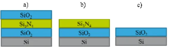
CMP is essential to create a material surface as smooth as possible to enable the photolithography process to evnly focus across the wafer surface. To design STI, trenches are etched in the Si substrate, filled up by a thick SiO2 layer, and then the surface is planarized by CMP. To monitor the STI CMP process, a silicon nitride (Si3N4) layer is deposited by Chemical Vapor Deposition (CVD) and used as a stopping layer, above a thin SiO2 film called “pad oxide”. To recap, three different film stacks exist on the wafer at the STI CMP step (see Fig. 2):
Film stack 1: SiO2/Si3N4/SiO2/Si (cf. Fig. 2a) • SiO2: active zone isolation
• Si3N4: stop layer for STI CMP
• SiO2: called “pad oxide” to protect active zone • Si: substrate
Film stack 2: Si3N4/SiO2/Si (cf. Fig. 2b) • Si3N4: stop layer for STI CMP
• SiO2: called “pad oxide” to protect active zone • Si: substrate
Film stack 3: SiO2/Si (cf. Fig. 2c) • SiO2: active zone isolation • Si: substrate
Fig. 2. Schematic representation of film stacks before the STI polishing step shown by a) where the SiO2 layer covers entirely the wafer surface and after polishing shown by b) and c) where the SiO2 is removed from the Si3N4 surface and situated only in trenches for the purpose of electrically isolating the active zones.
The aim of the Si3N4 and SiO2 thicknesses measures before and after polishing is twofold:
On one hand, we want to be sure that there is no SiO2 residue remaining on the Si3N4 layer. SiO2 residues can lead to etching lag during the Si3N4 removal step and consequently leave Si3N4 residues on the wafer, which is a killer defect. To avoid residual SiO2 on Si3N4 surface, Si3N4 layer is slightly polished (about 6nm).
On the other hand, we want to control the SiO2 trench depth to catch over-polishing or a singular issue in the CMP process, known as “dishing issue” in the SiO2 trenches, i.e. the latter being too shallow, potentially leading to shorting between consecutive transistors.
Two key parameters validate the polishing process: the thickness of the removed Si3N4 layer, which guarantees the step height defined by designers for each product after Si3N4 chemical removal and the thickness of the SiO2 isolation trench, which must be sufficient to avoid shortcuts between transistors.
To reach our goal, we have to take into account spectroscopic reflectometry modeling limitations in determining the dielectric material thicknesses. The film thickness measurement capability for the NanoSpec 9000 thin film measurement system used ranges from 25nm to 25µm. The Si3N4 layer thickness (about 110nm) and the SiO2 layer thickness for the isolation trench (about 450 to 600nm), are within the film thickness range and can be determined with a GOF close to 1. However, if we consider the 7nm of the SiO2 pad oxide, we are far below the measurement capability of the tool and thus have to assume this thickness is a constant in our model. To actually determine the value of thus constant, we use an ellipsometer to verify the pad oxide growth post measurement. By looking at over a year of pad oxide thickness measures, we were able to conclude that the data are stable and have a small dispersion of about 0.6nm. It is small enough to set the SiO2 pad oxide thickness at a fixed value in our pre and post CMP model, with little to no impact on the accuracy of the other Si3N4 and SiO2 measured thicknesses.
Furthermore, according to the principles of reflectometry, the obtained spectrum will depend on the intensity of the light beam received by the receptor. Hence, thicknesses and GOF are dependent on the halogen light source calibration (done with a known reference sample) and lamp life time, which determines the signal intensity of incident beam.
Finally, we were able to demonstrate that recipe robustness is essential to avoid mechanical precision drifts over time, resulting in out of control GOF limits for the measured film stack. While the rapidity of the measure is a key parameter in order to have a correct wafer throughput, we had to establish a camera based image recognition process for each measurement sites to compensate for the mechanical displacement between each sites of one wafer. This resulted in a slight throughput overhead.
C. Building a film strategy model:
To build a film strategy, it is necessary to have a sample as a reference and make a measure with the spectroscopic reflectometer to generate experimental data. With the spectrum associated to these experimental data, the model construction is set up using a film strategy software like the ADAP (Advanced Data Acquisition Package) program interface, of the N2000i software. In the model, each layer has its own material file in the film stack model with specific characteristics (thickness target, thickness range, type of film material).
TABLE I. MEASUREMENT PARAMETERS CHOSEN FOR THE SPECTROSCOPIC REFLECTOMETRY PRE AND POST-MODELS TO CONTROL THE SIO2 AND SI3N4 THICKNESSES BEFORE AND AFTER STI CMP
Before STI CMP After STI CMP
Number of layers: 4 2 3
Material type for each layer: SiO2: Cauchy Si3N4: Cauchy SiO2 : constant SiO2: Cauchy Si: substrate Si3N4: Cauchy SiO2: constant Si: substrate
Si: substrate Target thickness (nm): 600/110/7/Si substrate 450/Si substrate 100/7/Si substrate Range of thickness for film (nm): SiO2 600 ± 200 450 ± 150 100 ± 50 Si3N4 110 ± 50 7 (constant) SiO2 7 (constant)
To determine the Si3N4 layer pre- and post-thickness and the SiO2 trench depth, we use a Cauchy model as shown below depending on the wavelength, where optical properties are defined by the equations:
3 2 λ λ C B A n= + + , and (1) 5 3 λ λ λ G F E k= + + , (2) where n is the refractive index and k indicates the absorption coefficient. The parameters A to G are determined with reference sample.
In the visible light spectrum, the absorption coefficient k is close to 0 for the two semi-transparent material Si3N4 and SiO2 and the refractive index varies from 1.47 to 1.45 for SiO2 and ranges from 2.10 to 2.02 for the Si3N4. [1]
As mentioned previously, thin pad oxide thickness is outside the reflectometers measuring range (250 angstroms - 25 microns). We will consider that the process deposition of buried oxide is stable and has a small dispersion of about 0.6nm. This assumption provides a good approximation of the pad oxide thickness. Furthermore, since the ellipsometry model used in production already has a set value for this layer thickness, we are able to maintain a good correlation between the two models.
The aforementioned production model also integrated an upper layer of Si3N4. As ellipsometry uses light polarization properties to determine layer thickness [2], slurry particles and mechanical pressure on the surface of the material increase its roughness and can cause disturbance in the measure of the Si3N4 layer. However our spectroscopic reflectometry model uses light interferometry properties on thin film materials and post CMP roughness of Si3N4 (under 0.1nm) will not impact it. This is why an upper layer Si3N4 model is not needed.
Initially, repeatability and reproducibility (R&R) tests were accomplished to validate the 3 models and the measure equipment.
III. PRELIMINARY TESTS A. Repeatability and Reproductibility Tests
In order to evaluate measurement variations relative to the environment, the equipment, and the model, we perform an ANOVA with the standard deviation of the measurement system expressed as:
100 & & % = × TV R R R R , (3) ² ² &R PV R TV = + , (4) 100 % = × TV PV PV , (5) %Repeatability =% = ×100 TV EV EV (6) %Reproducibility =% = ×100 TV AV AV (7)
PV: Part Variation (measurement sites) EV: Equipment Variation
AV: Appraiser Variation
The equipment capability depending on the range of specifications limits is expressed as: Capability Process Measurement: CPM = ((USL – LSL)/R&R) with USL (Upper Specification Limits) and LSL (Lower Specification Limits) [6].
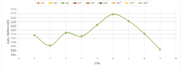
The reflectometry models are experimented on a patterned wafer. Three successive measures are done to test the repeatability and repeated during three successive days to study the reproducibility (see Fig. 3). The level of confidence is set to 0.99%.
Fig. 3. The test is made on the nine sites of one wafer, with three consecutive measures, repeated for three days, on one unique reflectometer. The nine trends represent the raw data of Si3N4 thickness before polishing (vertical axis) in function of the measurement site (horizontal axis).
In order to pass the acceptance criteria, values have to be lower than 10% for %R&R and greater than 10 for the CPM criteria. As is shown in Table II, values measured for Si3N4 and SiO2 layer thicknesses before and after polishing pass the process control criteria.
TABLE II.FROM THE RAW DATA OF SI3N4 AND SIO2 THICKNESSES BEFORE AND AFTER POLISHING, WE CALCULATED THE R&R AND THE CPM DEPENDING OF THE RANGE SPECIFICATION LIMITS, SPECIFIC FOR EACH LAYER.
Si3N4 Pre SiO2 Pre Si3N4 Post SiO2 Post %R&R < 10% 3.13% 0.45% 0.76 % 1.01%
CPM > 10 22.15 158.07 192.71 63.48
Since the models need to be repeatable and reproducible, we need to demonstrate that they catch STI CMP process issues such as under and over polishing and signal them properly.
B. Corner Tests
To qualify a new metrology model, we have to validate if the metrology detects the process or equipment issues and gives relevant information of the issues. In the CMP process, two atypical situations can happen: under-polishing with the risk of having residual SiO2 on active areas and over-polishing which can create shortcut due to an insufficient step height.
Over-polishing is well detected by spectroscopic reflectometry models. Indeed, if too much Si3N4 has been removed and there is no SiO2 residue such that the post-polishing model of Si3N4/SiO2/Si is not disturbed.
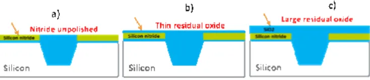
However, under-polishing has to be tested to validate that the model catches a potential oxide residue on top of the Si3N4 layer. Consequently, we created three under polishing scenarii (Fig. 4), and measured them with the two approaches: ellipsometry and reflectometry:
a) The wafer process is stopped before being polished on the third platen, which is the function of the roughness surface reducing and is the one that actively consumes the Si3N4 layer
b) In this case, the process is interrupted on platen 2, which a remaining SiO2 layer on top of the Si3N4 surface of a thickness under 25nm. The SiO2 layer is under the lower reflectometry measure limit.
c) The wafer process is interrupted after being polished on platen 1, which leaves a large SiO2 layer of about 100nm above the Si3N4 surface.
Fig. 4. Schematic representation of a three transverse views of under-polishing conditions for STI CMP process.
For the first configuration (cf. Fig. 4(a)), nine sites of the wafer are measured under reflectometry and ellipsometry method. We notice in both case that the Si3N4 layer has been slightly abraded on the center of the wafer, represented by the site number 9 on Fig. 5, which has a greater than 0 measurement. On the other sites, the measurements of Si3N4 thickness are under the LSL (Low Specification Limit), close to 0, i.e., according to the reflectometry model, the Si3N4 layer remains unpolished.
Fig. 5. This graph refers to the a) condition of under-polishing. The two curves are measured on the nine sites of one wafer, by reflectometry and ellipsometry methods, and show the removed Si3N4 thickness.
Scenario b) is the most critical one because the residual SiO2 layer thickness is below the reflectometer detection capability. It means that as far as the reflectometry model is concerned there might as well not be any residual SiO2. However it is still possible to detect the issue because that residual layer thickness will be added to the Si3N4 layer measure, thus indicating a negative delta of thickness removed which is a physical non-sense (see Fig. 6).
Fig. 6. Si3N4 removed thickness (vertical axis) measured by reflectometry on the nine sites of one wafer (horizontal axis) where the residual SiO2 thickness is under the window reflectometer detection (refers to the Fig. 3(b)).
Finally, scenario c) is caught with the Si3N4/SiO2/Si reflectometry model by looking at the GOF control chart, which is generally under 99%, (the lower control limit to confirm the measure confidence) which means that the obtain Si3N4 thickness data are aberrant.
In the following section, a matching analysis of reflectometry metrology with the reference equipment is implemented in order to validate the proposition of this research.
IV. DOUBLE DATA COLLECTION FOR VALIDATION ANALYSIS
Double data collection is realized on 26 wafers from random lots with the same pre and post metrology recipes for one product on one Nano9000i reflectometer from Nanometrics and one ASETF5 ellipsometer from KLA TENCOR.
A. SiO2 thickness in isolation trench
The double data collection shows a maximum mismatch of 1.5nm between the reflectometer and the ellipsometer. That represents a difference less than 0.30% of measured values, what is under the 1% upper limit of authorized mismatch setting by the metrology process control.
Fig. 7. Double data collection on twenty-six wafers from random lots of one products (horizontal axis). Shown above is the SiO2 trench thickness average (vertical axis) after polishing. The average is made on nine measurement sites on a single wafer with the maximum and the minimum value also being presented for each average.
The weak mismatch of SiO2 thickness shown in Fig. 7 can be explained by the correlation between the CMP process outcome and the different spot sizes of both tools incident beams. As previously stated one of the most paramount CMP process problematics is the apparition of a “dishing issue” in low density zones without pattern. SiO2 trench layer is measured in a box metrology structure design in scribe lines, which presents a large zone without pattern. [5] The average SiO2 thickness is not exactly the same for two different spot sizes in a “dishing” surface. The “dishing” issue is not observed for the Si3N4 layer.
B. Removed Si3N4 thickness
As for the SiO2 thickness in isolation trench double data collection, measures are made on pattern wafers between one ellipsometer and an embedded reflectometer (see Fig. 8). Each point is the average of 9 measurement sites on one wafer. The control parameter is the Si3N4 thickness removed during the CMP process, i.e. the pre Si3N4 thickness model result minus the post Si3N4 thickness result. We see a high stability and reproducibility of the reflectometry measurement, with a constant gap of about 1.46 angstroms between the tools, which represents a variability at the atomic scale.
Fig. 8. Double data collection on the 26 wafers from random lots of one products (horizontal axis). Shown above is the Si3N4 thickness average (vertical axis) after polishing. The average is calculated over the nine measured sites on one wafer with maximum and the minimum valuespresented for each average.
V. DISCUSSION
During double data collection, one of the underlying benefits is the cycle time reduction. Indeed, the reflectometer moves considerably faster than the ellipsometer (22 seconds vs. 2 minutes). Moreover, reflectometers are able to measure different film stacks one after another without have to unload the wafer. This is the case for the two post-polishing measurements: SiO2/Si film and Si3N4/SiO2/Si films, can be both checked within 42 seconds, compared to the 5 minutes using an ellipsometer.
In the first tests, we noticed that the majority of metrology data collected by reflectometry, were mostly out of control or specification limits, due to a new metrology recipe creation. We noticed that the moving rapidity of the stage between two measures may introduce an offset about a few microns on the measurements sites, which can then lead to out of the box measurements (with 50×80 microns size) even if the recipe measurement sites are well centered. With only one site measured out of the box, the consequences on the collected data were the following:
• GOF out of control limits,
• Non-confident average measure of thickness material, • Thickness range higher than control limit.
The use of image recognition for each measurement site with a camera before data acquisition can avoid taking the out-of-the-box measurements, which is a major gain in recipe robustness although the measuring time is consequently longer with this approach (about 22 seconds vs. 14 seconds without image recognition).
VI. CONCLUSION
The metrology system, including the equipment, the product, and the metrology model, developed in this study has been validated by the process control team in STMicroelectronics.
Corner experiments show that the remaining SiO2 layer above nitride is caught by the GOF, which is very low, about 40% versus 99%. That is due to the integration of the SiO2 thickness in the Si3N4 layer in the model which induces a physical aberration where the nitride thickness is larger after polishing than before the polishing. It thus validates that the metrology system can detect residual oxide even if the thickness is under the lower detection limit of the reflectometer (25nm).
The reflectometric data analysis on production wafers with the current control and specification limits shows a high repeatability validated by the quality analysis service of STMicroelectronics. Moreover, in comparison with ellipsometry, reflectometry measurements are four times faster which drastically raises the overall throughput.
Nowadays, embedded spectroscopic reflectometers provide important benefits for industrial production: measurement can be done in real time, operator time gain compared to a standalone equipment, in-line detection of process integrity and last but not least, allows for the setup of a Run to Run (R2R) control loop on platen three in our case (the two others platens are monitored by an endpoint signal). As a matter of fact, in the previous production context, it wasn’t possible to measure more than two wafers per lot because ellipsometry was too time consuming. Hence run to run was not possible as two wafer is not enough to monitor the four polishing heads’ dispersion. With the new embedded measuring equipment, we can now obtain the minimum of four wafers measurements necessary to regulate the process.
REFERENCES
[1] Edward D. Palik, Handbook of Optical Constants of Solids, Thin Solid Films, 1997.
[2] H.G. Tompkins et E. Irene, Handbook of Ellipsometry, William Andrew Publishing, New York, USA, 2005.
[3] H.G. Tompkins, J.H. Baker, S. Smith, D. Convey., “Spectroscopic Ellipsometry and Reflectometry: A User’s Perspective”, John Wiley & Sons, Inc., USA, 1999.
[4] I. Ohlidal, D. Franta, E. Pincik and M. Ohlidal, “Complete optical characterization of the Si02/Si system by spectroscopic ellipsometry and atomic force microscopy,” Surf. Interface Anal, vol. 28, pp. 240-244, 1999.
[5] Y. Li, Microelectronic Applications of Chemical Mechanical Planarization, John Wiley & Sons, Inc., Hoboken, New Jersey, USA, 2008. [6] Automotive Industry Action Group, Measurement System Analysis, Reference Manuel, Fourth Edition, Southfield, USA, 2010.