HAL Id: hal-00817135
https://hal.archives-ouvertes.fr/hal-00817135
Submitted on 23 Apr 2013
HAL is a multi-disciplinary open access
archive for the deposit and dissemination of
sci-entific research documents, whether they are
pub-lished or not. The documents may come from
teaching and research institutions in France or
abroad, or from public or private research centers.
L’archive ouverte pluridisciplinaire HAL, est
destinée au dépôt et à la diffusion de documents
scientifiques de niveau recherche, publiés ou non,
émanant des établissements d’enseignement et de
recherche français ou étrangers, des laboratoires
publics ou privés.
Thanh Nam Nguyen, Mathilde Gay, Kevin Lenglé, Laurent Bramerie,
Monique Thual, Jean-Claude Simon, Stefania Malaguti, Gaetano Bellanca,
Stefano Trillo, Sylvain Combrié, et al.
To cite this version:
Thanh Nam Nguyen, Mathilde Gay, Kevin Lenglé, Laurent Bramerie, Monique Thual, et al..
100-Gb/s Wavelength Division Demultiplexing Using a Photonic Crystal Four-Channel Drop Filter. IEEE
Photonics Technology Letters, Institute of Electrical and Electronics Engineers, 2013, 25 (9),
pp.813-816. �10.1109/LPT.2013.2252888�. �hal-00817135�
Abstract— We report on the first demonstration of the
wavelength demultiplexing of a 100 Gbit/s NRZ signal to 4 channels at 25 Gbit/s, based on resonant structures implemented in GaInP photonic crystals. The device is composed of four filters based on H0 cavities with one common input bus and four drop outputs showing a very small footprint. The measured device characteristics show good performances in terms of transmission and crosstalk with insertion losses of 11 dB on the best port. System measurements have validated its operation with less than 1 dB power penalty at a BER of 10-9.
Index Terms—Optical communication, Photonic crystal
waveguides, Wavelength filtering device.
I. INTRODUCTION
XTREMELY compact photonic crystal (PhC) based band-pass filters are attractive for their strong potential for large scale integration in wavelength division multiplexing (WDM) communication networks. Many theoretical and experimental works have reported very promising results [1-7] in particular with the realization of 4 channels WDM optical add-drop multiplexers (OADM) [2-4], demonstrating its technology readiness level. However, no system experiments were performed on these devices, except for single channel configurations [5, 6] with filtering of 10 or 40 Gbit/s Non Return to Zero (NRZ) telecom signals.
In this letter we report on the complete characterization of a 4-channel PhC demultiplexer. Device performances are analyzed at a system level, namely by assessing the operation with 4 channels at 25 Gbit/s, with respect to Bit Error Rate (BER) and cross-talk.
Manuscript received December 21, 2012. This work was supported in part by the European Union, FP7/ICT funding programme, through the Copernicus project (249012) (www.copernicusproject.eu) and by Region Bretagne.
T. N. Nguyen, M. Gay, K. Lenglé, L. Bramerie, M. Thual and J.-C. Simon are with the Université Europenne de Bretagne, CNRS-Foton Laboratory (UMR 6082) / Université de Rennes 1, Enssat, CS 80518, 22305 Lannion, France (+33296469162; fax: +33296370199; e-mail: [email protected]).
S. Malaguti, G. Bellanca and S. Trillo are with University of Ferrara, Via Saragat, 44122 Ferrara, Italy.
S. Combrié, G. Lehoucq, A. De Rossi are with Thales Research and Technology, 1 Avenue A. Fresnel, 91767 Palaiseau, France (e-mail: [email protected]).
II. DEVICE DESCRIPTION AND STATIC CHARACTERISATIONS
The demultiplexer is realized by assembling four filter stages, as shown in Fig. 1. This component has been designed through a proprietary 3D-FDTD code which has been successfully used in previous works for this kind of devices [8, 9]. A homothetic variation of the period of the PhC of each stage, by step of 2 nm, allows the tuning of the resonance wavelength of the different filters without excessively alter the other fundamental characteristics, such as drop efficiency and quality factor, of each section. To reduce undesired reflections at the interface an adiabatic transition, optimized by FDTD simulations, is introduced between each PhC stage. A common input bus waveguide is used to address the four drop filters (Fig.1, top-left). This waveguide is obtained by removing a single line of holes in the -K direction and by adjusting the radius of the first row of holes located on both sides of the waveguide to increase the coupling with the cavities.
The signals from these filtering sections are then diverted with an angle of 60° before being redirected to the output, parallel to the bus, using a bend optimized to minimize losses (Fig.1, top-center). The design of the bend, which relies on total internal reflection at the trench, is based on a simplification of a design coming from a topological optimization procedure [10]. Complex features have been removed, keeping only the essential parts. At the extremities of all ports, inverse tapers are used (Fig.1, top-right) to match the mode size of the PhC waveguides with those of the coupling micro-lensed fibers. This significantly reduces the
T. N. Nguyen, M. Gay, K. Lenglé, L. Bramerie, M. Thual, J. C. Simon,
S. Malaguti, G. Bellanca, S. Trillo, S. Combrié, G. Lehoucq, and A. De Rossi
100 Gbit/s Wavelength Division Demultiplexing
Using a Photonic Crystal 4-Channel Drop Filter
E
1 µm
Low-loss Bend Low-loss Fiber Adapter
Lensed fiber
Input port Output ports [bus + 4 drop channels]
Cavity
1 µm
Drop Filter
1 µm
Fig. 1. Bottom: black and white picture of the 4-channel filter with input and output lensed fibers. The foot print of the device is 1.3 mm including the access waveguides. Top: SEM pictures of the successive parts of the filters, i.e. respectively from left to right, the cavity-based drop filter, the bend and the mode adapter.
small mode field diameter of 2.7 µm and a large working distance of 28 µm were used to ensure efficient and reproducible coupling. The entire component is realized on an air-suspended GaInP (lattice-matched to GaAs) membrane, 185 nm thick, with a 2D triangular-lattice of holes with a normalized radius of 0.22 a. The lattice period a of the photonic crystal is respectively 501 nm, 503 nm, 505 nm and 507 nm for each filter section. Each stage is built with a zero missing hole cavity (H0) [12] obtained by laterally shifting two adjacent holes outward (by 0.19 a). Thanks to the large band-gap of GaInP (1.89 eV) and despite the low modal volume of these cavities, detrimental effects such as two-photon absorption were not observed for the power levels involved in the measurement procedures. Waveguides are obtained by introducing a single line of defects in the PhC lattice and by enlarging the radius of the first row of holes on both sides by 0.32 a. The characterization of the 4-channel device is performed by coupling the light from a lensed fiber to the input bus and by collecting it alternatively from the different outputs. The polarization state of the signal at the input of the device under test (DUT) is set to TE and the power to -7 dBm (0.2 mW).
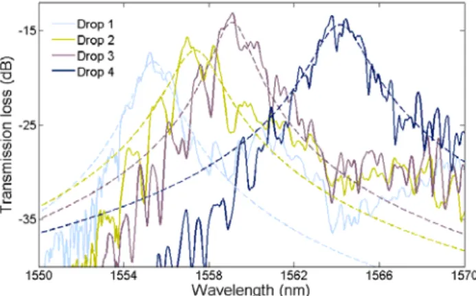
Fig. 2 shows the transmission spectra for each drop port along with their corresponding Lorentzian fits. Results are reported in Tab. 1. Worth noting is the presence of residual oscillations in the transmission spectra. These fringes originate from imperfections, more precisely errors in positioning during the writing of the waveguides by e-beam lithography (stitching), introduced during the fabrication process. The asymmetry of the spectra, on the contrary, results from the dispersion of the photonic crystal waveguides which introduces a wavelength dependent coupling and leads to discrepancies between the fit and the measurement in particular in the blue side of the spectra.
Channel wavelengths are defined at each transmission peak namely 1 = 1554.9 nm, 2 = 1556.7 nm, 3 = 1558.8 nm and
4 = 1563.5 nm leading to channel spacings () ranging between 225 GHz and 580 GHz. Estimated 3 dB spectral
Adjacent channels isolation (ACI) is determined by injecting four signals at the four channel wavelengths and by measuring the relative attenuation of the channel under test compared with its adjacent channels. The ACI spans from 8.5 dB to 20 dB depending on the port, with lowest values of isolation (8.5 dB) measured at the output of port 2, as shown by the spectrum reported in Fig. 3. The demultiplexer was
designed to operate from 1552 nm to 1565 nm with a
bandwidth of 1.9 nm and a channel spacing of about 500 GHz (channel spacing chosen for demultiplexing feasibility study). The agreement with respect to the original design is quite good (less than 0.35 nm error on the bandwidth, less than 3 nm on the central frequency) except for the distribution of the resonances which are not equidistant in wavelength (error of the order of 300 GHz on channel spacing). The total insertion losses at the resonance of each stage range from 11 to 16 dB depending on the considered channel.
The drop efficiency (Deff) is commonly defined as the ratio of the power driven by the cavity from the bus to the drop channel with respect to the power on the bus (evaluated immediately before and after the cavity) [7]. As these sections are not directly accessible for the measurement, Deff has been estimated through the power levels at the external ports (drop and input) and considering coupling, bend and waveguide propagation losses. In our device, the coupling loss per face and waveguide loss for the TE mode are estimated to be 3 dB and 1 dB/mm respectively [9]. The estimated drop efficiency
thus varies from 13.5 % to 42.6 %, depending on the
considered channel. The drop efficiency of the best channel is very close to the theoretical value of 50 % that can be reached for a 3-port filter designed with a H0 cavity [13].
Fig. 2. Transmission through the drop channels of the PhC filter with corresponding Lorentzian fits at 0 dBm input power.
580 260 225 (GHz) 33.9 42.6 16.9 13.5 Deff(%) 20 13 8.5 10 ACI (dB) 2.20 1.60 2.15 1.65 Width (nm) 12 11 15 16 Loss (dB) 1563.5 1558.8 1556.7 1554.9 (nm) 4 3 2 1 Channel 580 260 225 (GHz) 33.9 42.6 16.9 13.5 Deff(%) 20 13 8.5 10 ACI (dB) 2.20 1.60 2.15 1.65 Width (nm) 12 11 15 16 Loss (dB) 1563.5 1558.8 1556.7 1554.9 (nm) 4 3 2 1 Channel
Table 1. Characterization of drop channels.
Port 2 8.5 dB -80 -60 -40 -20 Po w e r ( d B m ) 1554 1558 1562 Wavelength (nm) 8.5 dB Port 2 8.5 dB -80 -60 -40 -20 Po w e r ( d B m ) 1554 1558 1562 Wavelength (nm) 8.5 dB
III. SYSTEM EXPERIMENT
As these first experimental results demonstrate the possibility to efficiently separate the four channels of the WDM frame, we then proceed with the characterization by investigating the performance of the filter as a demultiplexer for a WDM system.
The experimental setup is shown in Fig. 4. As it can be observed, the four channels coming from the different laser sources are combined in pairs through two 3 dB couplers. Channel wavelengths are those specified in Tab. 1 (see inset in Fig. 4). The NRZ signals are then generated by two
Mach-Zehnder modulators MZ1 and MZ2 with 231-1 Pseudo
Random Bit Sequences (PRBS) at 25 Gbit/s. MZ1 modulated channels 1 and 3 whereas MZ2 modulated the interleaved 2 and 4 channels. These signals are eventually combined by another 3 dB coupler before passing through an erbium doped fiber amplifier (EDFA1). The 12 nm filter which follows the amplifier is used in order to limit optical noise. After that, the signals are adjusted to the TE polarization mode by the PC and then coupled into the DUT via a micro-lensed fiber. The power of each channel at the input of the DUT is -7 dBm. Signals at the output of the DUT are then amplified again (EDFA2) and sent to the receiver. The power at the receiver is adjusted by a variable attenuator (VA). The 1 nm filter placed before the power-meter is used in order to select the channel under study.
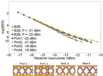
This setup has been used to analyze the bit error rate (BER) evolution as a function of the input power at the receiver for all output ports of the device. Results are reported in Fig. 5. To evaluate the performance of the filter we measured the power penalty, i.e. the power increase needed at the receiver to guarantee a BER of 10-9 with respect to the power required for the same BER in the back-to-back (B2B) experiment. In the B2B configuration, the DUT has been replaced by a flat-top filter: this configuration is therefore considered as the reference for performance evaluation. The corresponding results are illustrated by the dashed line with empty circles in Fig. 5.
To demonstrate that the cross talk is negligible in the measurement setup, and possibly introduced by the DUT, the B2B experiment has been performed in a first time with only one active channel in the system and then with all channels turned on, obtaining perfectly superimposed curves (not reported here because indistinguishable from B2B).
Now when the device is introduced, no power penalty has been measured on channels 3 and 4 (squares and crosses on Fig. 5), thus demonstrating a negligible crosstalk on these channels. On the contrary, on channels 1 and 2 we have observed a power penalty of 0.8 dB (full circles, continuous line) and 1.1 dB (triangles, continuous line) respectively at a BER of 10-9. To explain the measured penalty on these two channels, we have performed B2B experiments with input powers at EDFA2 equal to the powers at the filter output of the port 1 (-22 dBm) and 2 (-21 dBm) (full circle and triangles dotted lines respectively). As one can observe, for channel 1 the curve through the filter is superimposed to the B2B curve at -22 dBm. Degradation of Optical Signal to Noise Ratio (OSNR) for this channel, determined by the reduced Deff of channel 1, is thus the cause of the measured penalty of 1 dB. However, this is not the case for channel 2. In fact, for this channel the B2B curve at -21 dBm performs better than the curve obtained for port 2. The additional penalty is unveiled by looking at the eye diagrams at the output of each port (inset of Fig. 5). As it can be observed, a “double line” determined by the interference of the adjacent channels appears in the eye diagram of the second port, where channel 2 is received. This is therefore a crosstalk effect which is probably related to the perturbated transmission owing to fabrication imperfections [14, 15], which is also at the origin of the low ACI value (8.5 dB, see Fig. 2).
Additional measurements were performed on channel 2 in order to evaluate the inter-channel crosstalk effects. The setup is similar to Fig. 4 except that, during the test, the central wavelength on port 2 has been locked at 2 = 1556.7 nm while the wavelengths of adjacent channels (i.e. channel 1 and channel 3) have been modified. In the first experiment, 1 is fixed at 1554.9 nm whilst 3 has been varied; in the second one, 3 was tuned at 1559.1 nm whereas 1 has been detuned with respect to 2. In both experiments, for each value of the channel spacing the BER has been recorded as a function of the receiver input power, thus allowing for extrapolating the
PC DUT VA Ch.#2 25 Gbit/s PRBS 231-1 sequence Ch.#4 Ch.#1 25 Gbit/s PRBS 231-1 sequence Ch.#3 MZ1 MZ2 3dB coupler 3dB coupler 3dB coupler EDFA1 Receiver Power -meter EDFA2 12nm 1nm 1554 1556 1558 1560 1562 1564 -50 -40 -30 -20 -10 0 Wavelength (nm) Po w e r ( d B m ) 1 2 4 1 2 4 PC DUT VA Ch.#2 25 Gbit/s PRBS 231-1 sequence Ch.#4 Ch.#1 25 Gbit/s PRBS 231-1 sequence Ch.#3 MZ1 MZ2 3dB coupler 3dB coupler 3dB coupler EDFA1 Receiver Power -meter EDFA2 12nm 12nm 1nm 1554 1556 1558 1560 1562 1564 -50 -40 -30 -20 -10 0 Wavelength (nm) Po w e r ( d B m ) 1554 1556 1558 1560 1562 1564 -50 -40 -30 -20 -10 0 Wavelength (nm) Po w e r ( d B m ) 1554 1556 1558 1560 1562 1564 -50 -40 -30 -20 -10 0 Wavelength (nm) Po w e r ( d B m ) 1 2 4 1 2 4
Fig. 4. Experimental setup of 4-channel demultiplexing.
Port 1 Port 2 Port 3 Port 4
Port 1 Port 2 Port 3 Port 4
Port 1 Port 2 Port 3 Port 4
Fig. 5. BER versus receiver input power in WDM experiment. Inset: eye diagrams at the output of each port with time window of 200 ps.
degradation, BER measurements have been performed with the same input power on EDFA2 (triangles dotted line relative to B2B -21 dBm in Fig. 5).
Power penalty as a function of channel spacing measured in both experiments is presented in Fig 6. It is worth noting that when the channel spacing is above 300 GHz the power penalty induced by the presence of adjacent channels is negligible (0.3 dB). However, it increases rapidly when 3 approaches 2, due to the high transmission of port 2 at 212 GHz away from its central wavelength (Fig. 6. inset). The lobe of the transmission curve in the opposite side at 162 GHz away from 2 also causes 2.5 dB of power penalty when 1 reaches that point.
From the results shown in Fig 6 we conclude that, in order to keep the penalty lower than 1 dB, the channel spacing must be higher than 250 GHz (between 3 and 2) and 210 GHz (between 1 and 2). These constraints on channel spacing could be relaxed by a better control of the fabrication process, which is expected to be achieved in the next device generation.
IV. CONCLUSION
In summary, we have demonstrated the first 100 Gbit/s 4-channel WDM (425 Gbit/s) demultiplexing in a system experiment using optical filters based on III-V semiconductor photonic crystals technology. Error-free channel demultiplexing was performed using a four stage filter with low cross-talk power penalty (<1 dB). These results show the strong potential of such a technology for ultra compact all-optical signal processing.
the performance of two dimensional photonic crystal based bandpass filter”, Optical and Quant. Electron., vol. 43, n°6-10, pp. 69-82, 2012. [2] F. Van Laere, T. Stomeo, C. Cambournac, M. Ayre, R. Brenot,
H. Benisty, G. Roelkens, T. F. Krauss, D.V. Thourhout and R. Baets, “Nanophotonic Polarization Diversity Demultiplexer Chip”, J. Lightwave Tech., vol. 27, n°4, pp. 417-425, 2009.
[3] T. Niemi, L. H. Frandsen, K.K. Hede, A. Harpoth, P. I. Borel and M. Kristensen, “Wavelength-division demultiplexing using phtonic crystal waveguides”, Phot. Tech. Letters, vol. 18, n°.1, pp. 226-228, 2006.
[4] H. Takano, B. S. Song, T. Asano and S. Noda, “Highly efficient multi-channel drop filter in a two-dimensional hetero photonic crystal”, Opt. Express, vol. 14, n°8, pp.3491–3496, 2006.
[5] J. J. Vegas Olmos, M. Tokushima and K. Kitayama, “Photonic Add– Drop Filter Based on Integrated Photonic Crystal Structures”, J. Selec. Top. in Quant. Elect., vol. 16, n°1, pp. 332-337, 2010.
[6] S. Combrié, G. Lehoucq, S. Xavier, A. De Rossi, K. Lenglé, L. Bramerie, M. Gay, J.C. Simon, G. Bellanca, S. Malaguti and S. Trillo., “40 Gb/s Wavelength Division Demultiplexing with a PhC Filter”, Proc. MOC, Sendai, Japan, 2011.
[7] H. Ren, C. Jiang, W. Hu, M. Gao and J. Wang, “Photonic crystal channel drop filter with a wavelength-selective reflection micro-cavity”, Optics Express, vol. 14, n°6, pp. 2446-2458, 2006.
[8] S. Combrié, E. Weidner, A. DeRossi, S. Bansropun, and S. Cassette “Detailed analysis by Fabry-Perot method of slab photonic crystal line-defect waveguides and cavities in aluminium-free material system”, Opt. Express, vol. 14, n°16, pp.7353–7361, 2006.
[9] Q.V. Tran, S. Combrié, P. Colman and A. De Rossi., “Photonic crystal membrane waveguides with low insertion losses”, Appl. Phys. Letters, vol. 95, pp. 061105, 2009.
[10] L. Frandsen, A. Harpøth, P. Borel, M. Kristensen, J. Jensen and O. Sigmund, “Broadband photonic crystal waveguide 60° bend obtained utilizing topology optimization”, Opt. Express, vol 12, n°24, pp. 5916-5921, 2004.
[11] M. Thual P. Rochard, P. Chanclou and L. Quetel, “Contribution to research on Micro-Lensed Fibers for Modes Coupling”, Fiber and Integrated Optics, vol. 27, n°6, pp. 532-541, 2008.
[12] Z. Zhang and M. Qiu, “Small-volume waveguide-section high Q microcavities in 2D photonic crystal slabs”, Opt. Express , vol. 12, n°17, pp. 3988-3995, 2004.
[13] H. Ren, C. Jiang, W. Hu, M. Gao, Y. Qu and J. Wang, “Channel drop filter in two-dimensional triangular lattice photonic crystals”, J. Opt. Soc. Am A, vol. 24, A7-A11, 2007.
[14] E. Kuramochi M. Notomi, S. Hughes, A. Shinya, T. Watanabe, and L. Ramunno, “Disorder-induced scattering loss of line-defect waveguides in photonic crystal slabs”, Phys. Rev. B, vol. 72, n°16, pp.161318, 2005.
[15] M. Patterson, S. Hughes, S. Combrié, N.-V.-Quynh Tran, A. De Rossi, R. Gabet, and Y. Jaouën, “Disorder-Induced Coherent Scattering in Slow-Light Photonic Crystal Waveguides”, Phys. Rev. Lett., vol. 102, n°25, pp. 253903, 2009. (b) (a) (c) Relative frequency (GHz) (b) (a) (c) Relative frequency (GHz)
Fig. 6. (a) Power penalty at a BER = 10-9 on port 2 vs. ch. spacing with 1
(triangles) or 3 (circles) varying. (b) Normalized transmission of port 2.