Journal of Fundamental and Applied Sciences is licensed under aCreative Commons Attribution-NonCommercial 4.0 International License.Libraries Resource Directory. We are listed underResearch Associationscategory.
NUMERICAL SIMULATION OF SOLAR CELLS BESED CZTS BUFFER LAYER
(ZnO1-XSX) USING SCAPS-1D SOFTWARE
S. Fadili*1, B. Hartiti1,2, Z. El khalidi1, A. Kotbi1,3, A. Ridah3and P. Thevenin4
1
FST Mohammedia, Hassan ll University Casablanca, Morocco 2
ICTP-UNESCO-IAEA, Trieste, Italy 3
FS Ben M’sik, Hassan ll University Casablanca, Morocco
4
LMOPS Laboratory, Univesity Lorraine, France
Received: 26 November 2016 / Accepted: 24 April 2017 / Published online: 01 May 2017
ABSTRACT
Cds buffer layer has many advantages such as large bandgap, and the carrier density. Otherwise, the presence of cadmium is an inconvenient. Research work, are shifted on the possibility of replacing CdS by a buffer layer devoid of cadmium. This manuscript presents the numerical study, using SCAPS-1D program, the effects of sulfur content in the buffer layer Zn (O,S) on the electrical parameters of the solar cell ZnO: Al / i-ZnO / Zn (O, S) / CZTS /. Changes in the band gap and electron affinity of Zn (O, S) were calculated from the law of Vegard. The numerical results of the thickness of the absorbent layer CZTS equal to 2.5µm, show that from the sulfur content equals to 45% we can find the same results with CdS, an efficiency varies slightly, about 19%.
Keywords: CZTS; ZnO1-xSx; CdS; SCAPS; Solar cells.
Author Correspondence, e-mail:[email protected]
doi:http://dx.doi.org/10.4314/jfas.v9i2.25 ISSN 1112-9867
1. INTRODUCTION
The interest of the quaternary kësterite Cu2ZnSnS4 (CZTS) for solar cells based on four main factors. First, the band gap of the semiconductor, which is between 1.4 eV and 1.5 eV, allows using a larger part of the solar spectrum. Secondly, its absorption coefficient is high with a value of 104 cm-1. Thirdly, it is formed from abundant elements and cheaper than indium or gallium. Finally, its toxicity is less than that of some other materials containing cadmium and selenium. The standard photovoltaic devices based CZTS consist of a thin-film multilayer Mo / CZTS / (CdS, Zn (O, S),...) / i-ZnO / ZnO: Al. A back metal electrode Molybdenum (Mo), an absorbent layer, a fundamental element of the device, CZTS, a buffer layer, respectively ensuring the junction and the absence of circuits (CdS, Zn (O,S),...), a layer of intrinsic ZnO, therefore non-conductive, prevents leakage of current between the absorbent layer and the upper contact, and finally a ZnO optical window doped with aluminum (ZnO: Al) to combine two essential properties, namely electrical conductivity and optical transparency. Work on numerical simulations in the laboratory of CdS buffer layer cells reached an efficiency of around 20% Mostefaoui1 M. et al. [1]. However, their manufacture is the target of much criticism because of the use of cadmium, a toxic material. To remedy this problem, the work was carried out to replace the CdS buffer layer. The authors M. A Olopade. [2], Mr. I. Hossain et al. [3] Peijie Lin et al. [4] and Atul Kumar [5], respectively studied solar cells based on CZTS substituting CdS layer by ZnSe, ZnS, In2S3 and SnS2. An efficiency of approximately 20% is reached by [4]. In this study, we present the results of numerical simulation of the solar cell ZnO: Al / i-ZnO / Zn (O, S) / CZTS /, obtained using the SCAPS-1D software. The CdS buffer layer is replaced by the Zn layer (O, S) of which the band gap and electron affinity are dependent on the sulfur content x = S / Zn. These results concern the effect of this latter and the thickness of the absorbent layer on the electrical characteristics of the solar cell. The originalty and the novelty of this work lies essecialy on the calculation of the the gap energy Eg (CZTS) and the electron affinity in function of the sulfur. We confirm that, through these results that our work is original compared to the litterature. Although, in the field of photovoltaic systems, the materials chosen are abundant, have an important characteristics, and the study made is relevant when we investigate the effect of sulfur on the layers studied. This
work is also preceded by an experimental synthesis of the thin films such as: ZnO, CIGS [6-8] made in our laboratory, although this study is established to predict the behavior of the solar cell based on the material elaborated in term of simulation.
2. RESULTS AND DISCUSSION
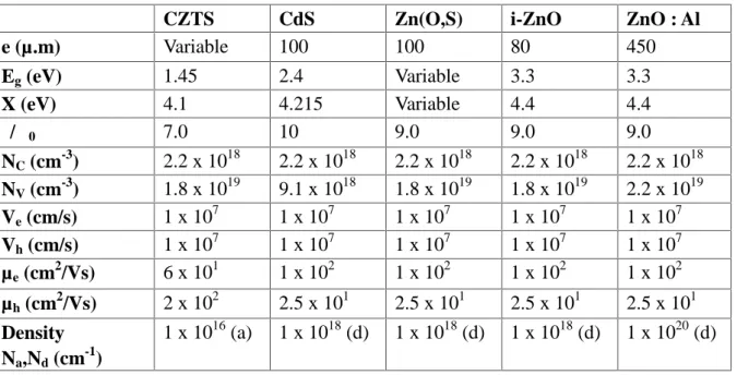
The solar cell that we studied is shown in Figure-1. It consists of four layers of ZnO: Al / i-ZnO / Zn (O, S) / CZTS /. For the numerical simulation, we used the SCAPS-1D software developed at the Electronics Department and Information Systems at the University of Ghent, Belgium [9]. The material parameter values used in the simulation are considered constant and taken from the manuscript of Mr. Djinkwi Wanda et al. [10] Table 1. The change of the band gap is calculated from equation [11] and the electron affinity of the ZnO1-xSxbuffer layer according to the Vegard law [12]. Depending on the sulfur rate x = S / Zn, Eg (ZnO1-xSx) and (ZnO1-xSx) are written:
Eg(ZnO1-xSx) = x.Eg(ZnS) + (1-x).Eg(ZnO) – b..x(1-x)
(ZnO1-xSx) = x.(ZnS) + (1-x).(ZnO) where:
Eg(ZnS) = 3.6 eV, Eg(ZnO) = 3.3 eV, (ZnS) = 3.88 eV, (ZnO) = 4.45 eV and b = 3.1 eV is the curvature parameter.
ZnO: Al i-ZnO Zn(O,S)
CZTS
Table 1. Physical paameters used in the simulation
2.1. Solar cell CdS buffer layer
Initially we studied the cell's response CZTS / CdS / i-ZnO / ZnO: Al. The thickness of the absorbing layer is equal to 2.5. The curve of Figure 2 represents the variation of current J depending on the potential difference V. The values of Jsc, Voc, FF, and ETA are 23.86 mA, 0.9573 V, 84.62% and 19.33% respectively. As a continuation of this work we will investigate the sulfur content in Zn (O, S) and the thickness of the absorbent layer CZTS that allow to approach the value of 19.33% in the case of the cell CZTS / Zn (O, S) / i-ZnO / ZnO: Al.
CZTS CdS Zn(O,S) i-ZnO ZnO : Al
e (µ.m) Variable 100 100 80 450 Eg(eV) 1.45 2.4 Variable 3.3 3.3 X (eV) 4.1 4.215 Variable 4.4 4.4 ɛ/ ɛ0 7.0 10 9.0 9.0 9.0 NC(cm-3) 2.2 x 10¹⁸ 2.2 x 10¹⁸ 2.2 x 10¹⁸ 2.2 x 10¹⁸ 2.2 x 10¹⁸ NV(cm-3) 1.8 x 10¹⁹ 9.1 x 10¹⁸ 1.8 x 10¹⁹ 1.8 x 10¹⁹ 2.2 x 10¹⁹ Ve(cm/s) 1 x 10⁷ 1 x 10⁷ 1 x 10⁷ 1 x 10⁷ 1 x 10⁷ Vh(cm/s) 1 x 10⁷ 1 x 10⁷ 1 x 10⁷ 1 x 10⁷ 1 x 10⁷ µe(cm2/Vs) 6 x 101 1 x 10² 1 x 10² 1 x 10² 1 x 10² µh(cm2/Vs) 2 x 10² 2.5 x 101 2.5 x 101 2.5 x 101 2.5 x 101 Density Na,Nd(cm-1) 1 x 10¹⁶(a) 1 x 10¹⁸(d) 1 x 10¹⁸(d) 1 x 10¹⁸(d) 1 x 10²⁰(d)
Fig.2. J(V) curve of the cell with CdS buffer layer
2.2. Solar cell with ZnO1-xSxbuffer layer
2.2.1 Efficiency curves and relative error
To replace the CdS buffer layer by ZnO1-xSx buffer layer where x is the sulfur content in the layer, we traced the curve of ETA electronic efficiency in function of x with a thickness of CZTS equal to 2.5 (Figure 3). For a value of x = 0.45 ETA exceeds the value 19%.
We define the efficiency relative error
Cds x Cds r R R R
E function of x represented in the
curve of Figure 4. RCdS is the efficiency of the solar cell, the cell CZTS / CdS / i-ZnO / ZnO:Al. It is noted that, for a sulfur content x = 0.45, Er is not exceeding 1.5%. This value could be reduced by increasing the thickness of the absorbent layer CZTS.
Fig.3. Efficiency urve ETA based on sulfur rate x layer CZTS / Zn (O, S) / i-ZnO / ZnO: Al.
2.2.2 Curves of the electrical characteristics for x=0.45
To reduce the value of the relative error Erbetween the efficiency of the cell CdS buffer layer and that of the buffer layer Zn (O, S), we studied the variations in the electrical characteristics of the cell depending on the thickness of the absorbent layer CZTS. All photovoltaic cell parameters increase with thickness, the open circuit voltage Voc (Figure 5), the circuit currant Isc (Figure 6), the fill factor FF (Figure 7) and in particular the efficiency conversion (Figure 8) which passes from 9.1% for a thickness of 0.5 µm up to 21.19% for a thickness of 4 µm. This could be explained by the fact, that with the increase of the thickness of the CZTS layer, the absorption of photons of short wavelength increases, which promotes photo-generation of additional free carriers.
From the curve of (Figure 8), we can deduce the thickness of the layer CZTS corresponding to an efficiency close to the value 19.33%. This thickness is of the order of 2.63 µm.
Fig.6. Curve of circuit current Icc according to the thickness of CZTS.
Fig.8. Efficiency curve current ETA corresponding to the thickness of CZTS.
4. CONCLUSION
In this manuscript, we studied the electrical properties of the solar cell ZnO: Al / i-ZnO / ZnO1-xOx / CZTS / depending on the sulfur rate x and the thickness of the absorbent layer. The goal was to replace the CdS buffer layer by ZnO1-xOx, a free layer of cadmium, toxic materials. For this, we used the SCAPS-1D software. We treated the example of the cell-based CZTS whose physical and geometrical parameters of the thin films, and were taken from literature. The band gap and electron affinity of ZnO1-xOx are calculated based on the sulfur rate x. The results showed that it was possible for a fixed amount of sulfur in the ZnO1-xSx buffer layer; we can deduce the thickness of the absorbent layer, which allows finding the efficiency of the solar cell CdS buffer layer.
6. REFERENCES
[1] M. Mostefaoui, H. Mazari, S.Khelifi1, R.Dabou, ‘’Effect of a buffer layer on the Performance of Thin-film Cu(In,Ga)Se2 Solar Cells’’. Journal of New Technology and
[2] M. A. Olopade, O. Oyebola and B. S. Adeleke, “Investigation of some materials as buffer layer in copper zinc tin sulphide (Cu2ZnSnS4) solar cells by SCAPS-1D,” Advances in Applied Science Research, 3 (6), pp.3396-3400, 2012.
[3] M. I. Hossain.P. Chelvanathan, M. M. Alam, M. Akhtaruzzaman, K. Sopian and N. Amin,
“Potential Buffer Layers For Cu2ZnSnS4 (CZTS) Solar Cells from Numerical Analysis,”
presented at the IEEE Conference on Clean Energy and Technology, Langkawvi, Malaysia, 18 Nov – 20 Nov 2013, pp. 450-454.
[4] Peijie Lin, Lingyan Lin , Jinling Yu, Shuying Cheng, Peimin Lu and Qiao Zheng,
“Numerical Simulation of Cu2ZnSnS4 Based Solar Cells with In2S3 Buffer Layers by
SCAPS-1D,” Journal of Applied Science and Engineering, Vol. 17, No. 4, pp. 383-390, 2014. [5] Atul Kumar and Ajay D Thakur, “Analysis Of SnS2 Buffer Layer And SnS Back Surface
Layer Based CZTS Solar Cells Using SCAPS,” arXiv: 1510, 2015.
[6] H. Tghonia et al, Solution-based deposition of wurtzite copper zinc tin sulfide nanocrystals as a novel absorber in thin film solar cells. Optiacal quantum electronics, DOI: 10.1007/s11082-016-0535-9, 2016
[7] A. Kotbi et al, Characteristics of CuInS2 thin films synthesizes by chemical spray pyrolysis, DOI: 10.1007/s11082-015-0344-6, 2016.
[8] Z. El khalidi, Elaboration of ZnO: Ga thin films by spray pyrolysis for photovoltaic applications. P: 1161 – 1165, 3-936338-41-8. Proceeding European PV Solar Energy Conference and Exhibition Germany, 2016.
[9] http://scaps.elis.ugent.be/
[10] M. Djinkwi Wanda, S. Ouédraogo, F. Tchoffo, F. Zougmoré, and J. M. B. Ndjaka ‘’Numerical Investigations and Analysis of Cu2ZnSnS4 Based Solar Cell by SCAPS-1D’’. Volume 2016 (2016), Article ID 2152018, 9 pages
[11] M. Buffière, S. Harel1 , C. Guillot-Deudon1 , L. Arzel1 , N. Barreau1 , and J. Kessler1,2
“ Effect of the chemical composition of co-sputtered Zn(O,S) buffer layers on Cu(In,Ga)Se2 solar cell performance” Phys. Status Solidi A 212, No. 2, 282–290 (2015) / DOI
10.1002/pssa.201431388
Philip Thevenin ‘’ Performances des cellules à base de Cu2ZnSnS4 (CZTS) : Une analyse par simulations numériques via le simulateur SCAPS. Afrique SCIENCE 11(4) (2015) 16 – 23
How to cite this article:
Fadili S, Hartiti B, El khalidi Z, Kotbi A, Ridah A and Thevenin P. Numerical simulation of solar cells besed czts buffer layer (ZnO1-XSX) using scaps-1d software. J. Fundam. Appl. Sci., 2017, 9(2), 1001-1011.