Pépite | Techniques de traitement numérique en temps continu appliquées à l'égalisation de canal pour communications millimétriques à faible consommation
114
0
0
Texte intégral
(2) Thèse de Ilias Sourikopoulos, Lille 1, 2015. 2 © 2015 Tous droits réservés.. doc.univ-lille1.fr.
(3) Thèse de Ilias Sourikopoulos, Lille 1, 2015. ABSTRACT Receivers for 60GHz wireless communications have been profiting from innovation in wired links in order to meet a power budget that will enable integration in next‐generation high-speed portable wireless terminals. Mixed‐signal implementations of the Decision Feedback Equalizer (DFE) have been proposed to alleviate overall system consumption. In this thesis, power minimization is pursued by removing the clock from the feedback path of the DFE. Inspired by recent developments in Continuous‐Time Digital Signal Processing, a continuous‐time digital delay line is used. The design aims at mitigating wireless channel impairments caused by signal reflections in typical Line‐of‐Sight, indoors deployment conditions. The system is shown theoretically to achieve channel‐dependent power consumption within acceptable Bit Error Rate performance for decoding. Moreover, a programmable digital delay element is proposed as the granular element of the delay line that exploits body biasing to achieve a coarse/fine functionality. Prototype DFE and delay lines have been fabricated and characterized in 28nm Fully Depleted Silicon Over Insulator technology (FDSOI).. RÉSUMÉ Les récepteurs pour les communications sans fil très haut débit à 60 GHz tirent profit des innovations des liens filaires afin de réduire le budget de puissance, ce qui permettra l’'intégration de la prochaine génération des terminaux portables sans fil. L’implémentation d’un égaliseur de canal à décision rétroactive, utilisant des signaux mixtes, est proposé pour diminuer la consommation globale du système. Dans ce mémoire, la réduction de consommation est atteinte par l'élimination de l'horloge du chemin de rétroaction de l’égaliseur. Inspiré par des récents développements en traitement des signaux numériques en temps continu, une ligne à retard numérique est aussi introduite. Le système conçu vise à atténuer les effets causés par les réflexions du signal dans des contextes de transmission en contact visuel entre le transmetteur et le récepteur. Les résultats théoriques montrent ainsi une consommation dépendante de la réalisation du canal. En outre, un élément de délai numérique programmable est proposé en tant qu’élément granulaire de la ligne à retard, en exploitant la polarisation de substrat des transistors, afin d’atteindre un réglage des délais extrêmement fin. Des démonstrateurs sur Silicium ont été fabriqués et caractérisés en technologie 28 nm FDSOI (Fully Depleted Silicon Over Insulator) pour démontrer les concepts proposés dans cette thèse.. 3 © 2015 Tous droits réservés.. doc.univ-lille1.fr.
(4) Thèse de Ilias Sourikopoulos, Lille 1, 2015. Ilias Sourikopoulos IEMN/ISEN Dpt. SMART/CCI 41, Bd. Vauban 59046 Lille CEDEX ilias.sourikopoulos@isen.fr ilias.sourikopoulos@ed.univ-lille1.fr. Notice for manuscript – library archival version, Μay 2016: This manuscript version contains previously unpublished circuits and measurement results. It is released exclusively for library archiving and internal registering.. 4 © 2015 Tous droits réservés.. doc.univ-lille1.fr.
(5) Thèse de Ilias Sourikopoulos, Lille 1, 2015. “Choose to be happy” - Iliana. 5 © 2015 Tous droits réservés.. doc.univ-lille1.fr.
(6) Thèse de Ilias Sourikopoulos, Lille 1, 2015. 6 © 2015 Tous droits réservés.. doc.univ-lille1.fr.
(7) Thèse de Ilias Sourikopoulos, Lille 1, 2015. ACKNOWLEDGEMENTS. This thesis was carried out working around exquisite people. If only I could enumerate how each one of them helped me along this four year path, I would need a tome. I feel genuinely lucky I had the opportunity to work around them. I wish to extend my gratitude to my thesis directors Andreas Kaiser and Laurent Clavier for their leadership and insight that brought this thesis to fruition. Same goes to my ISEN advisor Antoine Frappé, whose guidance and commitment to this project was inexhaustible. He worked hard to keep me firmly oriented towards the goal and took a fair part in the mental rollercoaster involved, especially during the peak workloads of taping-out and measuring. I would also like to thank the reporters and members of my jury for accepting my director’s invitation to review my work. Their remarks, comments and corrections are an exceptional opportunity for me to improve this work. Special thanks go to my industrial partner STMicroelectronics and personally Andreia Cathelin who not only managed access to high-end fabrication technology but was always there to receive the pitch and calibrate the ideas. Bruno Stefanelli’s contribution for this work was also crucial. He helped in so many different ways in design, assembly and test. He was an unequivocal voice of reference. Axel Flament and Jean-Marc Capron provided various comments and advice in the process. I used Axel’s DAC design on my chip and Jean-Marc’s next door design solidarity. Emmanuel Dubois and David Delcroix have been my assembly wizards. Die laser cutting on a droplet of water(!) and pad-side-wedge-land-side-ball bonding(!) actually permitted to have the measured silicon results presented in this thesis. (For a moment process engineering seemed like a decent dayjob.) I would like to thank Valerie Vandenhende for her warmth and attention especially through my early days in France and her friendship throughout the years. Florence Alberti has acted in times as my psychotherapist as well as administration companion across the hall. I’m thankful she has been usually the first person to say hello to. I would like also to thank Olivier Irrmann for after-hours humor and for opening a door to the dark side and Marta for a great message of encouragement. 7 © 2015 Tous droits réservés.. doc.univ-lille1.fr.
(8) Thèse de Ilias Sourikopoulos, Lille 1, 2015. Jean-Charles Caillez for arranging funding to attend an unforgettable MOSAIC workshop in Lille. Thanks to the colleagues and organizing committee in #Doctoriales2014. I had a burnout week to build an award winning Toy Company and in maThèse180 for glorious fun and stardom exposure. Special thanks to the scientific director of College Doctoral Laurence Duchien and my “Prise de parole en Public”coach Geraldine BESSON. Thanks to the Centre National de la Rcherche Scientific (CNRS) for funding this work as well as an encouraging cuisine. I would like to thank my friends, the skin of the earth yesterday, leaders of industry and academia tomorrow (or whatever they choose to be, for that matter), my fellow PhD students past and present. Hani was my anchor point the first months. I miss working with him around global politics and current affairs. I shared a lot of interesting discussions with Fawzi, I regard him a brilliant man and I was sad to see him leave. I appreciated the humor of Arnaud and the always cheerful demeanor of Baptiste. Pietro assigned me my first tape-out deal, it was evident this guy wouldn’t escape from academia. With Stéphane, we had high spirited debates over channel equalization and estimation for a year, I thank him for making me part of his work. Camillo saved the day in the end of his tour of duty in ISEN I wish him well overlooking the lake and Matteo is always a pleasure to have around, I might follow in his footsteps soon. My greetings to our newly welcome member in the lab, Dipal and all my support and “Bon Courage” to Fikre and Cristian on their way to the top of their efforts. Thank you for keeping me sane. I cannot thank you enough, Iliana, for your patience and your support through this. This goes out to you, my family and the friends I miss.. 8 © 2015 Tous droits réservés.. doc.univ-lille1.fr.
(9) Thèse de Ilias Sourikopoulos, Lille 1, 2015. CONTENTS CHAPTER 1. INTRODUCTION. 18. 1.1. A gun that fired 100 years later. 20. 1.2. The never ending revolution. 21. 1.3. All is digital, but what about timing?. 23. 1.4. Thesis contribution. 24. 1.5. Thesis organization. 24. 1.6. Chapter Bibliography. 25. CHAPTER 2 2.1. CONNECTED WITHIN CLOSED DOORS. Communicating through the 60GHz channel. 28 29. 2.1.1. Free space loss and beamforming. 29. 2.1.2. Penetration and reflectivity. 31. 2.1.3. Multipath propagation and Inter-Symbol Interference. 32. 2.1.4. Features of channel modeling. 35. 2.1.5. Simulating 60GHz channels. 36. 2.2. Equalization for 60GHz channel receivers. 38. 2.2.1. OFDM and Frequency domain equalization. 39. 2.2.2. Time domain equalization. 42. Decision feedback equalization. 43. 2.3 2.3.1. Employing the DFE: from Gigabit wired to Gigabit wireless. 45. 2.4. State of the art mixed-signal DFEs in 60GHz receiver basebands. 47. 2.5. Chapter Bibliography. 50. CHAPTER 3. A 60GHZ BASEBAND DFE WITH CHANNEL DEPENDENT POWER. CONSUMPTION 3.1. Critical tap cancellation. 56 57. 9 © 2015 Tous droits réservés.. doc.univ-lille1.fr.
(10) Thèse de Ilias Sourikopoulos, Lille 1, 2015. 3.2. A DFE with channel dependent power consumption. 61. 3.2.1. Continuous-time digital feedback filtering for the DFE. 61. 3.2.2. Continuous-time digital delay element with two-stage control. 63. 3.2.3. Power consumption comparison against the clocked approach. 64. 3.2.4. A DFE consumption profile linked to the channel realization. 65. 3.3. Chapter Bibliography. CHAPTER 4. CONTINUOUS-TIME DIGITAL DELAY-LINE IN 28NM FDSOI. 66. 68. 4.1. General delay line specification. 69. 4.2. Digital delay elements - state of the art. 69. 4.2.1. Cascaded inverters. 71. 4.2.2. Capacitive Shunting. 71. 4.2.3. Semi-static approach. 72. 4.2.4. Current-starving. 73. 4.2.5. Thyristor-based delay element. 75. 4.2.6. Discussion. 78. 4.3. Prototype back-gate driven thyristor based delay line in 28nm FDSOI. 79. 4.3.1. Proposed Delay element design. 80. 4.3.2. Delay versus control. 82. Delay line prototyping. 85. 4.4 4.4.1. Post-layout simulation results. 87. 4.4.2. Chip design. 88. 4.5. Measurement results. 89. 4.6. Chapter bibliography. 100. CHAPTER 5. A 5-TAP MW/GBPS DFE FOR 60GHZ BASEBANDS. 103. 5.1. Specification of the proposed DFE. 104. 5.2. Prototype DFE circuit design. 105. 5.2.1. Principle of operation. 105. 5.2.2. Transistor level design. 106. 5.2.2.1. Analog summer. 106. 10 © 2015 Tous droits réservés.. doc.univ-lille1.fr.
(11) Thèse de Ilias Sourikopoulos, Lille 1, 2015. 5.2.2.2. Comparator. 109. 5.2.2.3. Comment on first-tap implementation. 109. 5.3. Chip design. 110. 5.4. Measurement Results. 111. 5.5. Chapter Bibliography. 111. 11 © 2015 Tous droits réservés.. doc.univ-lille1.fr.
(12) Thèse de Ilias Sourikopoulos, Lille 1, 2015. LIST OF FIGURES Fig. 1-1. The first phonautograph..................................................................................................................................... 18 Fig. 1-2. A 37.000 year old “hello world”........................................................................................................................ 18 Fig. 1-3. “Télégraphe de Chappe” named after the inventor. ................................................................................. 19 Fig. 1-4 FD-SOI transistor cross-section [STMicro]. .................................................................................................. 22 Fig. 1-5 Continuous-time digital signal processor block diagram [Tsividis, 2006]. ..................................... 23 Fig. 2-1 Average atmospheric absorption of millimeter waves [FCC, 1997 and Lai, 2008]. ..................... 30 Fig. 2-2 Beamforming principle of operation [Ruckus, 2013]. .............................................................................. 30 Fig. 2-3 3D model of conference room highlighting reception through 1st and 2nd order reflections from the ceiling and walls [Maltsev10]........................................................................................................................... 31 Fig. 2-4 Multipath propagation and channel impulse response from [Molich, 2011]. Echoes of the signal arrive through different paths spreading the channel impulse response in time. .......................... 33 Fig. 2-5 Demonstrating ISI generated by the superposition of three components at the receiver input [Molisch, 2011]. ........................................................................................................................................................................ 34 Fig. 2-6 60GHz channel impulse response structure from [Maltsev, 2014]. ................................................... 35 Fig. 2-7 Impulse response realizations created by the 802.11ad model for a living room setting with (a1, a2) different Tx-Rx distance and (b1, b2) different Rx HPBW. The total power of all cluster rays is normalized to one. ................................................................................................................................................................... 37 Fig. 2-8 Tapped delay line channel model in [Proakis, 2007]. .............................................................................. 38 Fig. 2-9 By applying an MMSE criterion the error between the transmitted signal and the output of the equalizer is minimized. .................................................................................................................................................. 39 Fig. 2-10 Eye diagram with (i) no multipath distortion (ii) one path arriving within symbol time (iii) one path arriving one symbol time later than the previous case. ........................................................................ 40 Fig. 2-11 Principle of a SC-FDE linear equalizer as seen in [Saito, 2013]. ........................................................ 41 Fig. 2-12 Time-domain linear equalizer diagram from [Boccuzzi, 2008]......................................................... 42 Fig. 2-13 Typical structure of a decision feedback equalizer, presented along with a channel impulse response. The feedback filter (FBF) can correct only post-cursor ISI. .............................................................. 44 Fig. 2-14 Backplane channel frequency and impulse response. At very high data rates such as 25Gbps, post-cursor ISI spans 15 taps [Bulchazzelli, 2013]. For a rate of ~2 Gbps one or two taps would suffice. ........................................................................................................................................................................................... 45 Fig. 2-15 Evolution of DFE summers in wired links. (a) Resistively loaded CML summer. (b) Currentintegrating summer. (c) Sampled current integrating summer. (d) Peaking current-integrating summer from [Bulchazzeli, 2013] .................................................................................................................................... 46 Fig. 2-16 Mixed signal equalization relieves the power consumption of the dominating DSP block. .. 47 Fig. 2-17 Mixed-signal baseband in [Sobel10]. ............................................................................................................ 48. 12 © 2015 Tous droits réservés.. doc.univ-lille1.fr.
(13) Thèse de Ilias Sourikopoulos, Lille 1, 2015. Fig. 2-18 Cascode summation in [Thakkar, 2012]...................................................................................................... 49 Fig. 2-19 Flexible tap allocation in [Sobel, 2009]........................................................................................................ 49 Fig. 3-1 Propagation of two paths within a room and Line-Of-Sight channel impulse response. .......... 57 Fig. 3-2 A typical 60GHz LOS channel impulse response. We remark that ISI is strongly impacted by the indicated, high amplitude components. .................................................................................................................. 58 Fig. 3-3 Worst-case BERs with an increasing number of critical impulse response components cancelled, under Eb/N0=5dB. ............................................................................................................................................. 59 Fig. 3-4 Worst case BER with and without equalization of 5 critical components alongside with the theoretical AWGN channel at 1Gb/s BPSK. ................................................................................................................... 59 Fig. 3-5 BER degrades as coefficient cancellation is performed with less resolution. ................................ 60 Fig. 3-6 The proposed DFE with variable coefficients and delays. ...................................................................... 61 Fig. 3-7 DFE feedback path implementation in [Sobel, 2009] left, and approach in [Park, 2011] right. ......................................................................................................................................................................................................... 62 Fig. 3-8 The DFE delay element and the granular delay circuit used in simulation. .................................... 63 Fig. 3-9 Power efficiency comparison for a delay element. .................................................................................... 64 Fig. 3-10 Consumption comparison between a discrete-time, static delay-line approach and the continuous-time configurable delay architecture. ..................................................................................................... 65 Fig. 4-1 Typical definitions of rise/fall time and rising/falling edge propagation delay. .......................... 70 Fig. 4-2 Programmable delay line in [Li, 2006]. .......................................................................................................... 71 Fig. 4-3 Output slope varies with load capacitance from [Rabaey, 2003]. ....................................................... 72 Fig. 4-4 Capacitive shunting control from [Nejad, 2003]. ....................................................................................... 72 Fig. 4-5 Semi-static approach relieves short-circuit currents in [Jung, 2011] but adds a static consumption overhead. ......................................................................................................................................................... 72 Fig. 4-6 Current starved inverter delay element with analog control from [Nejad, 2003] ....................... 73 Fig. 4-7 Current starved delay element with digital control [Nejad, 2005]. .................................................... 73 Fig. 4-8 Schmitt trigger output stage on current starved delay from [Mahapatra, 2002]. ........................ 74 Fig. 4-9 CMOS thyristor concept in [Kim, 1996].......................................................................................................... 75 Fig. 4-10 Complete thyristor delay element with static triggering in [Kim, 1996]....................................... 76 Fig. 4-11 Enhancing positive feedback with a current source (M9). .................................................................. 77 Fig. 4-12 Delay element in [Kurchuk, 2012]. ................................................................................................................ 77 Fig. 4-13 FDSOI transistor cross-section. ....................................................................................................................... 79 Fig. 4-14 The delay element circuit proposed by this work. .................................................................................. 80 Fig. 4-15 Vc node evolution for a charging(red) or discharging(blue) event. ................................................ 81 Fig. 4-16 Simulation of rising edge delay variation vs. control ............................................................................. 83 Fig. 4-17 Simulation of falling edge delay vs. control................................................................................................ 83. 13 © 2015 Tous droits réservés.. doc.univ-lille1.fr.
(14) Thèse de Ilias Sourikopoulos, Lille 1, 2015. Fig. 4-18 Delay coarse/fine control with gate/body biasing. ................................................................................ 84 Fig. 4-19 Well arrangement for the granular delay cell. .......................................................................................... 85 Fig. 4-20 Delay line block diagram.................................................................................................................................... 86 Fig. 4-21 The ‘lead’ cell between groups enables the output from the previous group and shuts down the rest of the delay line. ....................................................................................................................................................... 86 Fig. 4-22 Simulation of the programmable range for rising edge delay times. .............................................. 88 Fig. 4-23 Delay line prototype built for characterization and die detail with layout inset. The delay line size is 140um x 7um. ...................................................................................................................................................... 89 Fig. 4-24 Rising edge delay vs. gate/body biasing: (i) gate voltage variation: VGn = 0-1V under VBn =0, (ii) body voltage variation: VBn =0-0.8V under VGn =0.3 ........................................................................................... 91 Fig. 4-25 Rising edge delay vs. gate/body biasing: (i)gate voltage variation: VGn =0-1V under VBn =0, (ii) body voltage variation: VBn =0-0.8V under VGn =0.4 ........................................................................................... 91 Fig. 4-26 Rising edge delay vs. gate/body biasing: (i) gate voltage variation: VGn =0-1V under VBn =0, (ii) body voltage variation: VBn =0-0.8V under VGn =0.5 ........................................................................................... 92 Fig. 4-27 Rising edge delay vs. gate/body biasing: (i)gate voltage variation: VGn =0-1V under VBn =0, (ii) body voltage variation: VBn =0-0.8V under VGn =0.6 ........................................................................................... 92 Fig. 4-28 Falling edge delay vs. gate/body biasing: (i) gate voltage variation: VGp =0-1V under VBp =1, (ii) body voltage variation: VBp =1-0.2V under VGp =0.4 ........................................................................................... 93 Fig. 4-29 Falling edge delay vs. gate/body biasing: (i) gate voltage variation: VGp =0-1V under VBp =1, (ii) body voltage variation: VBp =1-0.2V under VGp=0.5 ............................................................................................ 93 Fig. 4-30 Falling edge delay vs. gate/body biasing: (i) gate voltage variation: VGp =0-1V under VBp =1, (ii) body voltage variation: VBp =1-0.2V under VGp=0.6 ............................................................................................ 94 Fig. 4-31 Falling edge delay vs. gate/body biasing: (i) gate voltage variation: VGp=0-1V under VBp =1, (ii) body voltage variation: VBp =1-0.2V under VGp=0.7 ............................................................................................ 94 Fig. 4-32 Rising edge delay vs. biasing gate/body (39 elements) Body curve: VGp=0V, VBp =1V, VGn =500mV, VBn =-800mV to 800mV. Gate curve: VGp=0, VBp =1, VBn =0, VGn =0.5-1V ........................................ 95 Fig. 4-33 Falling edge delay vs. biasing gate/body (39 elements) Body curve: VGp=500V, VBp=200mV1.8V, VGn =1V, VBn =0V Gate curve: VGp=0V-0.5V, VBp =1, VBn =0, VGn =1V ......................................................... 95 Fig. 4-34 Delay line programmability measurement ................................................................................................ 96 Fig. 4-35 Single, granular delay element rising edge delay vs. biasing gate/body. Body curve: VBn =00.8V, VGn =500mV, VGp=0V, VBp =1V Gate curve: VGn =0.2V-1V, VBn =0, VGp=0V, VBp =1. The sensitivity is 40ps/800mV=50fs/mV ......................................................................................................................................................... 97 Fig. 4-36 Total delay line variation with supply voltage for VGn = VBn =0.5, VGp=0, VBp =1 ......................... 98 Fig. 5-1 Block level circuit design for the proposed DFE. ......................................................................................104 Fig. 5-2 Summer and coefficients. ...................................................................................................................................107. 14 © 2015 Tous droits réservés.. doc.univ-lille1.fr.
(15) Thèse de Ilias Sourikopoulos, Lille 1, 2015. Fig. 5-3 Voltage to current converter used for implementing coefficient values. .......................................108 Fig. 5-4 Differential Cascode Voltage Switch XOR gate connected to current-steering switch. ............108 Fig. 5-5 Comparator with preamp and trimmer function. ....................................................................................109 Fig. 5-6 Typical PCB (left) vs. 60GHz wireless LOS indoor (right) IRs ( from Chapter 3). .......................110 Fig. 5-7 Chip photograph with DFE layout inset .......................................................................................................110. 15 © 2015 Tous droits réservés.. doc.univ-lille1.fr.
(16) Thèse de Ilias Sourikopoulos, Lille 1, 2015. LIST OF TABLES Table 2-I Typical penetration losses [Xu 2002], [Manabe 1996], [Sato, 1997], [Langen, 1994]............. 32 Table 2-II State of the art Frequency Domain Equalizers ....................................................................................... 41 Table 2-III State of the art mixed-signal DFE's for 60GHz receivers .................................................................. 50 Table 4-I Qualitative comparison of delay element types....................................................................................... 78 Table 4-II Summary of performance for the reviewed delay elements............................................................. 78 Table 4-III Summary of simulation results................................................................................................................... 88 Table 4-IV Coarse/fine delay measurements for complete delay line enabled ............................................. 90 Table 4-V Rising edge delay measurements for VGn = VBn =500mV..................................................................... 97 Table 4-VI Supply voltage sensitivity derived.............................................................................................................. 98 Table 4-VII Power consumption for 100MHz input VGn = VBn =500mV ............................................................. 99 Table 5-I Table of specifications for the DFE. .............................................................................................................105 Table 5-II Coefficient summing logic. ............................................................................................................................106 Table 5-III DFE extrapolated performance from simulations against state of the art. .............................111. 16 © 2015 Tous droits réservés.. doc.univ-lille1.fr.
(17) Thèse de Ilias Sourikopoulos, Lille 1, 2015. ABBREVIATIONS ADC BER BPSK CT-DSP DFE DIBL DSP FCC FDE FFF FFT FIR FDSOI HPBW IR ISI ITU ITU-R LOS LTE NLOS NMOS OFDM PMOS QAM QPSK Rx SCE SNR TG Tx WLANs WPANs. Analog to Digital Converter Bit Error Rate Binary Phase Shift Keying Continuous-Time Digital Signal Processing/Processor Decision Feedback Equalizer Drain Induced Barrier Lowering Digital Signal Processing/Processor Federal Communication Commission Frequency Domain Equalization Feed –Forward Filter Fast Fourrier Transform Finite Impulse Response Fully depleted silicon over insulator Half-Power Beam-Width Impulse Response realization Inter-Symbol Interference International Telecommunication Union ITU-Radio communications sector Line-of-Sight Long Term Evolution Non-Line-Of-Sight N-channel Metal Oxide Semiconductor Orthogonal Frequency-Division Multiplex P-channel Metal Oxide Semiconductor Quadrature Amplitude Modulation Quadrature Phase Shift Keying Receiver Short-Channel Effects Signal to Noise Ratio Task Group Transmitter Wireless Local Area Networks Wireless Personal Area Networks. 17 © 2015 Tous droits réservés.. doc.univ-lille1.fr.
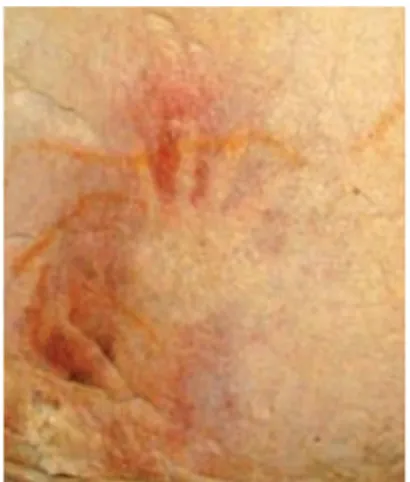
(18) Thèse de Ilias Sourikopoulos, Lille 1, 2015. Chapter 1 Introduction Our very existence relies on communication. We receive information from the environment through our senses and at the same time we emit ourselves, consciously or not, by action or emotion. We establish inter-personal relations and have evolved our societies. We use codes to get through and we continue to nurture and evolve them. Our reach has extended. We have cooperated to surpass the inhibiting constraints of our biological limits and we continue to build wonders. Our voices and images now resonate across the planet as we probe our cosmos to find meaning. Audiovisual information has been the most comprehensive for our understanding and has been communicated since the depths of time. Unfortunately, for audio, it took a great deal of human evolution to reach the invention of phonautograph1 (Figure 1-1) [Crandall, 1925]. This explains the profound lack of empirical data on the age and origin of language and the apparent debate of theories on language evolutionary models [Ulbaek, 1998]. On the other hand, visual information has been carefully preserved for us to find under thin layers of calcite. Hand stencils (Figure 1-2) in the El Castillo cave in Spain mark among the oldest findings of prehistoric painting dating at least 37000 years ago [Pike, 2012]. This is perhaps the first proof of abstract thinking, symbolism or even art. We are still trying to reconnect with the messages of our ancestors to define who we are.. Fig. 1-1. The first phonautograph.. 1Invented. Fig. 1-2. A 37.000 year old “hello world”.. by the Parisian inventor Edouard-Leon Scott de Martinville in 1857. 18 © 2015 Tous droits réservés.. doc.univ-lille1.fr.
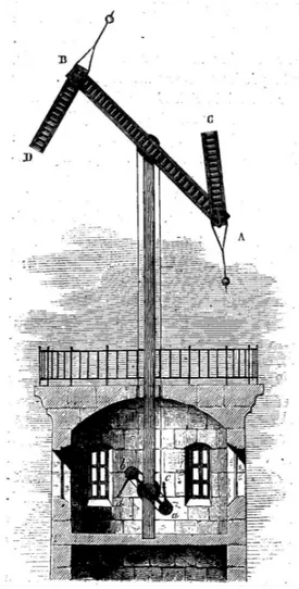
(19) Thèse de Ilias Sourikopoulos, Lille 1, 2015. The need to relay messages in distance spawned to define what we call today telecommunications2. The societies grew in numbers and populations spread geographically. The scope increased and became of great importance in administration, as well as in times of war. Information based on pre-agreed codes and arrangements has been transmitted and received from ancient times using fire and smoke. In the tragic trilogy Oresteia [Aeschylus, 458BC], it is mentioned that the message for the fall of Troy was relayed back to Mycenae by mountain-top fire beacons (φρυκτούς). The exact position of the beacons is recited, covering mostly over-sea distance of hundreds of miles. A similar example of communication included the use of smoke signals over the Great Wall of China [Sterling, 2008]. These can be described today as examples of a 1-bit Line-ofSight communication with coding. Lots of techniques as such have been used in the pre-electric era to achieve long distance relays. As a precursor to the. postal. service,. couriers. or. messengers on horseback, or running, relayed the vital information. In the romantic. example. of. Browning’s. poem, Pheidippides, the eponymous runner is depicted as the bearer of news of the Athenian victory in the battle of Marathon. In a more recent example, in 18th century France, methods of messaging included. notably. the. telegraph. semaphore, which is a visual longdistance sign system used during Napoleonic times (Figure 1-3) and the heliographs: the solar light flashing. Fig. 1-3. “Télégraphe de Chappe” named after the inventor.. system which was still used in the 20th century. With the evolution of electromagnetic theory by a number of scientists around the end of the compound of the Greek prefix tele- (τηλε-), meaning "distant", and the Latin communicare, meaning "to share" conceived by the French engineer and novelist Édouard Estaunié.. 2. 19 © 2015 Tous droits réservés.. doc.univ-lille1.fr.
(20) Thèse de Ilias Sourikopoulos, Lille 1, 2015. 19th century, electricity, wired and wireless telecommunications were established. The first electric telegraph line was set in 1844 between Washington and Baltimore. In 1876 the telephone was presented by Bell and in 1887 the transmission of electromagnetic waves was demonstrated by Hertz. The turn of the century found many scientists and entrepreneurs capitalizing on the scientific achievements and striving to advance the technology of electronic components. Up to now, little has changed in regard to the momentum of this movement. This continuous effort is constantly changing multiple aspects of our everyday life, from communications and healthcare, to commerce, education and entertainment. This thesis joins this effort. The work carried out is aiming to be applied to high-speed (Gb/s) communications by virtue of millimeter wave (mm-Wave) wireless transmission. In the rest of this introduction we highlight the main influencers of this work, namely, mmWave communications, circuit design with FD-SOI technology, and continuous-time digital signal processing. These will lead to stating the contribution of this thesis. The chapter ends by outlining the organization of this manuscript.. 1.1 A gun that fired 100 years later In March 6, 1899 Lord Rayleigh communicated to the Royal Society in London the results of experiments by Jagadish Chandra Bose, who was performing millimeter-wave research and had invented a novel detection device. Bose had also developed multiple components to accommodate millimeter wave transmission [Sen, 1997] including a millimeter wave spark transmitter and the abovementioned self-recovering coherer detector. All these were used in a demonstration of remotely firing a gun. According to [Bondyopadhyay, 1998] which attempts to correct a “century-old misinformation”, it is J.C Bose who is responsible for the “mercury coherer with a telephone” that G. Marconi used for the transatlantic radio transmission in 1901, while Marconi’s patent features a trivially modified version of Bose’s detector. Almost a century later (in 1994), the United States Federal Communication Commission (FCC) put mm-Wave research on the map by establishing an unlicensed band at 59-64GHz. Soon, multiple regulatory bodies around the world allocated overlapping bands. For instance, in Europe and Japan the 57-66GHz band was allocated. The 9GHz bandwidth was partitioned by the International Telecommunication Union [ITU] into four channels of 2.16GHz starting. 20 © 2015 Tous droits réservés.. doc.univ-lille1.fr.
(21) Thèse de Ilias Sourikopoulos, Lille 1, 2015. an era of Gb/s wireless data rates. As mentioned, applied research in millimeter-wave communications dates back to the turning of the last century. Nevertheless, a center stage role was taken for the last 20 years, promptly following regulation. Around the early 1990s, the first efforts in building radios around the 60GHz band were targeting III-V semiconductors [Niomiya, 1996], because their inherent characteristics enable high frequency operation. However, as shrinking of the transistor sizes went on, and cut-off frequencies increased, silicon CMOS adoption was pursued, notably from the 130nm node [Razavi, 2006]. A comprehensive summation of the state of the art in 60GHz integrated circuits and systems can be found in [Rappaport, 2011]. As far as standardization is concerned, the preliminary work of Task Group 3c on IEEE 802.15 soon evolved and currently mm-Wave communications are identified in the IEEE 802.11ad-2012 amendment as the forthcoming generation of Wireless Local Area Networks. Though products and dedicated solutions have been primarily presented by the television manufacturers of the WirelessHD consortium [WiHD], it is expected that full commercial adoption of the technology will be triggered by the computer manufacturers’ alliance. Indeed, recently, the standard has been promoted by merging the so-called WiGig Alliance with the Wi-Fi Alliance [Wi-Fi, 2013]. With unique standardization and marketing put in place, major computer and chip manufacturers are expected to populate the first generation of consumer products very soon. Mm-Wave communications are currently taking off. At this opportune timing, this thesis work encompasses mm-Wave communications as the application field. It focuses in mobile device integration, which is expected to take some more time to be deployed commercially, due to overhead software development and power consumption issues.. 1.2 The never ending revolution Since the achievements of the pioneers in the beginning of the last century, an ever growing torrent of scientific advancement is turning science-fiction to reality. From the days of the radio and the transmission of sound, we have gone to satellites, the internet, and ubiquitous connectivity. The transmission of image and sound with unprecedented definition is common in our modern systems. Nonetheless, nanotechnology is promising to extend the information exchange to concerning more senses in the next few years [Toko, 2013]. This relentless boom of technology has been mainly fueled by augmenting information processing capabilities.. 21 © 2015 Tous droits réservés.. doc.univ-lille1.fr.
(22) Thèse de Ilias Sourikopoulos, Lille 1, 2015. Fig. 1-4 FD-SOI transistor cross-section [STMicro].. Set off by the invention of the integrated circuit, the miniaturization efforts have gone the distance from microns to nanometers in a scaling frenzy. Processing power doubled every couple of years and promptly rendered relatively any “new” technology soon obsolete. The circuit design workhorse radically changed our way of living; the way we communicate and the way we process information. Throughout this scaling process, though multiple innovations have been applied over the years to address the physical phenomena encountered, the principle of operation for the transistor devices has remained the same. As this thesis is written, transistor sizing in production has reached 14nm. The involved phenomena of short-channel effects (SCE) and drain induced barrier lowering (DIBL) [SOI, 2014] have pushed major manufacturers to diverge from the typical bulk CMOS paradigm in order to ensure continuing shrinking device size unobstructed. At the time, bulk CMOS is been replaced by process methodologies as 3D Tri-gate [Intel, 2015], FinFet [TSMC, 2015] or FDSOI [STMicro], concerning high-end nodes below 32nm. For the prototyping purposes of this thesis 28nm Fully Depleted Silicon over Insulator (FDDOI) offered by STMicroelectronics was available. FD-SOI features a very thin un-doped silicon film implementing the transistor channel. Beneath the channel, a buried thin body oxide is developed, as shown in Figure 1-4, which effectively enables modulation of the transistor threshold by regulating the voltage on the transistor body. The body biasing option serves effectively as a knob in optimizing performance and power. When the polarization of the substrate is positive, as in creating the same field direction as the gate (Forward Body Bias), the transistor can be switched faster. As it will be seen further, being able to work upon this technology enabled unique research directions for this work.. 22 © 2015 Tous droits réservés.. doc.univ-lille1.fr.
(23) Thèse de Ilias Sourikopoulos, Lille 1, 2015. 1.3 All is digital, but what about timing? The term “digital system” is very commonly used not only to describe how a system processes information, but also to imply the system’s timing characteristics. This is because most digital systems operate in the discrete-time domain. However, demonstrated continuous-time digital signal processors (CT-DSP) [Kurchuk, 2012] [Vezytzis, 2015] propose digital data processing without the use of a clock reference. This enables unique performance characteristics. In clocked systems, processing operations go on even in the absence of the input signal. In CT-DSP, it is the presence and dynamic characteristics of that signal that essentially drive the processing of data. It has been proven that this leads to activity dependent power consumption and a less noisy spectral output, because the absence of sampling mitigates the presence of quantization noise. The main features of this methodology are notably level-crossing quantizers and continuoustime digital delay elements in order to implement digital filters similar to the one seen in Figure 1-5. During this thesis the design of continuous-time delay elements has been undertaken using ideas from the works that followed this principle.. Fig. 1-5 Continuous-time digital signal processor block diagram [Tsividis, 2006].. 23 © 2015 Tous droits réservés.. doc.univ-lille1.fr.
(24) Thèse de Ilias Sourikopoulos, Lille 1, 2015. 1.4 Thesis contribution As the aforementioned fields fused during the time of this thesis, the research results, demonstrated through this manuscript, are the following: •. An approach dealing with the problem of baseband equalization in mm-Wave communications. Line-of-Sight (LOS) deployment is suggested in order to motivate the development of low-power equalization for mobile devices. An efficient criticaltap cancellation scheme is proposed, which entails digital filtering implemented with variable coefficients in magnitude as well as delay. The use of continuous-time delays is considered, in order to mitigate overhead consumption due to clock routing and establish a channel dependent power consumption profile [Sourikopoulos, 2014].. •. The design of a tunable digital continuous-time delay element in 28nm FD-SOI. The introduction of body-biasing is attempted for the first time in developing such circuits in order to validate the fact that gate/body biasing can enable a coarse/fine control scheme for the output delay value.. •. The design of a flexible low-power mixed-signal decision feedback equalizer for 60GHz channels in 28nm FD-SOI. The topology features multiple continuous-time delay lines composed of the aforementioned delay elements. The results reveal that the power consumption of this circuit: (i) is lower than traditional implementation with clocked elements and (ii) depends on the channel realization targeted for equalization.. 1.5 Thesis organization The remainder of this manuscript is organized as follows: Chapter 2 is a crash course in 60GHz channel equalization. The problem of Inter-Symbol Interference (ISI) is elaborated and the different approaches in equalization are iterated along with the state of the art. Chapter 3 describes our proposed approach in the context of mixed-signal equalization. The theoretical/simulated results presented here have motivated the prototyping work. Chapter 4 deals with the design of the proposed delay element. After going through relevant state of the art and simulated results, silicon prototyping for a delay line is detailed and. 24 © 2015 Tous droits réservés.. doc.univ-lille1.fr.
(25) Thèse de Ilias Sourikopoulos, Lille 1, 2015. measurement results are presented. Chapter 5 presents the design of the proposed equalizer. It highlights key design choices and concludes with the demonstration of the characterization test-bench and measurement results. Chapter 6 concludes this manuscript by reflecting on the outcome of this effort and proposing directions for further research.. 1.6 Chapter Bibliography [Aeschylus, 458BC] Aeschylus - Agamemnon, verses 280-330 [Bondyopadhyay 1998] Bondyopadhyay, P.K. “Sir J.C. Bose Diode Detector Received Marconi’s First Transatlantic Wireless Signal of December 1901 (the ‘Italian Navy Coherer’ Scandal Revisited).” Proceedings of the IEEE 86, no. 1 (January 1998): 259–85. doi:10.1109/5.658778. [Crandal, 1925] Crandall, Irving B. “The Sounds of Speech.” Bell System Technical Journal 4, no. 4 (October 1925): 586–626. doi:10.1002/j.1538-7305.1925.tb03969.x. [Intel, 2015] “Intel®22 nm Technology.” http://www.intel.com/content/www/us/ en/silicon-innovations/intel-22nm-technology.html. [ITU] ITU: Committed to Connecting the World.” http://www.itu.int/en/Pages/default.aspx. [Kurchuk, 2012] Kurchuk, M., C. Weltin-Wu, D. Morche, and Y. Tsividis. “Event-Driven GHzRange Continuous-Time Digital Signal Processor With Activity-Dependent Power Dissipation.” IEEE Journal of Solid-State Circuits 47, no. 9 (September 2012): 2164–73. doi:10.1109/JSSC.2012.2203459. [Ninomiya, 1996] Ninomiya, T., T. Saito, Y. Ohashi, and H. Yatsuka. “60-GHz Transceiver for High-Speed Wireless LAN System,” 2:1171–74. IEEE, 1996. doi:10.1109/MWSYM.1996. 511238. [Pike, 2012] Pike, A. W. G., D. L. Hoffmann, M. Garcia-Diez, P. B. Pettitt, J. Alcolea, R. De Balbin, C. Gonzalez-Sainz, et al. “U-Series Dating of Paleolithic Art in 11 Caves in Spain.” Science 336, no. 6087 (June 15, 2012): 1409–13. doi:10.1126/science.1219957.. 25 © 2015 Tous droits réservés.. doc.univ-lille1.fr.
(26) Thèse de Ilias Sourikopoulos, Lille 1, 2015. [Rappaport, 2011] Rappaport, T.S., J.N. Murdock, and F. Gutierrez. “State of the Art in 60-GHz Integrated Circuits and Systems for Wireless Communications.” Proceedings of the IEEE, vol. 99, no. 8 (August 2011): 1390–1436. doi:10.1109/JPROC.2011.2143650. [Razavi, 2006] Razavi, B. “A 60-GHz CMOS Receiver Front-End.” IEEE Journal of Solid-State Circuits 41, no. 1 (January 2006): 17–22. doi:10.1109/JSSC.2005.858626. [Sen, 1997] Sen, A.K. “Sir J.C. Bose and Radio Science,” 2:557–60. IEEE, 1997. doi:10.1109/MWSYM.1997.602854. [SOI, 2014] Kononchuk, Oleg, and Bich-Yen Nguyen, eds. Silicon-on-Insulator (SOI) Technology: Manufacture and Applications. Woodhead Publishing Series in Electronic and Optical Materials 58. Amsterdam: WP, Woodhead Publ./Elsevier, 2014. [Sourikopoulos, 2014] Sourikopoulos, Ilias, Antoine Frappe, Andreas Kaiser, and Laurent Clavier. “A Decision Feedback Equalizer with Channel-Dependent Power Consumption for 60GHz Receivers,” International Symposium in Circuits and Systems, Melbourne, Australia 1484– 87. IEEE, 2014. doi:10.1109/ISCAS.2014.6865427. [Sterling, 2008] Sterling, Christopher H., ed. Military Communications: From Ancient Times to the 21st Century. Santa Barbara, Calif: ABC-CLIO, 2008. [STMicro] http://www.st.com/web/en/about_st/fd-soi.html [Tsividis, 2006] Tsividis, Y. “Mixed-Domain Systems and Signal Processing Based on Input Decomposition.” IEEE Transactions on Circuits and Systems I: Regular Papers 53, no. 10 (October 2006): 2145–56. doi:10.1109/TCSI.2006.882822. [TSMC, 2015] “Taiwan Semiconductor Manufacturing Company Limited.” http://www.tsmc.com/english/dedicatedFoundry/services/reference_flow.htm. [Toko, 2013] Toko, Kiyoshi, Takeshi Onodera, and Yusuke Tahara. “Nano-Biosensors for Mimicking Gustatory and Olfactory Senses.” In Bio-Nanotechnology, edited by Debasis Bagchi, Manashi Bagchi, Hiroyoshi Moriyama, and Fereidoon Shahidi, 270–91. Oxford, UK: Blackwell Publishing Ltd., 2013. http://doi.wiley.com/10.1002/9781118451915.ch15. [Ulbaek, 1998] Ib Ulbaek: The origin of language and cognition. In Hurford, James R., ed. Approaches to the Evolution of Language: Social and Cognitive Bases. Repr. Cambridge: Cambridge Univ. Press, 2001. [Vezyrtzis , 2014] Vezyrtzis, C., W. Jiang, S.M. Nowick, and Y. Tsividis. “A Flexible, Event26 © 2015 Tous droits réservés.. doc.univ-lille1.fr.
(27) Thèse de Ilias Sourikopoulos, Lille 1, 2015. Driven Digital Filter With Frequency Response Independent of Input Sample Rate.” IEEE Journal of Solid-State Circuits Early Access Online (2014). doi:10.1109/JSSC.2014.2336532. [WiHD] http://www.wirelesshd.org/ [Wi-Fi, 2013] “Wi-Fi Alliance® and Wireless Gigabit Alliance to Unify | Wi-Fi Alliance.” http://www.wi-fi.org/news-events/newsroom/wi-fi-alliance-and-wireless-gigabit-allianceto-unify.. 27 © 2015 Tous droits réservés.. doc.univ-lille1.fr.
(28) Thèse de Ilias Sourikopoulos, Lille 1, 2015. Chapter 2 Connected within closed doors Thanks to the continuous effort to deliver ever higher information throughput, digital communications are at the doorstep of commercialization for the 60GHz era and multi-Gbps wireless transmission. Actively researched for more than 20 years, major stakeholder consortia now drive the industry towards what is a paradigm shift in wireless connectivity and Wi-Fi experience. This was sparked by putting this millimeter wave communication scenario on the map of regulatory bodies. After multinational coordination, 5GHz of continuous bandwidth worldwide have been made available for general use (industrial, medical and scientific) wireless and mobile communications. Wide adoption for this technology has set off by complementing current popular wireless and mobile standards. Major telecommunication companies and research institutions are grooming this technology for what will be 5G (or more for that matter) in the mobile evolution [Rappaport, 2013], while the standardization of a new 60GHz generation of Wi-Fi as in [802.11ad, 2012] has been in place already since late 2012. The first commercial transceiver chip along with the first personal computer featuring 60GHz technology have already been showcased and as major computer and telecommunication companies are beginning to get involved, wide proliferation is expected soon. A recent financial report [MarketsAndMarkets, 2015] forecasts a 1.7 billion market for 60GHz products in the next five years. Concerning the technical challenges, multiple innovations have enabled progress. Obviously the leap to the 60GHz band has introduced a series of challenges starting with front-end technology and this is due to the special characteristics of the wireless channel. During signal propagation, high attenuation and low diffraction effects are experienced. That’s why this technology largely depends upon the use of high gain antennas with beamforming to establish the communication link. The focus of this work aims at the baseband part of a 60GHz receiver, namely on the equalizer block. This block is responsible for the removal of Inter-Symbol Interference (ISI) after signal down-conversion. This chapter will provide a foundation for the contribution of this thesis. Key channel characteristics will precede the presentation of state of the art equalization methods and the. 28 © 2015 Tous droits réservés.. doc.univ-lille1.fr.
(29) Thèse de Ilias Sourikopoulos, Lille 1, 2015. evaluation of the equalizer in the receiver baseband chain. The mixed-signal equalization approach has been recently put forward as the most energy efficient one, so the chapter concludes with the presentation of state of the art of mixed signal DFEs. These developments will be the pilot to the essence of this research effort: the system and circuit level contributions presented in the chapters to follow.. 2.1 Communicating through the 60GHz channel Establishing a communication channel of 60GHz has revealed multiple intricacies that not only change drastically the relevant transceiver architecture front-ends and PHYs, but also propose new use-models for future systems. Generally, comparing with established standards in the 2-5GHz band, one can expect 20-30dB more attenuation, with a quasi optical character and building material confinement. Though these intricacies in channel modeling are out of the scope of this thesis, it is important for system architecture design to have insight into the main features of transmission. This will readily help identify the applicable communication scenarios and equipment for deployment. Therefore, as a foundation, basic features of propagation through the 60GHz channel are presented in this section.. 2.1.1 Free space loss and beamforming It is well known from electromagnetism that as frequencies of transmission increase, the capability of establishing a communication link demands more power. For 1 meter of free space propagation, according to [Friis, 1946], the 60GHz channel exhibits almost 28dB higher loss than the 2.4GHz channel. Apart from free space path loss, millimeter wave propagation accounts for extra attenuation due to atmospheric absorption by oxygen, water vapor or rainfall.. Figure 2-1 displays the attenuation of electromagnetic signals in air. These. conditions undermine any overall low power operation specification at the transceiver. That’s because for what concerns the most power hungry component of the system the power amplifier, more power is needed in order to compensate for the increased path loss. In addition to that, it also means less efficiency when comparing with a lower frequency transmission, because the amplifier is operating closer to the maximum frequency of operation. Evidently, this mode is not encouraging long distance communications. This. 29 © 2015 Tous droits réservés.. doc.univ-lille1.fr.
(30) Thèse de Ilias Sourikopoulos, Lille 1, 2015. Fig. 2-1 Average atmospheric absorption of millimeter waves [FCC, 1997 and Lai, 2008].. caused relaxing substantially the regulation for transmitted power. For example, in the United States, as per [FCCpart15, 2009], the limit for field strength in the 57-64GHz band is around 165 times the limit for emissions in the 2.4-5GHz band. This fact, however, has some positive ramifications as a communications scenario because interception becomes more difficult due to the weaker signal. This becomes attractive in terms of data security. In fact, 60GHz transmission was first proposed as a battlefield communications mode exactly for this reason [Agilent, 2013]. Furthermore, from a spectrum utilization standpoint, spectrum decongestion can be envisioned as the established link becomes easily spatially confined and still there’s ample bandwidth in comparison with the lower GHz bands. In order to compensate for the path loss, beamforming has been regarded as a key enabling. Fig. 2-2 Beamforming principle of operation [Ruckus, 2013].. 30 © 2015 Tous droits réservés.. doc.univ-lille1.fr.
(31) Thèse de Ilias Sourikopoulos, Lille 1, 2015. technology. Beamforming refers to using multiple antenna elements in order to enhance antenna directivity. The beamforming gain is realized by introducing a phase shift between the different antenna elements as seen in Figure 2-2. This results to the appearance of maxima in total radiated energy towards a certain direction, due to constructive interference. Therefore, signal power and consequently SNR are increased and faster data rates are achieved. This technique is more suited to millimeter-wave communication rather than the 2.4-5GHz band, because multiple antenna elements can occupy a smaller area. For example, a square 4x4 antenna array with 16 antenna elements could be packed in 1cm2 with adjacent elements separated by half the wavelength [Perahia, 2010].. 2.1.2 Penetration and reflectivity One of the most prominent facts about signal propagation at 60GHz is that it generally exhibits high penetration losses and generally poor reflectivity on common building materials. Some penetration losses from the literature, are presented in Table 2-I. Also, as mentioned in [Maltsev, 2014], propagation through diffraction is a practically unviable mechanism. The power transmitted reaches the receiver through the Line-Of-Sight or signal reflections as seen in Figure 2-3. The latter are expected to sustain substantial attenuation depending on the reflectivity of the material. As derived from the measurements of. Fig. 2-3 3D model of conference room highlighting reception through 1st and 2nd order reflections from the ceiling and walls [Maltsev10].. 31 © 2015 Tous droits réservés.. doc.univ-lille1.fr.
(32) Thèse de Ilias Sourikopoulos, Lille 1, 2015. Table 2-I Typical penetration losses [Xu 2002], [Manabe 1996], [Sato, 1997], [Langen, 1994].. Building Material Penetration Loss Glass. 1.7-4.5 dB. Plasterboard Wall. 5.4 to 8.1 dB. Wooden panel. 7 dB. Limestone. >30 dB. Concrete. >30 dB. Metalized glass. >30 dB. Granite. >30 dB. [Langen, 1994], reflectivity is associated with the thickness as well as the roughness of the material surface and could reach a few decades of decibels from common building materials. Therefore, it is expected that for indoor environments, the practical use model will be receiving the signal from the direct path, or worse, by locking-in to a low-order reflection (i.e. after one or two consecutive interactions with the surroundings). The latter will demand a more austere link budget. For this reason, in order to minimize losses, the antenna beam should be steered towards the transmitter or the point of reflection.. 2.1.3 Multipath propagation and Inter-Symbol Interference With the previous descriptions we can surmise that the power reaching the receiver will be the sum of radiation coming from different directions. This multipath propagation is a general characteristic of wireless channels and refers to the existence of a multitude of propagation paths from the transmitter to the receiver. The signal can be reflected, diffracted or scattered along its way [Molisch, 2011]. Already, it is clear that signal propagation in 60GHz might appear spatially confined, especially when indoors, so a large number of multipath components (essentially echoes of the signal) might arrive at the receiver. These components, following different trajectories, arrive at the receiver with different delay times. The extent of these arrivals in time constitutes the delay spread of the channel.. 32 © 2015 Tous droits réservés.. doc.univ-lille1.fr.
(33) Thèse de Ilias Sourikopoulos, Lille 1, 2015. Fig. 2-4 Multipath propagation and channel impulse response from [Molich, 2011]. Echoes of the signal arrive through different paths spreading the channel impulse response in time.. We can instantiate exactly this situation by taking a snapshot of the amplitude and phase of the received components after transmitting an impulse to provide the channel impulse response realization (IR throughout this text) as seen in Figure 2-4. In an ideal channel case the response should be a single impulse, however, what we have is a series of multipath components corresponding to the different propagation paths, as depicted. These multipath components are the result of scaling and phase shifting of the original impulse, sustained throughout propagation. If there is visual contact between the receiver and the transmitter, the maximum amplitude component will refer what is known as the LOS path, which arrives always first ahead of all others. This is because it covers the shortest distance and sustains minimum interaction with the environment. In a situation where no visual contact is established, the highest amplitude component will refer to the most powerful reflection, due to the signal bouncing off a reflective surface. In any of these two cases, this component represents the reference with which the receiver will synchronize. This component is called the cursor. In the case of receiving a symbol, if the delay spread is longer than symbol duration, then Inter-Symbol Interference is observed, which potentially leads to the loss of data. Figure 2-5 details the situation. A data stream is sent by the transmitter (Tx) in the top waveform. The data propagate through the multipath channel and arrive arbitrarily scaled, delayed and dephased to the transmitter. The examples of three path waveforms are displayed.. 33 © 2015 Tous droits réservés.. doc.univ-lille1.fr.
(34) Thèse de Ilias Sourikopoulos, Lille 1, 2015. Fig. 2-5 Demonstrating ISI generated by the superposition of three components at the receiver input [Molisch, 2011].. These arriving waveforms, noted as Paths 1-3, are summed at the receiver. Upon reception the receiver should take a decision about the symbol arriving. The simplest way is applying an amplitude threshold for comparison. So, as the amplitude of the received symbol is compromised by interfering symbols, the decision could be erroneous, resulting in data loss. The use of directive antennas and beamforming, however, shortens the delay spread because it permits only a part of the multipath spread to arrive with sufficient power to the receiver. Unfortunately, in the case of the 60GHz channel, as seen in all experimental results, [eg. Xu, 2002] multiple decades of nanoseconds of multipath spreads are expected for common indoor environments (living room, conference room, cubicle) even with applied beamforming transmitter and receiver. ISI is the cause of irreducible errors that cannot be remedied by simply increasing the power in the transmitter. Therefore, dedicated functions are needed to confront the situation. These measures can be the application of OFDM (Orthogonal Frequency-Division Multiplex) or the employment of equalizers. We will review these further, after summarizing some channel modeling aspects.. 34 © 2015 Tous droits réservés.. doc.univ-lille1.fr.
(35) Thèse de Ilias Sourikopoulos, Lille 1, 2015. Fig. 2-6 60GHz channel impulse response structure from [Maltsev, 2014].. 2.1.4 Features of channel modeling Despite the fact that the impulse response is sufficient to describe the behavior of linear and time invariant systems, this is not the case for a 60GHz channel. As already mentioned in the previous paragraph, we refer to impulse response realizations to hint the fact that the communication channel is dependent on the environment. It is commonly modeled as a linear time variant system to reflect relatively fast changes in the environment, like for instance the case of mobility. Analyzing the different impairments that the signal undergoes in a deterministic way is usually complicated and renders little accuracy. So, most of the times, the goal is to describe the probability of attaining a value for a certain parameter. This is done through assigning the description of related phenomena to statistical distributions. For instance, the Rayleigh and the Rician distributions are used to describe the fluctuations for multipath fading in the 60GHz channel [Molisch, 2011]. Besides the multipath character, the 60GHz channel has also been reportedly exhibiting a clustered impulse response structure seen in Figure 2-6. In an ideal reflection case one ray associated with the reflection should be received. However, the multipath components referring to reflection paths appear to form clusters. In studies of channel characterization experiments [Sawada, 2010] clustering has been attributed to the fine character of reflecting surfaces. Statistic distributions are employed to intra and inter-cluster characteristics such as. 35 © 2015 Tous droits réservés.. doc.univ-lille1.fr.
(36) Thèse de Ilias Sourikopoulos, Lille 1, 2015. cluster amplitude and timing. Total signal amplitude may vary because of shadowing from objects preventing the signal to reach the receiver, or even slight movement. For a better understanding of what the latter entails, a movement of the receiver for a few millimeters might turn interference from constructive to destructive for the 60GHz band. In the case of 2GHz that could have been around 10cm. Additionally, when signal propagation is blocked, some components from the impulse response could be either removed or even more clusters could be added, because of additional reflections. This effect is taken into account by the introduction of the cluster blockage probability associated with each type of cluster. Another key point is that the channel has been verified by multiple measurements to have a quasi-optical nature. For this reason ray-tracing can be employed as a technique to predict the channel behavior and aid in spatial and temporal modeling [Maltsev, 2014]. In addition to the above, propagation has been sensitive to antenna polarization mismatches between the receiver and transmitter. Polarization is a property of EM waves describing the orientation of the electric field and magnetic intensity in space and time. Experimental proof of the strong polarization impact on 60 GHz WLAN systems was given in [802.11ad_model, 2010]. In [Maltsev, 2010] scenarios with losses as large as 10-20dB are attributed to polarization mismatches. The most robust arrangement was measured when horizontal polarization is used in the transmitter and circular in the receiver (or vice versa). This approach minimizes the degradation due to polarization mismatch to moderate values (2–3 dB).. 2.1.5 Simulating 60GHz channels Models for simulation of communication over the 60GHz band have been recently available under the auspices of the standardization efforts for the 802.15.3c Wireless Personal Area Networks (WPANs) [TG3c, 2009] as well as the 802.11ad Wireless Local Area Networks (WLAN) [TGad_model_doc, 2010]. Though throughout this thesis both models have been used for simulation, the results presented in this and later chapters have been produced with the release of the 802.11ad model, which was issued during this thesis work period and is considered the state of the art for reference purposes.. 36 © 2015 Tous droits réservés.. doc.univ-lille1.fr.
(37) Thèse de Ilias Sourikopoulos, Lille 1, 2015. Fig. 2-7 Impulse response realizations created by the 802.11ad model for a living room setting with (a1, a2) different Tx-Rx distance and (b1, b2) different Rx HPBW. The total power of all cluster rays is normalized to one.. In the 801.11ad model used for simulations [TGad_model, 2010] there are three available environment options: living room, cubicle and conference room. Prior to generating impulse responses a configuration file is set up. This file enables manual tuning of various parameters such as sampling rate, distance, probability of reflection blockers, antenna type and polarization. In Figure 2-7(a1, a2) the effect of distance is shown. As the distance increases, the cursor diminishes due to free space path loss. In the examples (b1, b2) the half-power beam-width (HPBW) is varied. With the smaller angle, spatial filtering is essentially performed, so energy reception from different directions due to reflection is close to zero.. 37 © 2015 Tous droits réservés.. doc.univ-lille1.fr.
(38) Thèse de Ilias Sourikopoulos, Lille 1, 2015. Fig. 2-8 Tapped delay line channel model in [Proakis, 2007].. In order to further investigate system performance a simulation test-bench is built, in which the channel is represented as a tapped-delay line. To emulate multipath propagation, the coefficients are set by the channel impulse response realizations coming from the [TGad_ model, 2010]. Variation of the Signal to Noise Ratio (SNR) is achieved by adding noise to the output3. This setup, displayed in Figure 2-8, was used to perform Bit Error Rate simulations and evaluate receiver performance.. 2.2 Equalization for 60GHz channel receivers Multipath fading is considered an irreducible error in signal transmission. This means that it cannot be mitigated by increasing transmit power or reducing receiver noise figure. So, the receiver should be built accordingly in order to combat the delay-dispersive environment that the 60GHz channel imposes. The measures taken usually are the appropriate choice of a modulation scheme or the use of equalization. Equalization in its most straightforward kind (the linear equalizer) involves the application of a filter in the receiver which aims at inverting the channel impulse response. Effectively, this. 3. This can be also carried-out by convolving with an Added White Gaussian Noise channel. 38 © 2015 Tous droits réservés.. doc.univ-lille1.fr.
(39) Thèse de Ilias Sourikopoulos, Lille 1, 2015. A. A. ZF equalizer. MMSE equalizer. channel. channel. f. f. Fig. 2-9 By applying an MMSE criterion the error between the transmitted signal and the output of the equalizer is minimized.. removes all impairments that stem from the channel. The situation, however, complicates with the presence of noise. As shown in Figure 2-9, when compensating for a fade, applying exactly the inverse transfer function will actually amplify any noise as well. This is known as the zero forcing (ZF) criterion. The situation worsens when frequency nulls are present: an inverting filter will amplify noise to the maximum [Proakis, 2007]. A solution is to apply a minimum mean square error (MMSE) criterion. This will effectively minimize the noise contribution at the receiver, rather than trying to totally dismiss ISI by inverting the channel. Equalization can be either performed in the time or the frequency domain. Time-domain implementations using mixed-signal design have been recently suggested as a low power solution suitable for mobile terminal integration in 60GHz systems [Sobel, 2009]. In the rest of this section, after reviewing generally equalization and reflect on system integration in terms of system power consumption, we will revise the relevant state of the art in mixed signal equalization.. 2.2.1 OFDM and Frequency domain equalization Dealing with the effect of the channel multipath and ISI in the receiver can be simply done by lowering the data rate. This would require establishing a symbol duration that is substantially longer that the delay spread of the channel. The transmitted symbol would then last longer than the effect of its last echo. This way the distorting effect of this echo would only affect the symbol currently transmitted and not any other. To bring some insight, let us visualize the eye diagrams in Figure 2-10 coming from three cases: (i) no. 39 © 2015 Tous droits réservés.. doc.univ-lille1.fr.
(40) Thèse de Ilias Sourikopoulos, Lille 1, 2015. Fig. 2-10 Eye diagram with (i) no multipath distortion (ii) one path arriving within symbol time (iii) one path arriving one symbol time later than the previous case.. interference (ii) one single echo sized 0.3x the cursor arriving during symbol time, and (iii) one single echo arriving one symbol time later. Distortion by components within symbol time might alter the eye shape, but still a simple shift in the decision phase could maximize performance. Things aren’t that straightforward with inter-symbol interference in case (iii). The cumulative effect of multiple paths contributing to the distortion will cause the eye to completely shut. Extra countermeasures need to be taken then, that is, dedicated equalizers. After following the above, it is easy to understand that schemes with multiple carriers that inherently use long symbol times in order to achieve multiplexing are resistant to the effect of multipath propagation. The known drawbacks, however, have to do with the power consumption. OFDM is costly on the transmitter power amplifier due to its high Peak to Average Power Ratio. Additionally, it assumes more complex processing on the digital baseband than simpler, single carrier schemes. In the work of [Mitomo, 2012] 320mW of power are needed for the OFDM/QPSK digital baseband implementing a 64-point I/FFT block for a short range/one-to-one transceiver design. A similar proximity transceiver demonstrated in [Saigusa, 2014], integrates a low 16-point I/FFT reporting a total of 125mW for the baseband. Nonetheless, by combining OFDM and very short distance links, the 60GHz channel multipath is substantially reduced and the need for elaborate equalization schemes is obviated. On the contrary, when choosing to apply a single carrier modulation scheme, to benefit from the less stringent linearity constraints in the front-end, frequency domain equalization is a. 40 © 2015 Tous droits réservés.. doc.univ-lille1.fr.
(41) Thèse de Ilias Sourikopoulos, Lille 1, 2015. Fig. 2-11 Principle of a SC-FDE linear equalizer as seen in [Saito, 2013].. choice that can actually coexist with OFDM. Single Carrier Frequency Domain Equalization (SC-FDE) is delivering similar performance to that of an OFDM system with essentially equivalent complexity [Falconer, 2002]. However, the power amplifier of an SC transmitter requires a smaller linear range to support an average power. This is why in mobile radios (LTE), the common practice is to use OFDM for the downlink and SC-FDMA on the uplink, in order to save battery power. [Korhonen, 2014]. The principle of a linear, frequency domain equalizer is presented in Figure 2-11. The aim to invert the channel’s frequency response is implemented in the frequency domain, so Table 2-II State of the art Frequency Domain Equalizers. Process [nm] Symbol Rate [GS/s] FDE [GS/s] Core clock [MHz] FFT IFFT Gate count (Data path) Gate count (Channel Est.) Power (Data path) [mW] Max. excess [ns]. [Saito, 2013] 40 1.76 3.52(x2 O.S) 220. [Hsiao, 2011] [Yeh, 2011] 65 65 1.76 1.76 1.76 1.76 440 330. 128pt (50%overlap). 512pt. 512pt. 64 pt 284k 403k 116 18. 512pt 522k 76k 208 36. 512pt 1723k 211 36. 41 © 2015 Tous droits réservés.. doc.univ-lille1.fr.
(42) Thèse de Ilias Sourikopoulos, Lille 1, 2015. an FFT is performed on the received signal and the output is scaled accordingly to perform the inversion. This is followed by an inverse FFT operation to return to the time domain and detect the symbol. State of the art FDEs are summarized in Table 2-II. The SC-FDE equalizer in [Hsiao, 2011] consumes 208mW with 7Gbps and 16QAM, while in [Saito, 2013] for the same rate the FDE consumes 116 mW.. 2.2.2 Time domain equalization Time domain equalization on the receiver side involves cancelling the channel echoes by directly filtering incoming symbols. In Figure 2-12 a linear time-domain equalizer is seen, which is implemented as an FIR filter. Usually filters as such work with symbol time delays (Symbol Spaced Equalizer). The channel is non-static, so the coefficients, bi(k), are variable and follow the channel changes. This is usually done by interposing a training mode, which sets the coefficients by comparing incoming data with a pilot, i.e. a priori known data. By using an adaptation algorithm the coefficients are periodically updated in order to follow the channel changes. Traditionally this kind of equalization has been regarded as inefficient when having to deal with the long delay spreads that are common in broadband wireless communications.. Fig. 2-12 Time-domain linear equalizer diagram from [Boccuzzi, 2008].. 42 © 2015 Tous droits réservés.. doc.univ-lille1.fr.
Figure
![Fig. 1-4 FD-SOI transistor cross-section [STMicro].](https://thumb-eu.123doks.com/thumbv2/123doknet/3741262.112535/22.892.330.658.110.308/fig-fd-soi-transistor-cross-section-stmicro.webp)
![Fig. 2-5 Demonstrating ISI generated by the superposition of three components at the receiver input [Molisch, 2011]](https://thumb-eu.123doks.com/thumbv2/123doknet/3741262.112535/34.892.212.777.112.545/fig-demonstrating-generated-superposition-components-receiver-input-molisch.webp)
+7
![Fig. 2-6 60GHz channel impulse response structure from [Maltsev, 2014].](https://thumb-eu.123doks.com/thumbv2/123doknet/3741262.112535/35.892.222.774.109.405/fig-ghz-channel-impulse-response-structure-maltsev.webp)
![Fig. 4-2 Programmable delay line in [Li, 2006].](https://thumb-eu.123doks.com/thumbv2/123doknet/3741262.112535/71.892.341.710.104.322/fig-programmable-delay-line-in-li.webp)
![Fig. 4-8 Schmitt trigger output stage on current starved delay from [Mahapatra, 2002]](https://thumb-eu.123doks.com/thumbv2/123doknet/3741262.112535/74.892.310.713.785.1056/schmitt-trigger-output-stage-current-starved-delay-mahapatra.webp)
![Fig. 4-10 Complete thyristor delay element with static triggering in [Kim, 1996].](https://thumb-eu.123doks.com/thumbv2/123doknet/3741262.112535/76.892.263.709.102.322/fig-complete-thyristor-delay-element-static-triggering-kim.webp)
![Fig. 4-12 Delay element in [Kurchuk, 2012].](https://thumb-eu.123doks.com/thumbv2/123doknet/3741262.112535/77.892.197.776.643.983/fig-delay-element-in-kurchuk.webp)
Documents relatifs
Ajouter une question à cocher de votre choix et faites en sorte que la case "Vous avez choisi la spécialité NSI soit cochée par défaut". Intro HTML / CSS : Travail sur
For instance, 13 designed a state feedback control law and a state observer for the one-phase Stefan problem by introducing a nonlinear backstepping transformation for moving
To account for the noisy nature of the data, we propose to use a statistical analysis method, the principal components analysis (PCA), to identify primitives from the
The role of the phase noise of a local oscillator driving a pulsed-mode RADAR used for probing surface acoustic wave sensors is investigated. The echo delay, representa- tive of
A strategy for generating high resolution time delays while allowing for long interrogation durations up to 5 µs is implemented by combining an FPGA-based delay generator
This paper is dedicated to the stability analysis of a class of uncertain distributed delay systems, the kernel of which can be modeled as a polynomial function of the delay..
differential equation (FDE) to that of the ordinary differential equa- tion (DE ) , propagation in the sense of the following
In the case of signed conjunctive queries (SCQ), where atoms could be negated, under a suit- able notion of acyclicity (somewhere between α-acyclicity and β-acyclicity) the
