HAL Id: hal-01343434
https://hal.archives-ouvertes.fr/hal-01343434
Submitted on 8 Jul 2016
HAL is a multi-disciplinary open access archive for the deposit and dissemination of sci-entific research documents, whether they are pub-lished or not. The documents may come from teaching and research institutions in France or abroad, or from public or private research centers.
L’archive ouverte pluridisciplinaire HAL, est destinée au dépôt et à la diffusion de documents scientifiques de niveau recherche, publiés ou non, émanant des établissements d’enseignement et de recherche français ou étrangers, des laboratoires publics ou privés.
Low Frequency Noise Of AlGaN/GaN HEMT Grown
On Al2O3 , Si And SiC Substrates
Jean-Guy Tartarin, Geoffroy Soubercaze-Pun, Abdelali Rennane, Laurent
Bary, S Delage, Robert Plana, Jacques Graffeuil
To cite this version:
Jean-Guy Tartarin, Geoffroy Soubercaze-Pun, Abdelali Rennane, Laurent Bary, S Delage, et al.. Low Frequency Noise Of AlGaN/GaN HEMT Grown On Al2O3 , Si And SiC Substrates. 18th International Conference on Noise and Fluctuations (ICNF 2005), Sep 2005, Salamanque, Spain. �10.1063/1.2036754�. �hal-01343434�
Low Frequency Noise Of AlGaN/GaN HEMT
Grown On Al
2O
3, Si And SiC Substrates
J.G Tartarin1-2, G. Soubercaze-Pun1-2, A. Rennane1-2, L. Bary1, S. Delage3, R. Plana1-2, J. Graffeuil1-2
1- LAAS-CNRS, 7 av. du Colonel Roche, 31077 Toulouse cedex 4, France 2- Université Paul Sabatier, 118 rte de Narbonne, 31062 Toulouse cedex 4, France
3- TRT-TIGER, domaine de Corbeville, 91404 Orsay cedex, France
Abstract. The use of wide bandgap materials for broadcast telecommunication and defense
systems allow high power, high efficiency and high integration levels of active devices thanks to their microwave electrical performances. GaN based devices have also demonstrated great potential for high frequency linear low noise applications. However, low frequency noise (LFN) performances characteristics are still under progress as they are related to the material quality and process control. As a consequence, the LFN sources identification and modeling in AlGaN/GaN devices have a twofold stake: on one hand it contributes to the process improvement by the identification of the main noise sources, and on the other hand the non-linear noisy model can be used for CAD of non non-linear circuits such as low phase noise oscillators. This study focuses on the confrontation of High Electron Mobility Transistors (HEMT) featuring 0.15x2x50µm² gate dimension grown by MOCVD on sapphire (Al2O3),
silicon (Si) and silicon carbide (SiC) substrates. Each substrate has got its own advantages and drawbacks in terms of cost, wafer size, thermal conductivity and lattice mismatch. This paper deals with the noise mechanisms relative to the use of several substrates: for that purpose, low frequency noise measurements have been performed under different biasing conditions for each substrate. The contributions of the different noise sources (1/f, generation-recombination centers (GR),…) are discussed for each substrate and related to each technological process.
Keywords: Low Frequency Noise, wide band-gap materials, SiC Si and sapphire substrates, G-R
centers, noise parameters extraction procedure.
PACS: 05.40.Ca, 73.50.Td, 85.30.De, 85.30.Tv
STATIC MEASUREMENTS
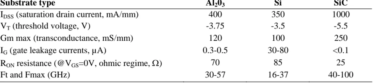
The HEMT devices grown on Silicon, silicon carbide and sapphire substrates have been processed using the same masks set. The Aluminum content in the 2 dimension Electron Gaz (2DEG) layer ranging from 22% to 24% according to the process is however close whatever the substrate. The MOCVD technique has been used for devices grown on sapphire and silicon carbide [1] while the MBE technique has been applied for devices on Silicon [2]. Static and pulsed measurements have been largely performed using some 10 samples for each different gate geometry (length, width) to appreciate the scattering of the electrical performances over the wafer (and so the yielding of each process). The main parameters are reported on Figure 1 for devices featuring 0.15x2x50µm². Devices on SiC exhibit improved performances in terms of higher drain current, higher transconductance gain and lower gate leakage current as
well as reduced contact or channel resistance RON, thus proving a better process maturity. Moreover, a better yielding has been measured for the process on SiC substrate. The following study on low frequency noise performances has been performed on standard devices for each substrate.
TABLE 1. HEMT (2x0.15x50µm² gate area) static parameters (mm unit refers to the normalization
against the gate width of the devices).
Substrate type Al203 Si SiC
IDSS (saturation drain current, mA/mm) 400 350 1000
VT (threshold voltage, V) -3.75 -3.5 -5.5
Gm max (transconductance, mS/mm) 120 100 250 IG (gate leakage currents, µA) 0.3-0.5 30-80 <0.1
RON resistance (@VGS=0V, ohmic regime, Ω) 70 85 25
Ft and Fmax (GHz) 30-57 16-37 40-100
LOW FREQUENCY NOISE (LFN)
The experimental setup used is based on the transimpedance amplifier direct measurement technique which allows rapid LFN measurements from 10Hz to 100kHz.
The different spectral densities on the drain (SID) and gate (SIG) accesses can be
simultaneously characterized as well as their cross-correlation. From a previous study
on SID versus the gate width and gate length [3], we have found the main noise
contribution to occur in the active region (2DEG) under the gate when the device is
biased in its saturated IDS(VDS) zone. Neither the various complex noise mechanisms
revealed by SIG measurements, nor the cross-correlation will be described in this
paper. Only the SID spectral measurements will be discussed in the next paragraphs:
the correlation has been found to be null, and so SIG impacts lowly on the overall noise
in circuits such as oscillators. Moreover, we have developed an analytical extraction procedure (MatLab) to get the different noise parameters contributions (1/f and generation-recombination G-R centers, noise floor, …). Figure 1 illustrates the different extracted noise contributions for a HEMT on SiC substrate.
1E-18 1E-17 1E-16 1E-15 1E-14 1E-13 10 100 1000 10000 100000 1000000 Frequency (Hz) SID (A²/ Hz ) GR1 GR2 GR3 GR4 1/f
Measurement& Model
1E-18 1E-17 1E-16 1E-15 1E-14 1E-13 10 100 1000 10000 100000 1000000 Frequency (Hz) SID (A²/ Hz ) GR1 GR2 GR3 GR4 1/f
Measurement& Model
FIGURE 1. Extracted low frequency noise sources (0.25x2x75µm² HEMT @ VGS=-2V, VDS=16V)
The robustness of this procedure has been checked with analytical noisy spectra to ensure the uniqueness of the parameters convergence. More than 6 G-R centers, as
well as flicker noise and floor noise can be extracted over the considered frequency range. The extraction accuracy is just limited by the noise contribution weight in the overall noise (the weaker the noise contribution, the worse the accuracy).
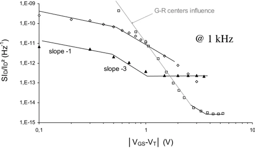
LFN Measurements - Linear Biasing Operating Mode
This study in the static IDS(VDS) Ohmic region allows the location and the
quantification of the dominating noise source that take place in the active 2DEG channel or in the contact resistances. The technique proposed by Peransin [4] is used in Figure 2. This method states that only flicker noise is taken into account.
1,E-15 1,E-14 1,E-13 1,E-12 1,E-11 1,E-10 1,E-09 0,1 1 10 G-R centers influence slope -1 slope -3 SI D /I D ² (H z -1 ) │VGS-VT│ (V) @ 1 kHz
FIGURE 2. LFNmeasured @ 1kHz (Ohmic region) according to Peransin’s technique applied to AlGaN/GaN HEMT featuring 0.15x2x50µm²: ▲ Al2O3, □ SiC, ◊ Si substrates
From the -1 slope for devices on Si and Al2O3 substrates (knowing the carrier
density and mobility), the Hooge parameters have been estimated respectively at
1,5.10-3 and 10-4. These results are coherent with the higher dislocations in the 2DEG
for device grown on silicon than on sapphire, mainly attributed to higher lattice mismatch and threading dislocations for devices on Si. If only flicker noise contributes
to the SID spectra for the two previous substrates, the devices on SiC substrate suffer
from numerous G-R centers. Even after the extraction of the Flicker noise contribution, a non-realistic slope value of -7 already hinder to access the Hooge coefficient for that substrate. The extracted G-R magnitudes also exhibit a -6 slope dependency with the gate biasing voltage for the same biasing range: we assume the
presence of another G-R center out of band that raise the SID spectra, thus raising the
apparent extracted 1/f contribution. However, from the extrapolated -3 slope dependency (1/f), the maximum Hooge parameter for devices on SiC still remains below that of devices on Sapphire, indicating a higher degree of structural perfection.
The constant normalized spectral density values near VGS=0V refers to the noise in
the access and contact resistances. This plateau does not appear for device on Si, because the noise in the 2DEG channel is still dominating that in the accesses and contacts resistances. The lower value (2 orders of magnitude) for devices on SiC
below that of transistors on Al2O3 corroborates the static measurements from table 1.
The GaN layer structural perfection and Ohmic contacts appreciations from figure 2 reveal the better process mastership for devices on SiC.
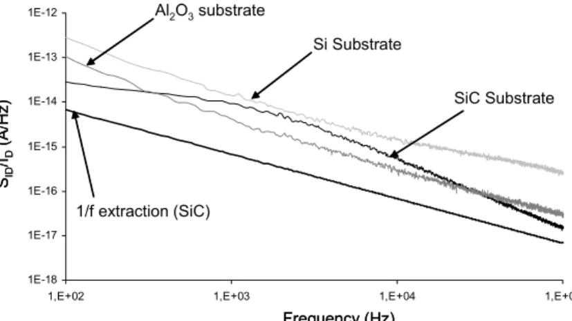
LFN Measurements - Saturated Biasing Operating Mode
Devices on sapphire and silicon with a single 1/f dependency exhibit a proportional
variation of SID versus ID. But the presence of the G-R centers for devices on SiC is
much more difficult to model. From figure 3, we can notice the trapping contribution (4 G-R centers) and the lower 1/f extracted source for devices on SiC. Some of these G-R centers can be attributed to trapping effects due to the presence of hydrogen in the 2DEG (that behaves as an acceptor in n-GaN, and traps the carriers [5]).
1E-18 1E-17 1E-16 1E-15 1E-14 1E-13 1E-12
1,E+02 1,E+03 1,E+04 1,E+05
Frequency (Hz) SID /ID (A /H z) 1/f extraction (SiC) SiC Substrate Al2O3substrate Si Substrate 1E-18 1E-17 1E-16 1E-15 1E-14 1E-13 1E-12
1,E+02 1,E+03 1,E+04 1,E+05
Frequency (Hz) SID /ID (A /H z) 1/f extraction (SiC) SiC Substrate Al2O3substrate Si Substrate
FIGURE 3. Normalized spectral density for a 0.15x2x50µm² HEMT (VGS=-2V, VDS=6V)
CONCLUSIONS
The results presented put forward the differences on the LFN performances of
AlGaN/GaN HEMT grown on Al2O3, Si, and SiC substrates. Devices on SiC exhibit
the best contact process and 2DEG layer quality, in spite of the presence of numerous G-R centers. This technology is still promising, once removing these defects.
ACKNOWLEDGMENTS
The authors would like to thank the French Ministry for Scientific Research and ESA for their financial support (contracts RNRT ANDRO and N°16013/02/NL/CK).
REFERENCES
1. M-A. di Forte-Poisson et Al., “MOCVD growth of group III nitrides for high power, high frequency applications” in Phys. Stat. Sol. (c) 2, No. 3, 2005, pp. 947-955.
2. F. Semond et Al., “Molecular Beam Epitaxy of group-III nitrides on silicon substrates : growth properties and device applications”, Phys. Stat. Sol. (a), No 2, 2001, 188, pp. 501-510
3. J.G. Tartarin et Al., “Using low frequency noise characterization of AlGaN/GaN HEMT as a tool for technology assessment and failure prediction”, Noise in Devices and Circuits II, Proc. of SPIE, Vol. 5470, Maspalomas, Spain, May 2004, pp.296-306.
4. J.M Peransin et Al., “1/f noise in MODFET’s at low drain bias”, IEEE Trans. On Electr. Dev., Vol. 37, No. 10, pp. 2250-2253, Oct. 1990.
5. J.M Arroyo et Al., “Effect of Deuterium diffusion on the electrical properties of AlGaN/GaN heterostructures”, MRS-symposium E March 2005, San Francisco, USA.