THESE
THESE
En vue de l'obtention du
DOCTORAT DE L’UNIVERSITÉ DE TOULOUSE
DOCTORAT DE L’UNIVERSITÉ DE TOULOUSE
Délivré par l'Université Toulouse III - Paul Sabatier Discipline ou spécialité : Génie Electrique
JURY G. AMARATUNGA/Rapporteur F. FAVIER/Rapporteur M. BRUNET/Directeur de Thèse P. SIMON/Directeur de Thèse K. GUERIN/Examinateur P.-L. Taberna/Invité D. Pech/Invité
Ecole doctorale : Génie Electrique, Electronique et Télécommunications (GEET) Unité de recherche : LAAS & Institut Carnot CIRIMAT
Directeur(s) de Thèse : M. BRUNET & P.SIMON Rapporteurs :
Présentée et soutenue par HUANG Peihua Le 8 Janvier, 2013
Titre : On-chip Micro-supercapacitors based on Nano-structured Carbon
Acknowledgement
First and foremost, I would like to thank my supervisors, Magali Brunet and Professor Patrice Simon. It has been an honor to be their PhD student. They have been good examples of researchers for me to follow. I am also grateful for all the ideas, time, and funding they offered both to establish and enrich my PhD experience. Their enthusiasm and passion for research are impressive and brought me through difficult periods during my PhD pursuit.
My PhD was much more difficult than I had imagined. There was always something not functioning or that could not be explained by commonsense. Fortunately, there were also Pierre-Louis Taberna and David Pech, who were always there to help me by analyzing experiments details and trying to find the key issues which stopped me from advancing in my research.
Our collaborator at Drexel University in Philadelphia (USA) Min Heon, prepared many CDC film samples for me and Professor Yury Gogotsi always participated in the discussion of the topic even with his extremely busy schedule. In addition, the warm reception I received during my stay at Drexel University was unforgettable. Members in the group were also source of friendship and allowed me to integrate quickly into the team and the community.
Working in the clean room, many of the operations were carried out by the technicians. I was thankful to them for my samples as soon as possible, sometimes even after hours. I would like to particularly mention Monique Benoit for her organization of affaires in the clean room; Pascal Dubreuil for his work in reactive ion etching; Laurent Bouscayrol for the use of the ovens; Pierre-Francois Calmon for his fabrication of masks; David Colin and Samuel Charlot for wire-bonding process; Franck Carcenac for the great training of SEM; Laurent Mazenq for
the training and help of photolithography process; and Ludovic Salvagnac and Sébastien Pinaud for the deposition of metal.
In both labs (LAAS and CIRIMAT) that I worked in, administrative staffs were indispensable. My thanks to Claude Laffore (ISGE LAAS), Marie Estruga (GEET), Camille Cazeneuve (Personnel LAAS) and Nicole Luga (CIRIMAT), whose efficient help meant that I could work without worrying about the administrative affaires.
I gratefully acknowledge the funding sources that made my PhD work possible, PRES for this 3-year contract and PUF for the two trips to Drexel University.
The time during my PhD was made enjoyable in large part thanks to the many friends that became a part of my life, Barbara, Emilie, Julie, Jérémy, Wanyu, Lorie, Etsuro and Rongying from the lab and Valerie, Chantal, Zhongda, Yijun, Hong and Tong, etc. Thank you for accompanying me and listening.
For this PhD thesis, I would like to thank the rapporteurs: Professor Gehan Amaratunga and Professor Frederic Favier, for their time, interest and helpful comments as well as another member of my defense committee, Katia Guerin, for her time and insightful questions.
Lastly, I would like to acknowledge the contribution of my family. They have been supportive of my work since my decision to come abroad. It has not been easy for them, especially since I had been with them in the same city for 23 years. During my Masters and my PhD studies, despite the physical distance of almost 10,000 km, our hearts became much closer than when I was physically there with them. And without their support, I could never have made it through this PhD. In the summer of 2010, the trip I took with my mother in Europe is probably the best memory of my life, and it was satisfying to be able to repay some of their support.
Unfortunately, my uncle Gao passed away because of lung cancer at the very end of my thesis writing. I was planning to go back China to visit him after finishing the thesis draft, as he was already very sick at that time. It was such a pity I could not be there in time. He had treated me like his own daughter since childhood and was always very proud of me no matter what I was doing. I hope he is still here to be able to hear my gratitude to him… Thank you.
Peihua HUANG Université Paul Sabatier January 2013
Abstract
The increasing number of functions in portable electronic devices requires more and more energy and power within a limited space. Li-ion thin film or so-called micro-batteries are the current solution for power supply. Drawbacks of these storage elements are poor power performance with limited life-span and temperature range. Carbon-based micro-supercapacitors, on the other hand, are able to deliver energy in short time, thus offering high power capability, to work at low temperature and they present an unlimited life-span. This thesis proposes several carbon-based micro-supercapacitors, to be integrated on a silicon substrate together with other electronics components or sensors. They are foreseen as a potential replacement or complement of Li-ion micro-batteries to enhance the total performance of the whole power source system. The thesis work is mainly focused on adapted materials and technologies for enabling micro-supercapacitors realization.
Two types of on-chip micro-supercapacitors with planar interdigitated electrodes configuration were developed: one prepared from Electrophoretic deposition (EPD) and its combination of different carbon materials and different types of electrolytes, the other from patterned titanium or silicon carbide derived carbon film (TiC-CDC or SiC-CDC) on Si chip with different microfabrication techniques. Onion like carbon-based micro-supercapacitor by EPD shows high power delivery (scan rate up to 100V/s) in organic electrolyte, and high temperature range (-50 °C – 80 °C) in a eutectic mixture of ionic liquids. Different techniques for patterning carbide films have been developed to fabricate a CDC based micro-supercapacitor: reactive ion etching (RIE) or focused ion beam (FIB). TiC-CDC film based micro-supercapacitors show promising preliminary results. The developed technologies pave the way to a full and effective integration of micro-size energy storage devices on-chip.
Keywords: MEMS, micro-supercapacitor, onion like carbon, electrophoretic deposition, carbide derived carbon, reactive ion etching.
Table of Contents
General Introduction ... 1
Reference ...5
Chapter I Bibliographic Summary ... 7
I Macroscopic Supercapacitors ...7
I.1 Theory of Electric Double Layer Capacitors (EDLCs) ...8
I.2 Carbon Materials for Supercapacitors ...14
I.3 Electrolytes ...21
I.4 Electrochemical Characterization ...24
II Micro-supercapacitors...32
II.1 Microfabrication Techniques...32
II.2 State-of-the-art of micro-supercapacitors ...34
III Conclusion ...47
IV Objectives ...48
Reference ...49
Chapter II On-chip Micro-supercapacitors by Electrophoretic Deposition (EPD) .. 59
I Introduction ...59
II Materials & Electrolyte ...59
III Experimental...60
III.1 Design of the active area ...60
III.2 Micro-fabrication ...62
III.3 EPD conditions...63
III.4 Electrochemical Characterization ...65
IV Results & Discussion ...66
IV.1 Preparation of the substrate ...67
IV.3 Activated Carbon – Influence of the thickness of the active film ...69
IV.4 AC based on-chip micro-supercapacitors in PC based electrolyte...75
IV.5 OLC based micro-supercapacitor in PC based electrolyte – Ultra-high Power Performance ...83
IV.6 Electrochemical Characterization of OLC in ILM under extreme temperatures ...90
V Conclusion & Perspectives ...102
Reference: ...104
Chapter III Micro-supercapacitors from Carbide Derived Carbon (CDC) Film ... 109
I Introduction ...109
II Materials and equipments...110
III Reactive Ion Etching (RIE) of CDC ...115
III.1 RIE of SiC-CDC...115
III.2 RIE of TiC-CDC ...118
IV RIE of Carbides ...128
IV.1 RIE of SiC ...131
IV.2 RIE of TiC ...137
V FIB of TiC-CDC ...144 V.1 Experimental...144 V.2 Electrochemical characterization...146 VI Discussion ...147 VII Conclusion...149 Reference ...150 Conclusion ... 153 Perspectives ... 156
General Introduction
Portable electronic devices (PEDs), such as laptop computers, smart phones, tablet computers, referring to any non-stationary electronic apparatus with singular or multiple capabilities, have been widely developed in the last decades. Faster processing is always one of the most important objectives to achieve for PEDs; it requires more electronic components to process and transmit data, thus demanding higher power. On the other hand, multifunction in PEDs, for instance cameras, motion detection, lights, calls for additional MEMS (Microelectromechanical systems) such as sensors or actuators resulting in even higher power demands. However, high power – i.e. high rate discharge – reduces batteries run time (the time PED will run before it must be recharged), which is the major power source in PEDs. In contrast, from point of view of customers, longer battery run time is desired. To solve this contradiction, supercapacitors can offer a complementary solution for power sources, thanks to their high discharge rates. Placed in parallel of a battery, a supercapacitor helps increasing the run time of the power source and helps extending the battery’s lifetime [1]. Better portability, featuring smaller volume of PED, is also required by customers. While the size of active circuits diminishes quickly according to Moore’s Law [2], while at the same time numerous microsystems are introduced, the remaining issue is the size of power sources [3]. Thus batteries and supercapacitors, which could be integrated on-chip in millimeter or even micrometer size, are strongly required.
In some particular cases such as wireless sensor networks, the sensing node which contains MEMS (accelerometer, temperature sensors…etc) coupled with RF emitter and transceiver and micro-controller are expected to function independently, i.e. to be autonomous in energy. These sensors network can be implemented in structures permanently (for structure health monitoring) or spread around in the environment [4]: batteries with their limited lifetime
should be thus avoided. A way to obtain energy autonomy is to power MEMS through energy harvesting and storage units on the same chip. Current energy harvesting systems collect energy from environment such as vibration (mechanical energy), thermal gradient, photovoltaics (solar thermal energy), etc [5]. However, energy from environment is not always available, posing the problem of intermittence. Energy storage is unavoidable in this context: a solution could be carbon-based supercapacitors, since they present longer lifespan thanks to electrochemically stable carbon electrode [6]. For implementing supercapacitors on these applications, miniaturization (small foot prints, low profiles) is required together with resistance to harsh environment. In this context, miniaturization of an energy storage element such as a supercapacitor is a real challenge, especially if it is intended to be on-chip.
On-chip energy storage micro-devices allows size reduction but other advantages are foreseen: monolithic integration indeed with collective fabrication of the energy storage micro-device along with the MEMS and/or the power management active circuit could bring benefits such as: reduction of losses thanks to optimized and short connections, lower manufacturing costs and enhanced reliability.
Following the major advances in harvesting micro-devices for wireless sensors networks, research on micro-scale energy storage and in particular supercapacitors, has increased significantly in the last ten years. The first published micro-supercapacitors in the early 2000s were based on pseudo-capacitive electrode material (RuO2) in a sandwich configuration [7].
Later-on (from 2006), carbon-based micro-supercapacitors started to appear [8]. This emerging interest can be explained by the fact that carbon is the most widely used electrode material for macroscopic supercapacitors, since it is more stable electrochemically than any other electrode materials for supercapacitors. Furthermore, combined with organic electrolytes, large voltage window and large temperature ranges could be obtained. Carbon-based on-chip micro-supercapacitors have not been well developed, since there are still
several unsettled issues concerning technology. Most reported carbon-based micro-supercapacitors were either fabricated by non-widely used microfabrication techniques or their performance could not match the performance with the same electrode material in macroscopic supercapacitors, or neither.
Therefore, in this thesis, there are two principal objectives: first, establishing routine processes with widely used micro-fabrication techniques to process carbon materials into on-chip micro-supercapacitors; second, improving performance including power and energy density to offer an enabling solution of energy storage on-chip.
The first chapter is a bibliographic summary. Macroscopic supercapacitors are firstly discussed. Principles and mechanisms of carbon-based supercapacitors are introduced with discussion of carbon electrodes materials and electrolytes, which are the most important components for carbon-based supercapacitors. Principles of electrochemical characterization including Electrochemical Impedance Spectroscopy (EIS) and Cyclic Voltammetry (CV) are explained to link the test results with performance. Micro-supercapacitors are then introduced with a description of common microfabrication techniques that are used to prepare the micro-devices. The state-of-the-art of micro-supercapacitors is discussed, especially carbon-based micro-supercapacitors, both in sandwich configuration and on-chip interdigitated configuration.
The second chapter describes all the carbon-based on-chip micro-supercapacitors prepared by electrophoretic deposition (EPD) technique. This collective deposition technique consists in processing carbon powder onto patterned current collectors. Pretreatment and EPD parameters were adjusted to achieve a homogeneous and adhesive carbon layer. Activated carbon (AC) was used in a three-electrode configuration to study the influence of thickness of the active film. Then the carbon was deposited on interdigitated current collectors to set up a routine processes. With AC, an improved power performance was found compared with
macroscopic AC-based supercapacitors in the same organic electrolyte. Onion-like carbon (OLC) was then used to further improve power density, although capacitance was compromised. Later, OLC-based on-chip micro-supercapacitors were tested in an ionic liquids mixture (ILM). Compared to organic electrolytes, an enlarged temperature range (-50 °C – 80 °C) was achieved with enlarged voltage window (3.7 V) and enhanced capacitance, hereby improved energy density.
The third chapter presents all the micro-supercapacitors fabricated from carbide-derived carbon (CDC) films which are binder-free films and proved to show large volumetric capacitance. Different processing strategies were developed to produce micro-supercapacitors: either by reactive ion etching (RIE) of CDC films, both SiC-CDC and TiC-CDC films or by reactive ion etching of carbide films (SiC or TiC) transformed later on into carbon films. Other than this, focused ion beam (FIB) was also used to fabricate micro-supercapacitors in micrometer range. Produced micro-micro-supercapacitors with interdigitated current collectors were tested electrochemically and their performance compared with macroscopic supercapacitors and with stat-of-the-art micro-supercapacitors.
Reference
1. Huggins, R.A., Supercapacitors and electrochemical pulse sources. Solid State Ionics, 2000. 134(1‚ 2): p. 179-195.
2. Moore, G.E., Lithography and the future of Moore's law. Proc. SPIE, 1995. 2437: p. 2-17.
3. Schmidt, M.A. Portable MEMS power sources. in Solid-State Circuits Conference,
2003. Digest of Technical Papers. ISSCC. 2003 IEEE International. 2003.
4. Srivastava, N., Challenges of Next-Generation Wireless Sensor Networks and its
impact on Society. Journal of Telecommunications, 2010. 1(1): p. 128-133.
5. Seah, W.K.G., E. Zhi Ang, and T. Hwee-Pink. Wireless sensor networks powered by
ambient energy harvesting (WSN-HEAP) - Survey and challenges. in Wireless
Communication, Vehicular Technology, Information Theory and Aerospace &
Electronic Systems Technology, 2009. Wireless VITAE 2009. 1st International
Conference on. 2009.
6. Pandolfo, A.G. and A.F. Hollenkamp, Carbon properties and their role in
supercapacitors. Journal of Power Sources, 2006. 157(1): p. 11-27.
7. Yoon, Y.S., et al., Solid-state thin-film supercapacitor with ruthenium oxide and solid
electrolyte thin films. Journal of Power Sources, 2001. 101(1): p. 126-129.
8. Ho, C., et al. Dispenser Printed Electrochemical Capacitors for Power Management
of Millimeter Scale Lithium Ion Polymer Microbatteries for Wireless Sensors. in
Chapter I Bibliographic Summary
I Macroscopic Supercapacitors
Although in different sizes, carbon-based micro-supercapacitors share the same charge storage mechanism, the same electrode materials and the same electrolytes with macroscopic supercapacitors.
While the first EDLC was described in 1957 [1], carbon-based supercapacitors have only been widely studied and developed since the 1990s [2].
Referring to the Ragone plot in Figure I.1 [3] which shows the specific power versus the specific energy of different energy storage devices, Li batteries, including Li primary batteries and Li-ion secondary batteries, show the best energy performance. Because batteries store energy in the bulk of electrode material via electrochemical reactions, the lighter the redox couple is, the higher the energy density is (per e- exchanged). However, concerning power density, because of the restriction from diffusion of electrolyte ions throughout the active materials (solid diffusion coefficient within the 10-10 to 10-14 cm2.s-1 range) as well as kinetics of electrochemical reactions, energy delivery can not be achieved in short times: power density is thus limited. Compared to batteries, electrochemical double layer capacitors have lower energy density but much higher power density, thanks to their mechanism of charge storage based on adsorption of ions on the surface of porous structured electrodes.
Figure I.1 Ragone Plot for various electrical energy storage devices [3].
I.1 Theory of Electric Double Layer Capacitors (EDLCs)
I.1.1 Conventional Capacitors
Conventional dielectric capacitors contain two parallel metallic plates with a dielectric material in between as shown in Figure I.2.
When there is a potential difference across the conductive plates, a static electric field develops across the dielectric layer, leading to charge accumulation on each plate. Energy is thus stored in the electrostatic field.
The quantity of charge stored is proportional to the potential applied according to Eq. 1. Eq. 1
!
Q=CV
where Q (A.s or Coulomb, C) is the charge stored in the capacitor. V (V) is the potential applied which is limited by the dielectric breakdown between the two plates and C (F) is the capacitance defined by Eq. 2.
Eq. 2 ! C A = "r"0 d
where A (m2) is the electrode surface area, d (m) is the distance between the layers of opposite charges, !0 is the dielectric constant of the vacuum (8.85!10-12 F.m-1) and !r is the relative dielectric constant of the materials introduced between the two plates. The dielectric materials adopted can neither be too thick or too thin. If it is too thick, the capacitance is largely reduced and more defects might be introduced. Then since a dielectric has a breakdown voltage MV/cm proportional to thickness, the minimum thickness is thus limited to ensure a certain operation voltage.
I.1.2 Supercapacitors
Electrochemical capacitors, also called Electrical Double Layer Capacitors (EDLCs) or Supercapacitors, are composed of two electrodes separated by an ionic conductive but electronic insulated separator soaked in an electrolyte (see Figure I.3).
Figure I.3 Representation of an EDLC with carbon as active materials (in the charged state) [4].
Charge storage is achieved through charge separation on a large surface area: the ions from the electrolyte are adsorbed onto a high specific surface area conducting active material. The extended high surface area is due to the porous structure of the active material, the carbon, which can reach up to 3000 m2/g, thus offering extremely high number of available sites to accommodate cations and anions in the electrolyte. The extremely thin layer (few nanometers or so in organic electrolytes) of charge separation corresponding to electrochemical double layer (EDL), compared with the “d” of Eq. 2, substantially enlarges the capacitance.
The EDL theory was firstly proposed by Helmholtz to describe the charge distribution at the interface of colloidal particles [5]. The EDL was then simply described as two layers of
opposite charge accumulated at the electrolyte/electrode interface (Figure I.4a). The separation between the layers of opposite charge was within the solvated radius of electrolyte ions, limited to the electrode surface. This model was later modified by Gouy and Chapman by introducing a diffuse model of the EDL, in which the potential at a surface decreases exponentially due to distribution of counter-ions from the electrolyte solution in the vicinity of electrode driven by thermal motion (Figure I.4b) [6, 7]. After, Stern combined the former two theories by dividing the area in the vicinity of the electrode into two parts, the compact layer right next to the electrolyte/electrode interface, also called Stern layer, and Diffuse layer [8] (Figure I.4c).
Figure I.4 Models of the electrochemical double layer at a positively charged surface: (a) the Helmholtz model, (b) the Gouy-Chapman model, and (c) the Stern model [9].
The Gouy-Chapman-Stern model shows that the interface behaves like the combination of the two capacitors in series:
Eq. 3 1 Cdl = 1 CHelmholtz + 1 CGouyChapman = d "r"0A + 1 "r"0#DA
where !D is the Debye length or 1/!D is diffusion length of Gouy-Chapman layer.
For highly concentrated electrolyte like in our case, 1/!D tends to 0 and then the double
layer capacitance can be defined as the Helmholtz capacitance: Eq. 4 ! 1 Cdl = 1 CHelmholtz
As defined by the modern EDL theory, an increase of the surface area (A) and a decrease of the ion and charged surface distance (d) in Eq. 2 respectively, both lead to the increase of capacitance. The energy stored in EDLCs is therefore several orders of magnitudes higher than conventional capacitors according to Ragone plot shown in Figure I.1 as the prefix “super-” indicates.
Since there is one double layer on each electrode of a supercapacitor, the total capacitance (cell capacitance) is thus written as:
Eq. 5
Hereby, the stored energy W (J) and the maximum power Pmax (W) are calculated according
to Eq. 6 and Eq. 7 respectively.
Eq. 6
Eq. 7
where R (!) is equivalent series resistance (ESR), the resistance of internal components of the supercapacitor such as current collectors, electrodes materials, electrolytes in supercapacitors. The voltage window is an important parameter in terms of both energy density and power density. However, the Pmax calculated here in Eq. 7 is the theoretical power
density that the device could reach according only to the voltage window and ESR; it is thus different from the useable power. Pmax is the power density where energy density close to 0 in the Ragone Plot. For real supercapacitor applications, there are several other factors that could take effect on the useable power density, like the thickness and porosity of electrodes, the voltage window, the series resistance, etc.
Since for supercapacitors the charge storage is achieved at the surface of the active materials, as opposed to batteries where electrochemical reactions occur in the bulk thus reducing the stability of electrodes, the cyclability of supercapacitors is much longer than batteries. In addition, this also leads to a better power performance for supercapacitors thanks to the absence of restriction of kinetics from electrochemical reactions.
To assess the efficiency of charging and discharging for EDL, the minimum time needed to reach a stable capacitance, named time constant, !(s), is introduced and defined by Eq.8 as follow.
Eq. 8
!
"=RC
Resistance of the capacitor, with its capacitance, defines time constant. High capacitance of supercapacitors, even with very low resistance, introduces several seconds of time constant.
Other than EDL capacitors, some other electrochemical devices have a “pseudo”-capacitive behavior but are based on kinetically fast faradaic reactions [10]. Typical materials are oxides (RuO2, MnO2, etc.) and electronically conducting polymers (polypyrrole, polyaniline, etc.).
Although the restriction from kinetics of reactions is alleviated, the limitations in power delivery and cyclability are still issues compared to EDL capacitors, whose electrode material is usually porous carbon.
I.2 Carbon Materials for Supercapacitors
Among all the carbon materials, activated carbons (ACs) are the most widely used active materials for EDLCs because of its high conductivity, high electrochemical stability, high surface area and relatively low cost. They can be obtained from various carbon rich organic precursors such as wood, pitch, coal, coke or fruit shell such as coconut or even synthetic polymer precursors [4]. The activation is carried out through either physical activation by high temperature treatment in oxidizing atmosphere or/and chemical activation by hot acidic or alkaline oxidation. Activation could be controlled by adjusting the reaction parameters, i.e. activation time, activation temperature etc... to create a porous network within the carbon grains leading to high specific surface area.
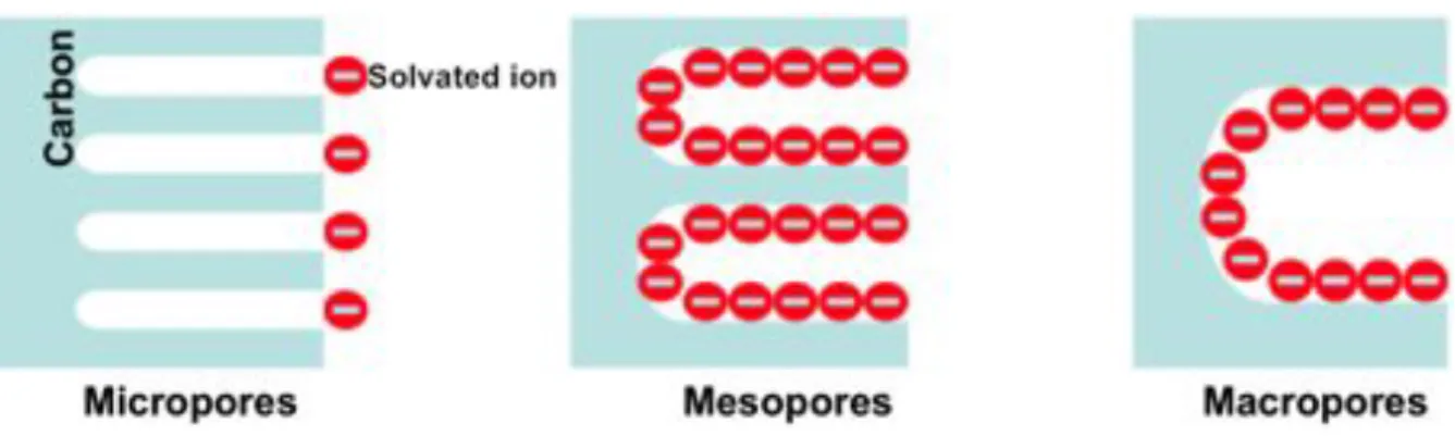
The activation treatments lead to the porous structure including all kinds of pores, as shown in Figure I.5, according to IUPAC [11], micropores with pore size smaller than 2 nm, mesopores with pore size between 2 nm and 50 nm, macropores with pore size larger than 50nm.
Figure I.5 Schematic diagram of the pore size network of an activated carbon grain.
The ratio between different types of pore size, i.e. the pore size distribution (for example Figure I.6), could be controlled by parameters of the activation process such as activation temperature and activation time or with different precursor. The specific surface area is
generally from 500 to 2500 m2/g, corresponding to the high specific capacitance around 100 – 150 F/g in organic electrolyte with operating voltage up to 3 V or in aqueous electrolyte around 200 F/g but only 1 V, since the electrolyte voltage window limits the cell voltage [3].
Figure I.6 Pore size distribution of an activated carbon YP-17 [12].
In spite of the high specific surface area of ACs, not all of the materials give high capacitance as expected [13, 14]. It was attributed to the inaccessibility of the solvated ions to the micropores as shown in Figure I.7 [15].
Figure I.7 Schematics of the traditional view of mechanism of the solvated ion adsorption in activated carbons (ACs).
Micropores (< 2 nm) were considered too small for ions to enter, since they are smaller than the size of the solvated ion, especially in organic electrolyte [15]. Consequently, they were thought to have no contribution to the charge storage, i.e., the capacitance. Macropores (> 50 nm) were too large to be fully occupied, thus wasting the pore spaces inside the active materials (dead volume), i.e., not efficient for maximizing the capacitance. Mesopores, as the compromise of the former two situations, were considered as the most ideal one to produce capacitance.
Therefore, plenty of efforts were made on adjusting most of the pores inside the carbon grain into the size around two times of the solvated ions sizes, i.e., (2 – 5 nm in organic electrolyte) which in the range of mesopores, to maximize the capacitance [16]. However, the improvement was not as distinct as expected. In contrary, several studies showed increased capacitance in mesoporous ACs with large amount of micropores [17-19]. The same phenomena were observed with microporous ACs [20]. A possible mechanism as the partial desolvation of the ions to enter into micropores was suggested [17-19, 21]. However, since the pore size cannot be finely controlled using activation treatments, ACs show a large pore size distribution, ranging between ~ 0.5 nm to ~ 5 nm. This large pore size distribution of ACs, involving still certain amount of mesopores and macropores even in microporous ACs, made the proposed mechanism quite suspicious. For example, a typical AC called YP17 shows a range of pore size around 1 nm, around microporous range (Figure I.6). However, there are still mesopores and macropores existing in YP17.
Finally, the effect of micropores was firstly observed using carbide derived carbons (CDCs) obtained through extraction of metals from carbides (TiC, SiC and other) by etching in halogens at high temperatures [22-24].
Eq. 9
!
TiC+2Cl2""HT#TiCl4+C
As shown in Eq. 9, the withdrawal of metals from crystalline structures of the carbides keeps the structures and leads to a controlled and narrow pore size distribution in CDCs. An anomalous increase in carbon capacitance was achieved with different temperature treated TiC-CDCs, i.e., with different sub-nanometer pore sizes ranging from 0.6 to 1.1 nm (Figure I.8) [24].
Figure I.8 (A) Plot of specific capacitance vs. average pore size and (B to D) schematic drawing of ions inside the pores with sizes (B) larger than 2 nm, (C) between 1 and 2 nm, (D) smaller than 1 nm [24].
The results were achieved in 1.5M NEt4BF4 acetonitrile (AN), in a 2-electrode
configuration, and the solvated ions diameter in this solvent are 1.3 and 1.2 nm respectively for cation and anion. The normalized capacitance decreases with the decrease of pore size and unexpectedly increased at around the solvated ion size. The gravimetric and volumetric capacitances obtained by CDCs are around 50% and 100% respectively higher than that of
ACs. Thanks to the very narrow pore size distribution, the increase of the normalized capacitance could be attributed to diminishing pore sizes, hence making the partial desolvation mechanism [24] proposed earlier for the microporous ACs, more consistent.
Carbide derived carbon structure was analyzed by Raman spectroscopy [25], which is a standard non-destructive analysis tool widely used for characterization of carbon materials. In Raman spectra recorded in the near-infrared and visible light regimes, carbon materials typically exhibit two broad bands, called D (disordered) and G (graphitic). The presence and position of D- and G-peaks, their intensity ratio (ID/IG) and full width at half maximum
(FWHM) can be used to extract the structural information of the materials. Appearance of both peaks in visible Raman spectra depends fundamentally on the ordering of sp2 sites and only indirectly on the fraction of sp3 sites. The G-peak appears due to the in-plane bond-stretching motion of pairs of C sp2 bonded atoms. This mode does not require the presence of six-fold benzene rings, it occurs at all sp2 sites. The D-peak is symmetry forbidden in perfect graphite and is activated only in the presence of disorder (sp3 structure). The spectra of CDC show two main features: the D- and G-peaks situated around 1350 cm-1 and 1600 cm-1, respectively (Figure I.9). The peak positions, their intensities (ID/IG) and full width at half
maximum (FWHM), as well as their wavelength dependent dispersion, were used to obtain information about the degree of disorder in CDCs.
Figure I.9 Raman spectra of TiC-CDCs made at different temperatures recorded using wavelengths indicated in the figure [25].
Chlorination at different temperatures leads to different carbon structures. Corresponding to the sharper peaks at higher temperature in Raman spectra, TiC-CDC is better organized at higher temperature with more graphitic structures in TEM pictures (Figure I.10), thus more conductive.
Figure I.10 TEM pictures of TiC-CDCs produced by chlorination of TiC at a) 400 °C, b) 800 °C, c) 1000 °C and d) 1200 °C with a scale bar at 5 nm [26].
Other carbon materials, especially carbon nanomaterials such as carbon nanotubes (CNTs) [27, 28] and onion like carbon (OLC) [29-31] can be used as active materials in EDLC electrodes. Despite a specific surface area much lower than activated carbons (1300 m2.g-1 for CNTs and 500 m2.g-1 for OLC), these exohedral carbons have a non-porous fully accessible surface area helps fast charging and discharging of supercapacitors and show high conductivities that facilitate the polarization of the device.
OLC is synthesized through annealing of nanodiamond powder at high temperatures [32] to graphitize the nanodiamond into OLC. A spherical particle of OLC is shown in Figure I.11. The bent graphitic layers in the onion were observed. Thanks to the highly graphitized structure, the conductivity of OLC is very high, similar to carbon black (around 4 S.cm-1) [33]. Specific surface area is around 500 m2.g-1, in a moderate range.
Figure I.11 TEM picture of an OLC particle.
Lack of porous structure obviously sacrifices the capacitance without enough surface area to accommodate electrolyte ions. However, these spherical particles allow ultrafast adsorption
and desorption of electrolyte ions, since there is no need to diffuse or even squeeze into pores. In spite of the high cost, high power supercapacitors have been prepared with OLC [29, 30].
I.3 Electrolytes
According to Eq. 6 (W=CV2/2) and Eq. 7 (Pmax=V2/4R), the voltage is a key factor for increasing both the energy and power performance of supercapacitors. The voltage window is usually limited by electrolyte. Being able to apply into all kinds of electrochemical devices, four types of electrolytes widely used in carbon-based symmetric supercapacitors are introduced here: aqueous electrolytes, organic electrolytes, gel polymer electrolytes and ionic liquids.
I.3.1 Aqueous Electrolytes
Aqueous electrolytes, i.e. water-based electrolyte, are widely used in electrochemical devices because of their high ionic conductivity (1 S.cm-1) and high capacitance when used in supercapacitors, but the water electrolysis beyond 1 V limits the operating voltage, as well as both the energy and power densities, and thus their applications. However, using aqueous electrolytes is more convenient for assembly of supercapacitors with no particular caution, while electrolytes with voltage window > 1 V are usually assembled in dry room with H2O
content lower than 1 ppm. Aqueous electrolytes are thus widely used in supercapacitors, since they are easier to handle. Acid and basic aqueous solutions such as H2SO4, H3PO4 or KOH are
the most widely used aqueous electrolytes thanks to their high conductivity.
I.3.2 Organic Electrolytes
Organic electrolytes show larger voltage window stability (up to about 5 V) instead of 1 V in aqueous electrolytes. As a result, supercapacitors using organic electrolytes show higher cell voltage. Although the conductivity of organic electrolytes is at least one order of
magnitude lower than aqueous ones, they are still preferred as the energy density is largely improved. The most widely used organic solvents are acetonitrile (AN) and propylene carbonate (PC). AN has a lower boiling point (bp 82 °C) and a higher melting point (mp -45 °C), compared to PC (bp 241 °C and mp -55 °C). Despite a low flash point (5 °C), AN still prevails over PC thanks to a lower viscosity that reduces the internal resistance of the devices.
Table I.1 Comparison of organic solvents acetonitrile vs propylene carbonate.
Solvent m.p. /°C b.p./°C Flash point/°C Viscosity (25 °C)/mPa.s Dielectric constant (20°C) Acetonitrile (AN) -48 81 - 82 5.5 0.369 36.64 Propylene carbonate (PC) -55 241.7 132 2.8 64.9
However, AN is starting to be substituted by PC, because it is flammable and harmful. Choice of salts for supercapacitor mainly depends on decomposing potentials of the solute ionic species. The preferred solutes are tetraalkylammonium salts of anions that are electrochemically stable, such as PF6-, BF4- and AsF6-. The most widely applied salt for
organic electrolyte is tetraethylammonium tetrafluoroborate (NEt4BF4). The concentration of
electrolyte is usually determined by final conductivity of electrolytes and the operating temperature range. If the carbon pore size of the electrode material could be adapted to the electrolyte ion size, the capacitance and the energy density would increase significantly.
I.3.3 Gel Polymer Electrolytes
The gel polymer electrolytes started drawing attention since their introduction by M. Armand into the battery field [34]. Since then, gel polymer electrolytes have been widely developed as the conductivity of electrolyte was ensured to be used in electrochemical systems. For instance, KOH-PEO (potassium hydroxide – polyethylene oxide) gel polymer electrolyte was used in carbon aerogel based supercapacitor [35]. Compared with KOH aqueous electrolyte, resistance was comparable, but capacitance was decreased in half.
There are several advantages with gel polymer electrolytes: no volatile organic solvent and lightweight of electrolyte films. Nowadays, besides supercapacitors [36, 37], it could be also applied in other electrochemical systems such as electrochromic windows [38, 39] and sensors [40, 41]. This is the first type of solid-state electrolyte that could be applied to build an all-solid-state power source.
The gel polymer electrolyte is a two-phase system composed of ionically conducting medium (liquid electrolyte) entrapped in host polymer matrix.
The polymer matrix, based on poly(propylene), poly(vinylidene difluoride), poly(tetrafluoroethylene), poly(ethylene oxide) (PEO), polyaniline (PANI), poly(methyl methacrylate) (PMMA), is regarded as the supporting structure of the solid-state electrolyte to offer mechanical strength, but it has no influence on electrochemical processes in the device.
However, gel polymer electrolyte suffers from poor mechanical strength. On-going researches has already suggested several solutions, such as composite gel polymer electrolytes and porous polymer electrolytes.
I.3.4 Ionic Liquid
The advantage of organic electrolytes over inorganic electrolytes is the high voltage window, leading to high energy density. To further enlarge the voltage window, ionic liquids (ILs), with voltage window up to 6 V, were studied as electrolyte for supercapacitors applications [42].
ILs are solvent-free electrolytes (molten salt like sodium chloride at 800 °C), that are liquid at low temperature. Such ILs are called Room Temperature Ionic Liquids (RTILs). Basically, in ILs, there are organic anions and cations with asymmetric size and aspect ratio, which greatly reduces lattice energy and thus lower the melting point. A second key feature is the low vapor pressure even at an elevated temperature, which reduces the risk of flammability.
Although higher voltage window unquestionably increases the energy of the devices, the high viscosity and low conductivity of ILs drastically reduce the power performance at temperature lower than room temperature. To settle this issue, operation temperature of supercapacitors using ILs is usually at temperature higher than room temperature.
Supercapacitors rarely operate at high temperature except when used near electronic components generating heat, but this is not controllable source of heat. There is thus the need to extend the temperature window of such devices so they can operate at lower temperatures, while at the same time keeping the high temperature range.
In the case of aerospace or aircraft industry, the temperatures requirements are even more drastic with operation below 0 °C down to -50 °C. Work has been done by Brandon et al to design electrolytes for operation down to -60 °C based on AN/NEt4BF4 mixture. However,
these mixtures were limited at 50 °C at high temperature [43]. In order to use supercapacitors at low temperature as well as high temperature, temperature tolerance should also be developed. Recently, a eutectic mixture of ionic liquids (ILM) N-methyl-N-propylpiperidinium bis(fluorosulfonyl)imide (PIP13FSI) and N-butyl-N-methylpyrrolidinium
bis(fluorosulfonyl)imide (PYR14FSI) with a temperature range from -50 to 100°C during
electrochemical characterization of supercapacitors based on carbon nanotubes (CNTs) and onion like carbon (OLC) [31] was reported. This electrolyte could be of great interest as well for micro-supercapacitors, enlarging the temperature operation range.
I.4 Electrochemical Characterization
In this thesis, two electrochemical characterization techniques were mainly used to measure the electrochemical performance of the micro-supercapacitors fabricated: Electrochemical Impedance Spectroscopy (EIS) and Cyclic voltammetry (CV).
I.4.1 Eletrochemical Impedance Spectroscopy (EIS)
Electrochemical impedance spectroscopy is a steady state technique used to distinguish individual contributions of various phenomena. A sinusoidal voltage punctuation of small amplitude (typically ± 5 mV) and frequency f (!=2"f) is superimposed to a bias voltage (stationary-state). Electrochemical impedance spectroscopy is obtained by scanning different frequencies, typically from 50 kHz to 10 mHz. The applied voltage is varied according to Eq. 10.
Eq. 10
!
V =V0+"V sin
( )
#twhere V0 is initial steady state potential of supercapacitor (V), in all study in this thesis, V0 is the open circuit potential of the cell, 0 V; #V is amplitude of the signal (V); ! the pulsation;
! = 2"f, where f is the signal frequency.
The response of this applied potential is a sinusoidal current, with amplitude of !I and a shifted angle " of phase indicated in Eq. 11.
Eq. 11
!
I t
( )
=I0+"I sin(
#t$%)
where I0 is the initial steady state current of the supercapacitor (A), in all study in this thesis, I0 is 0;
The potential applied and the current response could also be transformed to facilitate the mathematical treatment (Eq. 12 and Eq. 13):
Eq. 12
!
Eq. 13
!
I
( )
" =Imexp j[
(
"t # $)
]
The complex impedance is defined by the ratio between the applied voltage and current response (Eq. 14) Eq. 14 ! Z" =V
( )
" I( )
" = Vm Im exp( )
# j$The complex impedance is composed of a real part, corresponding to the resistance, and an imaginary part, corresponding to the capacitance.
The variation of impedance is usually represented in terms of Nyquist plot: the imaginary part of the impedance -Im(Z) is plotted versus the real part Re(Z) at different frequencies (Figure I.12c). The RC circuit models proposed in Figure I.14 fails to simulate Nyquist plot of real supercapacitors with three-dimensional porous electrodes. This porous electrode could be described as a succession of series/parallel RC components, according to De Levie model [44], with electrolyte ions reaching the outer surface area, which is in contact with the bulk electrolyte solution, then entering into the inner surface of the pore channels. This model (Figure I.12a) was proposed by De Levie in 1963 [45] with its equivalent circuit (Figure I.12b), called the Transmission Line Model.
Figure I.12 a) A schematic plot of Transmission Line Model proposed by De Levie and b) its equivalent circuit; c) an example of Nyquist plot of supercapacitors with activated carbon as electrodes in organic electrolyte [46].
The electrode shown in Figure I.12a has pores with cylindrical shape in uniform size. Upon potential polarization, electrolyte ions adsorption takes place at the outer surface of the electrodes. The transportation of electrolyte ions from bulk electrolyte onto the surface of the electrode causes a resistance corresponding to equivalent series resistance (ESR). Ions go deeper into the pore depth to charge C1, C2, C3,…Ci (as double layer capacitance along the
pore) with resistance R1, R2, R3,…Ri (as electrolyte resistance inside the pore). At high
frequency, the ions can only reach the outer surface of the electrolyte, with the real resistance as ESR. When frequency decreases, at mid-frequency, the ions can move deeper into the pores, thus showing higher resistance at lower frequency. At low frequency, both capacitance and resistance reach the maximum with no change theoretically, showing an almost vertical line. The cross point of the low frequency vertical line and the mid-frequency line is “the knee frequency”.
With Nyquist plot, the complex impedance could be written as Z = Re(Z) – jIm(Z). A supercapacitor could also be described as a combination of a resistor and a capacitor as
function of frequency f in series: the real part of impedance is the impedance of the resistor R and the imaginary part is the impedance of the ideal supercapacitor 1/(jC!). Hereby the complex impedance of this combined circuit could be also written in Eq. 15.
Eq. 15
!
Z =R(")+ 1
jC(")" = 1
jCcomplex" =Re(Z)# j Im(Z)
Complex capacitance Ccomplex could be represented as follow in Eq. 16 [46]. Eq. 16 ! Ccomplex = 1 "( j Re(Z)# Im(Z)) = j Re(Z)# Im(Z) "(Re2(Z)+Im2(Z))= j Re(Z)# Im(Z) 2$f (Re2(Z)+Im2(Z))
Thus, real part and imaginary part of the complex capacitance noted as C’ and C” respectively could be drawn out in Eq. 17.
Eq. 17 ! C'= "Im(Z) 2#f [Re(Z)2+ Im(Z)2] C"= Re(Z) 2#f [Re(Z)2+Im(Z)2]
where C’ is the capacitance of the supercapacitor; f is the frequency, Im(Z) is the imaginary part of the impedance and C” the loss.
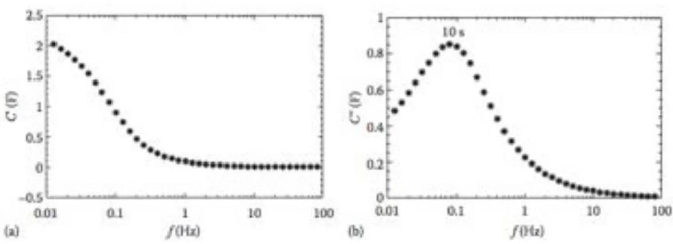
An example of real part and imaginary part of capacitance versus frequency is shown in Figure I.13.
Figure I.13 a) Real part and b) imaginary part of the complex capacitance versus frequency.
The capacitance of supercapacitors is defined by the plateau at low frequency (Figure I.13s). Specific capacitances of the devices have been normalized in this thesis by the footprint area of the device and the volume of a single electrode, respectively. With C” vs f (Figure I.13b), time constant ! could be extracted as the frequency fmax where C” reaches the maximum and ! =1/fmax. The smaller the time constant ! is, the faster the supercapacitor could be fully discharged with an energy efficiency ! 50 %, and the higher the real power delivery is.
I.4.2 Cyclic Voltammetry (CV)
Cyclic voltammetry has been used to investigate the capacitive behavior and the stability of supercapacitors with different active materials and different electrolytes within different voltage range.
A scan with potential changing linearly with the time at a constant rate is applied on the cell:
Eq. 18
where E0 is the initial potential of the scan, generally the rest potential of the cell (V), v is the scan rate (V/s), t is time (s).
To perform Cyclic Voltammetry experiment, the linear potential sweep is reversed when it reaches a set potential. The current response as a function of potential is recorded during the charge/discharge cycle.
Using the RC model proposed by De Levie [44], with an ideal supercapacitor of an identical capacitance at all voltage, when the scan rate dV/dt is constant, current
I=dQ/dt=CdV/dt is thus also constant. The cyclic voltammogram, as a perfect rectangular, is
shown in Figure I.14a. However, in reality, there are several factors can cause deviation from ideal CV plot. Equivalent Series Resistance (ESR) is introduced to be in series with the ideal capacitance and mainly defined by resistance of the electrolyte and electrode, leading to a period of time to reach a stable capacitive current, called time constant ! = RC. Before reaching the stable capacitive current, current slowly increases at the beginning of the positive scan and reverse scan, as shown in Figure I.14b. Another type of resistance is called leakage resistance, concerning undesired redox reaction or self-discharge inside the supercapacitor, thus in parallel to the capacitance. If the leakage resistance tends to ", it remains as an ideal supercapacitor. The smaller the leakage resistance is, the higher the leakage current is, as shown in Figure I.14c. The leakage resistance could be calculated from reciprocal of slope of the positive scan or negative scan. The combination of these two factors is shown in Figure I.14d, close to the real supercapacitor electrochemical signature. Despite this model, there are still several other factors affecting the shape of CV plots such as pore size distribution, especially for electrodes made of porous materials.
Figure I.14 Cyclic Voltammogram of a) an ideal supercapacitor, b) combination of a supercapacitor and a resistor in series or c) in parallel, d) a supercapacitor with resistors in series and in parallel at the same time.
From cyclic voltammetry technique, the capacitance of supercapacitor can be calculated from the integration of the current (by plotting current vs time using the potential scan rate) and dividing by voltage window, according to Eq. 1 Q=CV. The specific capacitance of the device will be then recalculated in terms of the footprint area of the micro-supercapacitors in this thesis.
II Micro-supercapacitors
Micro-supercapacitors, in this thesis, are defined as supercapacitors able to be integrated onto chip, where electrodes are not assembled with the help of clips or Swagelok cell but realized layer by layer. Micro-scale dimension is another characteristic of these devices. To operate at this scale, microfabrication is necessary to produce micro-supercapacitors.
Microfabrication includes the processes for fabrication of miniature structures, usually in micrometer size or even smaller in a collective way on or within a single substrate such as silicon. In the microelectronics industry, miniaturization of integrated circuits (IC), which are composed of silicon-based electronic components, is possible thanks to the permanent improvement of microfabrication technologies. The integration of new functions, i.e. sensors, actuators or other MEMS (Micro Electro Mechanical Systems), forced the industry to develop technologies allowing surface and bulk micromachining of silicon substrate.
Hereafter, we introduce microfabrication techniques for depositing materials in thin film form and patterning them. Then, state-of-the-art micro-supercapacitors will be overviewed with a particular focus on the different strategies adopted to integrate non-conventional active materials (such as carbon) in a planar configuration and achieve at the same time high performance.
II.1 Microfabrication Techniques
Devices prepared by microfabrication are generally not self-supported but formed on a support substrate with thickness in micro-scale. Silicon, largely used in microelectronics and MEMS is the most logical solution (available, well-known). The substrate offers an easy handling platform for the device during several steps of different fabrication processes. Except for semi-conductors components, the substrate is usually only for supporting purpose. Materials in thin-film form [47], i.e. conductors, insulators, or semiconductors (for
microelectronics) are then deposited on the substrate to create the microdevices. For optical applications, deposited thin films could be reflective, transparent, light guiding or scattering. Films could also have chemical or mechanical properties according to the application. Deposition techniques could be divided into two categories: growth and deposition. Growth includes thermal oxidation for very thin oxide layers and epitaxy [48]. Deposition includes chemical vapor deposition and physical vapor deposition which comprises sputtering and evaporation, electrodeposition and printing techniques [49]. It will be shown later in this chapter that the most commonly used deposition techniques in micro-supercapacitors are sputtering and electrodeposition for pseudo-capacitive materials (RuO2) [50] and printing
techniques for carbon powders [51, 52].
The deposited layers in most cases should be patterned in order to realize different functions. The patterning is generally from millimeter scale to nanometer scale, which is the feature of micro-fabrication. The most widely applied patterning technique is photolithography: the use of a chromic mask to transfer the desired pattern onto the thin-film followed by etching [53]. Etching is the process of removing unwanted part from a thin film in order to form the pattern in micrometer scale. The part of unprotected film is exposed to etchant that can physically or chemically attack the target materials until they are totally removed. Etching techniques include dry etching and wet etching. Dry etching, or plasma etching, includes ion beam etching and Reactive Ion Etching (RIE) [54]. In RIE, the thin film is attacked by ionized chemically active plasma where high speed is generated by an electric field. Thus, both chemical etching and physical etching are involved in RIE. The etch rate and selectivity of chemical etching and physical could be adjusted by source power and bias power, respectively, according to the properties of thin film etched and the protecting layer. Wet etching involves usually chemical agent to dissolve part of the unprotected thin film.
Another possible technique, to pattern a thin film, is to grow it through a mask: for instance electrodeposition through a photoresist mask. Alternatively, a physical mask (called shadow mask or stencil) can be placed directly on the substrate during deposition. The deposition technique can be sputtering or evaporation or even screen-printing.
Direct writing [55] such as inkjet printing [52] could be applied automatically to the substrate to transfer the material by contact, offering other possibilities for patterning. The material is deposited only on the necessary areas, thanks to a head. Alternatively nanoimprint where a stamp (made of nano or micro features) inked with the desired material, can be used.
Focus ion beam (FIB) can also be used to physically etch away undesired part to pattern with heavy ions without any protection as the ion beam is focused.
To fabricate on-chip micro-supercapacitors that are able not only to be integrated into Microsystems, but also be of good performance, fabrication techniques should be chosen carefully.
II.2 State-of-the-art of micro-supercapacitors
Micro-supercapacitors were firstly reported in 2001 [50]. Since then, there have been several models developed. However, it is early stage of technology and many microfabrication techniques combined with the synthesis of active materials are under test.
Electrode materials of micro-supercapacitors evolve from easy fabricated but expensive ruthenium oxide [50, 56-58] to widely used carbon materials with advanced microfabrication techniques [52, 59-62].
There have been already several trials on fabricating thin-film electrodes with different materials deposited with different techniques such as RuO2-SnO2 electrode via reactive
sputtering [58], carbon nanotubes/graphenes via layer by layer (LBL) [63], cone-shaped polypyrrole/RuO2 via anodic deposition [64] and carbide derived carbon film via chlorination
[59, 65], etc. Thin films of carbon nanotubes and chemically reduced graphenes were synthesized by layer-by-layer assembling [63]. A volumetric capacitance of 160 F.cm-3 for the 350 nm thick hybrid carbon layer was achieved in 0.5 M H2SO4 aqueous electrolytes,
higher than its macroscopic supercapacitors in the same electrolyte (130 F.cm3), thanks to the thin layer of electrode.
Although not ready for integrating on-chip, these electrodes could be potentially used to fabricate on-chip micro-supercapacitors in the future.
In ready-to-integrate micro-supercapacitors, there are two configurations reported: stack configuration and interdigitated configuration shown in Figure I.15.
Figure I.15 Schematic pictures of a) a stack micro-supercapacitor and b) an interdigitated micro-supercapacitor.
Stack configuration forms a sandwich-like stacking with electrodes face to face and electrolyte in between. A separation between the electrodes is necessary: it can either be an insulating layer soaked with the electrolyte or the solid electrolyte itself. It is similar to macroscopic supercapacitors, but the different layers (electrodes and electrolyte) are
deposited by microfabrication techniques one after another to form the stack. The layers are then patterned and contacts are created to achieve the final integrated micro-device. Interdigitated configuration generally involves microfabrication on a substrate (in most cases silicon, but it can also be a polymer) with electrodes patterned in interdigitated form. The separation in this case is the lateral spacing between the interdigitated fingers.
For the purpose of making a summary, in this section, we divide reported supercapacitors into two categories: stack supercapacitors and interdigitated micro-supercapacitors. They have small footprint area (~ or < 1 cm2) and small thickness (< 100 µm) and easy to be integrated into Microsystems. In addition, as microfabrication is involved during the process of realizing micro-supercapacitors, at the early stage of development, groups specialized in microfabrication took lead showing proofs of concepts with electrochemical data sometimes incomplete. Moreover, as different groups have different way of calculating the capacitance and/or energy density, it is difficult to compare directly by reported figures. Thus, in order to compare performance, capacitance, energy density and power density were recalculated according to the footprint area of the micro-scale device in this section.
II.2.1 Stack micro-supercapacitors
II.2.1.1 On a substrate
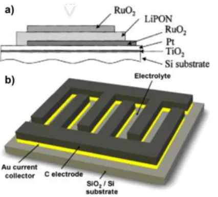
Most of the early works done as micro-supercapacitors were using metal oxides as active materials thanks to the large variety of deposition techniques (sputtering, atomic layer deposition – ALD, electrodeposition) available, despite poor conductivities (~ 10-6 S.cm-1). A stack RuO2-based micro-supercapacitor with Li2.94PO2.37N0.75 (LiPON) as electrolyte was
firstly reported in 2001 by simple sputtering deposition [50]. This system was selected because thin film of LiPON electrolyte had been successfully applied for thin film batteries
[66]. Despite LiPON was used instead of conventionally used proton H+ for RuO2 electrode, a
capacitance of 47.5 mF.cm-2 was obtained within 2.5 V.
Later on, the same research group published on LiPON-based stack micro-supercapacitor modified by co-sputtering of RuO2 with tungsten (W) to enlarge the interspace of atoms in
RuO2 to facilitate the mobility of Li+ [57]. The modified stack micro-supercapacitor achieved
200 mF.cm-2 per footprint area capacitance under 2.5 V.
Electronically Conducting Polymers (ECPs), another electrode material for pseudo supercapacitors, have also been studied for stack micro-supercapacitors. Example of a polymer-based stack micro-supercapacitor was composed of polypyrrole (PPy)-decorated nanoporous gold (NPG) as electrode material and an aqueous HClO4-poly(vinyl alcohol)
(PVA) gel as electrolyte. 1.8 mF.cm-2 and 0.65 mJ.cm-2 were achieved as specific capacitance and specific energy, respectively, within 0.85 V [67].
One of the first carbon-based stack micro-supercapacitor was reported in 2006 [68] with 99 wt% Super P carbon black (with specific surface area of 62 m2.g-1) and 1 wt% polyvinylidene fluoride binder in N-Methyl-2-pyrrolidone as electrode material using not widely used microfabrication technique: Origami fabrication as shown in Figure I.16.
Figure I.16 A schematic illustration of carbon-based stack micro-supercapacitor fabricated via origami (left) and its electrochemical performance (right) in 1.5 M H2SO4 [68].
The device was electrochemically characterized in 1.5 M H2SO4 aqueous solution. Only 0.6
V was reached and poor capacitive behavior was presented by cyclic voltammogram at a scan rate of 50 mV/s. Specific capacitance of 0.8 mF.cm-2 per footprint area and specific energy of 0.2 mJ.cm-2 was achieved in this micro-supercapacitor.
During the same year, another stack micro-supercapacitor fabricated by dispenser printing of electrodes of mesocarbon microbead (with specific surface area of 10 m2.g-1) in a PVDF polymer binder and BMIM+BF4- ionic liquid in PVDF gel electrolyte was realized [51]. Poor
capacitive behavior with a severely distorted CV plot was presented within 2 V voltage window. Electrochemical performance of this micro-supercapacitor was measured with specific capacitance of 0.3 mF.cm-2 per footprint area and specific energy density of 0.5 mJ.cm-2.
These two examples were only proof of concept of carbon-based stack micro-supercapacitors. The low specific surface area materials (62 m2.g-1 for the Origami fabricated device and 10 m2.g-1 for dispenser printed device) also explain the low capacitance.
Moving from low specific surface area carbon to carbon nanotubes (CNTs) as active material, higher energy and power densities could be obtained for flexible printable stack micro-supercapacitors [69]. An ideal capacitive behavior marked by quasi-rectangular shape of CV plot (at 10 mV/s within 3 V) was presented in organic electrolyte (1 M LiPF6 in 1:1
ethylene carbonate/diethylcarbonate by weight). A specific capacitance of 1.2 mF.cm-2 per footprint area could be achieved in aqueous-based gel eletrolyte PVA/H3PO4. The capacitance
was not high, because single-walled carbon nanotubes (SWCNTs) thin-films (0.6 µm) were sprayed onto the current collector surface. Despite the low capacitance, at least better capacitive behavior was achieved (Figure I.17).
Figure I.17 Cyclic voltammetry of SWCNT supercapacitor in (a) PVA/H3PO4 polymer electrolyte and (b)
LiPF6/EC:DEC. Galvanostatic charge/discharge curves measured with a 1 mA/cm2 (30 mA/mg) current density for a
thin film SWCNT supercapacitor using (c) PVA/ H3PO4 polymer electrolyte and (d) LiPF6/EC:DEC. [69]
II.2.1.2 Flexible stack micro-supercapacitors
As opposed to thin films deposited on a hard substrate (silicon), there are cases of micro-supercapacitors with stack configuration where the substrate is flexible (paper, polymer) or where one of the electrodes itself is flexible. A possible application field is the emerging printable electronics. For those flexible devices, several techniques can be applied to build the stack. Examples found in literature are mainly based on carbon nanotubes, such as Meyer rod coating method of CNT ink [70], layer-by-layer (LBL) assembling [63, 71], laser writing of graphenes [72] and CVD of CNTs [73]. Flexible micro-supercapacitors were fabricated from CVD of CNTs. The CNTs were vertically aligned on the current collectors as shown in Figure I.18 along with nanoporous cellulose paper soaked with various electrolytes. High specific
capacitance of 330 mF.cm-2 was achieved with 50 µm thick CNTs layer in ionic liquid electrolyte [73].
Figure I.18 Schematic pictures of the flexible micro-supercapacitors with electrochemical characterization results. [73]
Stack micro-supercapacitors, despite the large footprint areas, present still one dimension in micrometer scale. Theoretically, micro-scale device should be able to offer better performance than macroscopic supercapacitors regarding the size effect. The thinner the electrode layer is, the better the electrolyte ions could reach the full carbon layer. With this idea, several ultra-thin carbon-based supercapacitors were realized with the thickness less than 10 nm. In this scale, there should be no problem of adhesion between electrode materials, as there is little amount of powder to load on the electrodes.
A stack micro-supercapacitor was fabricated with only 10 nm of pristine graphene and multilayer reduced graphene oxide by “in-plane” fabrication approach as shown in Figure I.19 [74].
![Figure I.3 Representation of an EDLC with carbon as active materials (in the charged state) [4]](https://thumb-eu.123doks.com/thumbv2/123doknet/2219485.14702/20.892.123.805.100.669/figure-representation-edlc-carbon-active-materials-charged-state.webp)
![Figure I.16 A schematic illustration of carbon-based stack micro-supercapacitor fabricated via origami (left) and its electrochemical performance (right) in 1.5 M H 2 SO 4 [68]](https://thumb-eu.123doks.com/thumbv2/123doknet/2219485.14702/47.892.130.774.804.1031/figure-schematic-illustration-supercapacitor-fabricated-origami-electrochemical-performance.webp)
![Figure I.20 Schematic illustration of on-chip micro-supercapacitors based on CNTs and its electrochemical performance in BMIM + BF 4 - ionic liquid [82]](https://thumb-eu.123doks.com/thumbv2/123doknet/2219485.14702/52.892.127.766.593.846/figure-schematic-illustration-micro-supercapacitors-electrochemical-performance-liquid.webp)