HAL Id: hal-02552636
https://hal.archives-ouvertes.fr/hal-02552636
Submitted on 4 Jan 2021HAL is a multi-disciplinary open access archive for the deposit and dissemination of sci-entific research documents, whether they are pub-lished or not. The documents may come from teaching and research institutions in France or abroad, or from public or private research centers.
L’archive ouverte pluridisciplinaire HAL, est destinée au dépôt et à la diffusion de documents scientifiques de niveau recherche, publiés ou non, émanant des établissements d’enseignement et de recherche français ou étrangers, des laboratoires publics ou privés.
ALD of ZnO:Ti: Growth Mechanism and Application as
an Efficient Transparent Conductive Oxide in Silicon
Nanowire Solar Cells
Damien Coutancier, Shan-Ting Zhang, Simone Bernardini, Olivier Fournier,
Tiphaine Mathieu-Pennober, Frédérique Donsanti, Maria Tchernycheva,
Martin Foldyna, Nathanaelle Schneider
To cite this version:
Damien Coutancier, Shan-Ting Zhang, Simone Bernardini, Olivier Fournier, Tiphaine Mathieu-Pennober, et al.. ALD of ZnO:Ti: Growth Mechanism and Application as an Efficient Transparent Conductive Oxide in Silicon Nanowire Solar Cells. ACS Applied Materials & Interfaces, Washington, D.C. : American Chemical Society, 2020, 12, pp.21036 - 21044. �10.1021/acsami.9b22973�. �hal-02552636�
ALD of ZnO:Ti : growth mechanism and application
as efficient transparent conductive oxide in silicon
nanowire solar cells
Damien Coutancier,1,2 Shan-Ting Zhang,1,2 Simone Bernardini,1,3 Olivier Fournier,1,4 Tiphaine
Mathieu-Pennober,5 Frédérique Donsanti,1,4 Maria Tchernycheva,5 Martin Foldyna,6 Nathanaelle
Schneider*,1,2
1 Institut Photovoltaïque d’Ile-de-France (IPVF), 18 boulevard Thomas Gobert, 91120 Palaiseau,
France
2 CNRS, UMR 9006, Institut Photovoltaïque d’Ile-de-France (IPVF), 18 boulevard Thomas
Gobert, 91120 Palaiseau, France
3 TOTAL, 18 boulevard Thomas Gobert, 91120 Palaiseau, France
4 EDF R&D, IPVF, 18 boulevard Thomas Gobert, 91120 Palaiseau, France
5 Centre de Nanosciences et de Nanotechnologies, UMR 9001 CNRS, Univ. Paris-Saclay, 10
Boulevard Thomas Gobert, 91120 Palaiseau Cedex, France.
KEYWORDS Atomic Layer Deposition, TCO, ZnO:Ti, n-type, QCM studies, silicon nanowire
solar cells
ABSTRACT
In the quest for replacement of indium-tin-oxide (ITO), Ti-doped zinc oxide (TZO) films have
been synthesized by atomic layer deposition (ALD) and applied as n-type transparent conductive
oxide (TCO). TZO thin films were obtained from titanium (IV) i-propoxide (TTIP), diethyl zinc
and water, by introducing TiO2 growth cycle in a ZnO matrix. Process parameters such as the order
of precursor introduction, the cycle ratio and the film thickness were optimized. The as-deposited
films were analyzed for their surface morphology, elemental stoichiometry, optoelectronic
properties and crystallinity, using a variety of characterization techniques. The growth mechanism
was investigated for the first time by in situ quartz-crystal microbalance measurements. It
evidenced different insertion modes of titanium depending on the precursor introduction, as well
as the etching of Zn-Et surface groups by TTIP. Resistivity as low as 1.2 × 10⁻³ Ω cm and
transmittance > 80% in the visible range were obtained for 72-nm thick films. Finally, the first
application of ALD-TZO as TCO was reported. TZO films were successfully implemented as top
electrodes in silicon nanowire solar cells. The unique properties of TZO combined with conformal
coverage realized by ALD technique make it possible for the cell to show almost flat EQE
1. INTRODUCTION
Wide band gap oxides have gained great interest as transparent electrode materials in a large range
of optoelectronic devices. The most widespread transparent conductive oxide (TCO) is
indium-tin-oxide (ITO) due to its superior optoelectronic properties (resistivity ρ = 10-4 Ω cm,
transparencies > 90%).1 However, the scarcity of indium and thus the ever-rising price of ITO has
urged researchers to develop alternative materials. Zinc oxide (ZnO) is a low-cost wide bandgap
(3.30 eV) semiconductor composed of nontoxic and abundant raw materials that can be doped by
various elements (Al, B, F, Ga, I, Mg,…), which makes it a promising TCO.2 Furthermore, it is
equally essential to develop suitable deposition techniques to grow TCO in order to fulfil specific
requirements of devices. For example, in terms of nanostructured systems, it is often critical to
enable a conformal deposition of TCO materials with a fine control of the film properties
(thickness, work function, doping level, etc.) to generate efficient systems.
In particular, the silicon nanowire (Si NW) solar cells prepared using plasma-assisted
vapor-liquid-solid (VLS) growth have been recently introduced in the form of monolithically integrated
modules on a single glass substrate.3 The module is formed by series connection of multiple cells
required for industrial upscaling and it was the first time that the active area of Si NW based radial
junction solar module reached 10 cm2. While the large series resistance of first modules has been
reduced by depositing a thick ITO top contact followed by a printed dense Ag grid on top,4 issues
are still to be addressed stemming from the non-conformal ITO deposition and the large shadowing
issues caused by the grid. The shadowing induced loss of collected current from areas covered by
non-transparent Ag contact, which directly transfers into conversion efficiency loss. A
desirable to achieve reduced series resistance and increased transparency, which leads to increased
solar cell performance.
Atomic layer deposition (ALD) is well suited for the preparation of n-type wide band gap
semiconductors, and has been implemented in various optoelectronic architectures.5,6 By
sequentially repeating self-saturated surface reactions, ALD allows growth of uniform and
conformal materials with controlled properties under relatively soft conditions.7,8 Extensive
studies on preparing TCOs by ALD have been reported, which highlights the unique capabilities
of ALD.5,6 Contrary to materials deposited using conventional methods, ALD-TCOs usually
consist of a host matrix with rather dispersed atomic dopants. Such particular arrangement is made
possible thanks to the reaction-surface growth mechanism characteristic of the ALD technique and
the use of various doping strategies.5,6 Both undoped and doped zinc oxide have been extensively
investigated by ALD.9,10 Typically, diethylzinc (DEZ) and deionized water (H2O) are used as
precursors for Zn and O atom sources. Doped materials are usually obtained by inserting a dopant
growth cycle in between an integer number of ZnO cycles, leading to what is referred to as an
ALD “supercycle”. For instance, for ZnO:Al (AZO), the most commonly investigated doped-ZnO
material by ALD, {Al2O3} dopant cycle are inserted in ZnO growth. The Al-doping level can be
varied by tuning the cycle ratio of {Al2O3} with respect to {ZnO}. Other parameters reported to
affect the doping include the order of precursor introduction,11–13 the deposition temperature,14 and
the pulse or purge duration times.15–17 The doping level can also be modified by co-injecting the
Zn and Al precursors,18 by using alternative Al precursors19,20 or inhibitors.21,22 Despite the several
advantages of ALD-AZO in terms of synthesis (e.g., relative ease of access to {Al2O3} process)
AlOx phase segregation, and some challenges remain to improve its electrical properties as
efficient TCO electrode.
Titanium is another promising dopant atom for ZnO. Compared to Al, Ti has higher valency, thus
could potentially provide more charges per atom. The lower growth rate of TiO2 (growth per cycle,
GPC ~ 0.36 Å/cycle) relative to Al2O3 (GPC ~ 1.3 Å/cycle) can facilitate a better distribution of
dopant atoms and thus reduce the formation of undesired TiOx nanoprecipates.23 Moreover,
titanium-doped zinc oxide (TZO) has a higher work function than AZO which for example makes
it more suitable as anode for OLED applications.24 Compared to AZO, TZO by ALD has been
explored to a much smaller extent,23,25–29 and so is the Ti-Zn-O system.30–33 Most processes for
TZO use DEZ, H2O and titanium (IV) i-propoxide (TTIP) as precursors, with a supercycle
strategy.23,25–27,29 The influence of the cycle ratio on the material properties has been previously
investigated for different film thicknesses and the optimum range of cycle ratio is reported
{TiO2}:{ZnO} ~ 1:10 – 1:20.25–27,29 Resistivity values as low as 8.9 × 10⁻⁴ Ω cm with high
transparencies (>80%) have been obtained for 100 nm-thick films.23 Kim et al. compared AZO
and TZO thin films by ALD and they highlighted the advantages of using Ti rather than Al as
dopant, namely lower concentration of inactive dopant, higher electron mobility and higher doping
efficiency.23 The doping mechanism of TZO has been further investigated by Torrisi et al.28
However, except for the effects of the supercycle ratio and the deposition temperature, none of the
other reported ALD doping modification methods have been tested on TZO. Also, very little is
known on the surface chemistry and growth mechanism of TZO by ALD. Finally, despite its
promising properties, to the best of the authors’ knowledge, ALD-TZO has never been applied as
The aim of this work is to gain a deeper understanding of the growth mechanism of ALD-TZO as
well as to prove its feasibility as TCO in optoelectronic devices, and in particular in Si NW based
solar cells by reporting the first application of ALD-TZO thin films as TCO. A thorough
investigation of the material growth mechanism by in situ quartz crystal microbalance (QCM) was
first carried out to understand the surface chemistry involved and ensure the fine control of the
Ti-doping in zinc oxide. Subsequently, by tuning the process parameters (i.e. sequence of precursor
introduction, cycle ratio, thickness), TZO films with optimized opto-electrical properties were
obtained, in line with ones reported in the literature. Finally, the ALD-TZO thin films were applied
as transparent electrode materials in Si NW solar cells and were demonstrated not only to work
efficiently as TCO material, but also to lead to a superior external quantum efficiency (EQE)
response in comparison to ITO.
2. EXPERIMENTAL SECTION 2.1. Material Synthesis
TZO thin films were prepared in a BENEQ TFS-200 ALD reactor. Diethylzinc (Zn(C2H5)2, DEZ,
EpiPure, SAFC), titanium (IV) i-propoxide (Ti(OiPr)4, TTIP, min. 98%, STREM) and deionized
water were used as Zn, Ti, and O sources, respectively. All chemicals were used without further
purification. Nitrogen (N2, 99.9999%, Air Liquide) was used as both carrier and purging gas. TTIP
was heated in a hot solid source system Beneq HS300 at TTTIP = 85 °C while other precursors were
kept at room temperature. Experiments were performed at Tdep = 200 °C and the pressure in the
reaction chamber was kept in the range of 1 - 2 mbar. Thin films were deposited simultaneously
on borosilicate glass, single- and double-polished n-doped Si (100) wafer with native oxide top
and i-propanol (5 min each), while Si (100) substrates were cleaned in a detergent solution (RBS
35 Concentrate, 2 % in water, 5 min) and rinsed with deionized water.
TZO film depositions were performed with the following program: [TZO] = n . (n1 . {ZnO} +
{TiO2}) where n and n1 are the number of supercycles and the ratio of ZnO and TiO2 cycles
{ZnO}:{TiO2}, respectively. The former was varied in a range of values from 22 to 445 whereas
for the latter values of 1, 2, 5, 10, 20 were selected. The zinc oxide growth cycle, i.e. {ZnO}, was
performed according to reported procedure.13 Two precursor sequences were investigated and
referred to as sequence A (H2O pulse / N2 purge / DEZ pulse / N2 purge) where the first pulse is a
H2O pulse; and sequence B (DEZ pulse / N2 purge / H2O pulse / N2 purge), where the first pulse
is a DEZ pulse. A titanium oxide growth cycle, i.e. {TiO2}, corresponds to {TiO2} =
{[TTIP]/N2/H2O/N2 = [0.5/0.05/0.5/0.5]/5/2/5 s} and “combination” mode was chosen to ensure
proper mass transport of TTIP. “Combination” mode is composed of four steps ([t1/t2/t3/t4]). First,
N2 is injected in the TTIP source (t1), then all valves are kept closed (t2), TTIP precursor is pulsed
(t3). Finally, N2 is injected with simultaneous precursor pulse (t4).
2.2. In-situ Quartz Crystal Microbalance (QCM) measurements
In-situ QCM measurements were acquired with a Colnatec Eon-LT monitor system, using a HT
quartz crystal covered by an aluminum alloy (6 MHz initial oscillation frequency) located on the
cover lid of the reactor. Signal was recorded every 0.1 s and the lowest thickness step precision
was 0.04 Å (for pure ZnO films, the conversion was made with impedance acoustic value Zf =
0.556 and ZnO density of 5.61 g/cm3 as input parameters). Measurements were done after a
stabilization time of 1 hour in order to reach a uniform and constant temperature in the whole
and ensure an effective saturation state, longer pulse and purge times were chosen. An average
over at least five TZO supercycles was performed in order to improve the measurement precision.
2.3. Material Characterization
TZO thin film characterization was performed on samples deposited on silicon wafer
(ellipsometry, GIXRD, XRR) or borosilicate glass (Raman, Hall effect measurement,
spectrophotometry). Thin film thicknesses were determined by spectroscopic ellipsometry (SE)
performed with a Horiba Jobin Yvon Uvisel 2 ellipsometer, and X-ray reflectivity (XRR) using a
PANalytical Empyrean equipment using Cu-Kα radiations. For the former, SE measurements in
the wavelength range of 200-1700 nm were modelled using a Tauc-Lorentz oscillator function.
X-ray diffraction (XRD) studies were performed under grazing incidence (GIXRD) conditions for
crystallinity determination and phase detection. Thin film compositions and morphologies were
obtained using a Merlin VP Compact scanning electron microscope (SEM) provided by Zeiss
equipped with an energy dispersive X-Ray spectroscopy (EDS) detector from Bruker.
Transmittance and reflectance spectra were obtained using an Agilent Cary 500 UV-Vis-NIR
spectrophotometer equipped with an Agilent Diffuse Reflectance accessory. Electrical
measurements were performed on samples with an area of 2.25 cm2 at room temperature using
four-point probe measurement setup (LucasLab Probe 4 apparatus) and an ECOPIA HMS-5000
system with a 0.556T permanent magnet was used for Hall effect measurement. Values of
resistivity, carrier concentration, and electron mobility are the average of at least three
measurements. Raman spectra were recorded using a Horiba Labram HR spectrometer in the
micro-Raman mode (backscattering geometry) at room temperature. A UV laser (λ=325nm) was
2.4. Solar cell device preparation and characterization
The radial junction solar cells based on silicon nanowires were fabricated on commercial
soda-lime glass substrate (2.5 x 2.5 cm2) coated by FTO. The p-type doped Si NWs were grown by
plasma-assisted vapor-liquid-solid (VLS) process in plasma-enhanced chemical vapor deposition
reactor at substrate temperature of 420 °C. Nanowire arrays were subsequently coated by p-type
doped aSi:H followed by an intrinsic aSi:H absorber layer, with the p-i-n junction finished by a
thin n-type aSi:H film. The details of the process can be found elsewhere.3 The front TCO contact
used was either the conventional ITO (240 nm) deposited by sputtering or ZnO:Ti grown by ALD.
The J–V characteristics of the solar cells were measured under standard AM1.5G (100 mW/cm2)
illumination conditions (Newport solar simulator) calibrated using a certified crystalline silicon
solar cell. A circular mask with diameter of 4 mm was used during the measurement to control the
illuminated area. The external quantum efficiency (EQE) was measured on an Oriel IQE 200 setup
at room temperature.
3. RESULTS AND DISCUSSION
3.1. In situ QCM measurements of TZO during ALD growth
To optimize the TZO film properties, it is critical to realize a fine tuning of the Ti-doping by
controlling the surface chemistry involved during the growth. Mass variations relying on molecule
desorption and adsorption during the film deposition have been evidenced by recording in situ
QCM measurements.
Figure 1a and Figure 1b display the mass variations of one growth cycle in pure ZnO and TiO2 films. In case of ZnO thin films, positive mass variations are recorded after both H2O (Δm1ZnO)
and DEZ (Δm2ZnO) pulses. As described earlier by Elam et al., this is attributed to the successive
surface reactions:
n (OH)* + DEZ n O-ZnEt* + n C2H6
during the DEZ pulse, and
n O-ZnEt* + H2O n O-ZnOH* + n C2H6
during the H2O pulse, where * represent the surface species and n the number of hydroxyl groups
reacting during each {ZnO} cycle.34 The n value can be determined from the (Δm1ZnO / Δm2ZnO)
ratio. In our case (Δm1ZnO / Δm2ZnO) = 0.05, which corresponds to n = 1.54. This is in accordance
with reported values (n = 1.37 as determined by QCM, n = 1.56 as determined by quadrupole mass
spectrometry).34,35 In case of TiO2 thin films, mass variation is positive after TTIP pulse (Δm2TiO2)
and negative after H2O pulse (Δm1TiO2). This finding has been attributed to the following surface
reactions by Aarik et al.:
n (OH)n* + Ti(OiPr)4 O-Ti(OiPr)4-n* + n iPrOH
during the TTIP pulse, and
O-Ti(OiPr)4-n* + H2O n O-TiOH* + (4-n) iPrOH
during the H2O pulse, where * represent the surface species and n the number of ligand released
during the TTIP pulse.36,37 The n value can be determined from the (Δm1TiO2 / Δm2TiO2) ratio, and
here (Δm1TiO2 / Δm2TiO2) = -0.67. It corresponds to n = 3.3, which is slightly higher than reported
value (n = 2.2 – 2.5 at Tdep = 200-250 °C).36
The mass variations that occur during the doping cycle {TiO2} in ZnO, as in TZO films, were
recorded. The order of precursor introduction is well-known to impact the surface reactions and
thus the film properties.11–13 Hence, two sequences were investigated for ZnO: the TTIP pulse
recorded mass evolutions for both sequences are similar to the case where {TiO2} grows on itself
(Figure 1b). A positive mass variation is observed after the TTIP pulse (Δm2TiO2_A, Δm2TiO2_B)
while a negative one is seen after the H2O pulse (Δm1TiO2_A, Δm1TiO2_B). However, the ratio
(Δm1TiO2_A/B / Δm2TiO2_A/B) have values (Δm1TiO2_A / Δm2TiO2_A = -0.35 and Δm1TiO2_B / Δm2TiO2_B
= -0.37) that correspond to different n values than when TiO2 grows on itself (n = 2.7 for sequence
A, n = 2.6 for sequence B and n = 3.3 for pure TiO2). These findings demonstrate that the TiO2
growth is affected by the substrate, as is characteristic of ALD growth. It also shows that the
growth of TiO2 is rather hindered upon depositing on the ZnO surface, as suggested by other
groups.23,25,26,31 The mass uptakes during the TTIP pulse alone and over the complete {TiO2} cycle
are both larger in sequence B than in sequence A (Δm2TiO2_A = 0.82 a.u. vs Δm2TiO2_B = 1.69 a.u.;
Δm1TiO2_A + Δm2TiO2_A = 0.53 a.u. vs Δm1TiO2_B + Δm2TiO2_B = 1.06 a.u.). This can be explained by
the relative higher reactivity of TTIP towards OH surface species (as in sequence B) than
Zn-Et ones (as in sequence A). The mass variation observed in sequence A when TTIP is pulsed on
Zn-Et terminated surface can be due to TTIP reacting either with Zn-Et surface groups, remaining
–OH surface groups, or both. To discriminate these three possibilities, a specific film deposition
sequence was designed: 10 × {TiO2} / H2O pulse / N2 purge / DEZ pulse / N2 purge / 10 × {TiO2},
and the mass variations during the last ten {TiO2} cycles were recorded and compared (Figure
1e). For all ten cycles, the mass variation is positive during the TTIP pulse. However, the mass
gain is negative after the first {TiO2} cycle, but positive and constant for the following nine cycles.
The negative mass gain after the first cycle shows that TTIP reacts and replaces the Zn-Et surface
fragments (Ti being lighter than Zn). This etching mechanism can be attributed to the higher bond
energy of Ti-O vs Zn-O (ETi-O = 666.5 kJ.mol-1 vs EZn-O = 159.4 kJ.mol-1).38 Similar etching can be
after the first cycle (Figure 1e) as compared to a positive mass gain in sequence A (Figure 1c)
most likely originates from the difference of the surface and the top layers. , When the top layers
are TiO2-based (Figure 1e) rather than Znbased (TZO from sequence A, Figure 1c), the
O-ZnEt bond is weaker hence more reactive and more Zn-Et fragments can be etched by TTIP. In
addition to this, the number of remaining hydroxyl groups can be expected to be different, notably
due to the surface poisoning effect of iPrOH.39 Additional experimental work such as residual gas
analysis could provide direct evidence of the etching mechanism. A similar behavior has been
reported for ALD-AZO thin films.11,13,19,20,40 In summary, different Ti insertion mechanisms
following two different precursor sequences are clearly evidenced from the QCM studies, which
Figure 1. Mass variations recorded by in situ QCM measurements during the growth of (a) pure
ZnO films; (b) pure TiO2 films; (c) {TiO2} doping cycle in ZnO (sequence A); (d) {TiO2} doping cycle in ZnO (sequence B); (e) 10 × {TiO2} on a substrate composed of 10 × {TiO2} / H2O pulse/ N2 purge / DEZ pulse / N2 purge.
3.2. Influence of the process parameters on ALD TZO thin film properties
3.2.1. Influence of the sequence of precursor introduction
The order of precursor introduction can have a strong impact not only on the film growth
mechanism, but also on its final properties by for example improving the distribution of dopant
atoms and reducing the formation of nanolaminate structures, as previously demonstrated for
Al-doped ZnO thin films.11–13 Thus, TZO films have been synthesized with two different sequences
for the {ZnO} cycle, namely sequence A (H2O pulse / N2 purge / DEZ pulse / N2 purge) and
sequence B (DEZ pulse / N2 purge / H2O pulse / N2 purge), with constant cycle ratio (n1 = 10 i.e.
{TiO2}:{ZnO} = 1:10) and supercycle number (n = 44). The main properties of the obtained films
are compared in Table 1, Figure 2, Figure 3 and in Supporting Information (Figure S1).
TZO films grown by both sequences show similar morphology and structural properties. In
particular, they are both polycrystalline and adopt the ZnO würtzite structure. The crystallites have
an apparent rice grain shape (average grain size ~ 80 nm), which is different from the round shaped
grains of undoped ZnO (Figure 2), as described elsewhere.27 The sequence B leads to thicker films
with higher [Ti]/[Zn] atomic ratio (as determined from EDS measurements), which is consistent
with its higher mass gain observed previously by QCM analysis. In fact, in case of sequence B,
the TTIP precursor is pulsed on an OH-terminated surface, which is more reactive than a Zn-Et
terminated and/or remaining –OH surface fragments. In case of sequence B, the measured
[Ti]/[Zn] atomic ratio equals to 3.1 at% (Table 1), above the solubility limit of Ti in ZnO (2 at%).41
This indicates the potential presence of amorphous TiO2 phase at grain boundaries as observed by
others via transmission electron microscopy.29 Even though sequence B (with higher Ti content)
leads to films with a higher carrier concentration (N = 5.5×10²⁰ vs 2.5×1020 cm-3), it seems that a
certain portion of Ti atoms does not act as active dopant but rather as scattering centers, which
gives rise to a lower film mobility (µ = 6 vs 20 cm2 V-1 s-1). As a consequence, the overall film
resistance is higher for sequence B than for sequence A. In Raman measurement of undoped ZnO,
with the resonance UV excitation one identifies the sharp first-order A1(LO) vibrational modes of
würtzite ZnO located at 575 cm-1.42 The broad band on the lower wavenumber region is likely an
overlap of several Raman bands such as E2high (438 cm-1, first order), 2LA (485 cm-1, second order)
and so on.42 It has been reported that when ZnO is doped with Al, an additional contribution at
around 510 cm-1 appears and the intensity of this defect-related peak is correlated to the
conductivity of ZnO:Al thin films: the more conductive the AZO film, the higher the intensity of
the defect-related peak.43,44 The same trend is observed here for ZnO:Ti films as shown in Figure
3a where indeed an additional contribution at 518 cm-1 is clearly visible. The peak intensity is
lower for the TZO film of sequence B, which is consistent with its sheet resistance being higher
than that of sequence A. Similarly to ZnO:Al, a red shift of A1(LO) peak is also observed in Ti
doped ZnO. Both films are equally transparent with transmittance values above 80% in the
400-1300 nm region (Figure 3b), which is in agreement with previously reported ALD-TZO films.23,25–
28 Finally, as the target properties for a TCO are high transmission and conductivity values, the
Table 1. Main properties of TZO films obtained from sequences A and B with n = 44 and n1 = 10.
Sequence Thickness (nm) Carrier conc. (cm-3) (cmMobility 2 V-1 s-1) (Ω/sq) R
[Ti]/[Zn] (at%)EDS
A 73 2.5 × 10²⁰ 20 160 0.9
B 82 5.5 × 10²⁰ 6 295 3.1
Figure 2. Top SEM images of (a) ZnO, (b) TZO of sequence A and (c) TZO of sequence B. The
scale bar is 100nm. The film thickness of all three samples are similar, around 80 nm.
Figure 3. (a) Raman spectra of undoped ZnO, TZO of sequence A and B. The sheet resistance is
indicated for TZO of both sequences while undoped ZnO is so resistive that its sheet resistance value is not shown. (b) Optical transmittance (solid lines) and reflectance (dotted lines) for the
3.2.2. Influence of the cycle ratio {TiO2}:{ZnO} and the film thickness
By varying the cycle ratio n1 {TiO2}:{ZnO} and the number of supercycle n in ALD, the Ti-doping
and thickness of TZO film can be varied, which in turn affects the opto-electrical properties of the
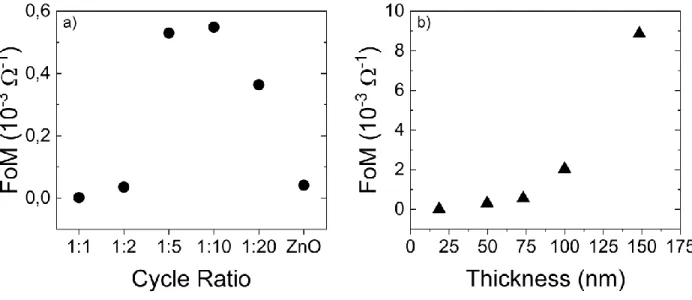
resulting TZO films. For TCO materials, the classical Haacke’s figure of merit (FoM) is often used
to evaluate the overall performance. FoM is defined as:45
FoM=T 10 R
where T is the transmittance at 550 nm and R the sheet resistance. TCOs used in solar cells
usually exhibit transmittance of 80% and sheet resistance of 10 Ω/, which yields FoM (in unit
of 10-3 Ω-1) of around 10.
In order to avoid possible formation of TiO2 nanolaminates,7 the number of {TiO2} cycle was kept
at 1 while the number of {ZnO} cycles (n1) is varied from 1 (high Ti-doping) to 20 (low Ti-doping). As shown in the Supporting Information (Figure S2 – Figure S6), the film thicknesses are lower
than the values expected from the linear combination of GPCTiO2 (0.35 Å/cycle) and GPCZnO (1.68
Å/cycle), suggesting that a different growth mechanism is taking place for TZO when compared
to pure ZnO and TiO2. Furthermore, the GPC of TZO films decreases with increasing Ti
incorporation, which highlights a substrate-dependent growth behavior, typical of ALD deposition
technique. These findings are in accordance with results previously reported25,26 and with our
QCM observations. The obtained films have density values in the range of 5.3 – 5.8 g.cm-3, which
is similar to the ZnO density.9,10 As shown in the Supporting Information (Figure S3), TZO films
adopt either a polycrystalline ZnO würtzite structure (n1 ≥ 2) or a ZnTiO3 nanocrystalline one (n1
300-1200 nm region) with optical gap values between 3.2 and 3.7 eV, which is in agreement to
previously reported results.26 The refractive index n at 633 nm decreases from 2.00 for pure ZnO
to 1.86 for TZO with 1:5 cycle ratio. At higher Ti concentration, the apparent increase of n could
indicate the formation of nanoprecipitates of TiO2.26 Finally, all films are n-doped with carrier
concentration in the order of 1020 cm-3, probably caused by substitutional Ti and potential H doping
from the precursor.26,46 As is seen in Figure 4a, the TZO film prepared with cycle ratio
{TiO2}:{ZnO}=1:10 shows the highest FoM, suggesting that TZO film prepared at this ratio gives
the best compromise between optical and electrical properties.
As a consequence, the ratio {TiO2}:{ZnO}=1:10 was kept the same, while the supercycle numbers
were varied from 22 to 82 to grow TZO films of different thicknesses. This resulted in films with
a thickness in the range 9 – 148 nm. A linear growth was observed, with an average GPC value of 1.46 Å/cycle, and almost no nucleation delay was observed (Figure 5). As shown in Supporting
Information (Figure S7 - Figure S9), films of all thicknesses are fairly transparent in the visible
range, and the optical properties are independent of the film thickness. All films are n-doped and
the carrier concentration slightly increases with the film thickness (N = 1020-1021 cm-3), as well as
the mobility (1 – 150 cm2 V-1 s-1), which is in accordance to previously reported systems.23,25–
27,29 It seems that thinner films (thickness < 50 nm) suffer significantly from the grain boundaries
scattering due to the presence of smaller grains.27 The resistivity of all films is in the order of 10-3
Ω cm; the lowest resistivity value of 5 × 10⁻⁴ Ω cm is seen for 150 nm thick films, which is slightly
more conductive than systems reported by Bergum et al.27
Interestingly, the FoM increases monotonically as a function of the film thickness for TZO (Figure
4b). In particular, for the 150 nm thick TZO film, FoM is fairly close to 10, suggesting that
Figure 4. Haacke’s figure of merit (FoM, in unit of 10-3 Ω-1) of TZO films as a function of (a)
cycle ratio and (b) film thickness (n1 = 10) during ALD deposition.
Figure 5. Influence of the supercycle number n on the TZO film thickness, as determined by
3.3. Application of ALD-TZO thin films as TCO in Si NW solar cells
As a reference, sputtered ITO with a nominal thickness of 240 nm was used as the front TCO in
the radial junction Si NWs based solar cells to provide sufficiently low resistance for smaller cell
areas with reduced total reflectance.47 However, as sputtering utilizes energetic particles, it often
results in a directional deposition: ITO deposited on top of the Si NWs is always found thicker
than that on the side walls of nanowires (see Figure S10 in Supporting Information). The lack of
conformal ITO front contact leads to an inhomogeneous charge collection and increased sheet
resistance of the device and thus prevents reaching the maximum final device performance. This
drawback can partly be compensated by increasing the ITO thickness which however leads to
optical losses.
Therefore, we demonstrate the ALD-TZO thin films for transparent contacts on a proof-of-concept
device which can improve the front contact transparency. Silicon NW solar cells with thin
amorphous Si absorber and a nanostructured surface morphology, which is particularly
challenging for contacting, were chosen for this demonstration. The TCO was deposited on top of
solar cells with the following structure: sodalime glass / FTO / p-type c-Si NW / p-type aSi:H /
aSi:H absorber layer / n-type aSi:H. The schematic drawing of the structure is shown in Figure
6a.47 The corresponding J-V characteristics are shown in Figure 6b. Devices show reasonable
series resistance, which validates the ALD-TZO layer as a proper contact film. Despite the
efficiency of 2.5 % being relatively low, a photovoltaic diode behavior is clearly seen, suggesting
that TZO film by ALD effectively works as a TCO in the nanowire solar cells.
As can be seen in Figure 6d, the external quantum efficiency (EQE) for a cell with sputtered ITO
EQE values are reduced in the wavelength range between 400 and 550 nm, similarly to previously
reported devices.47 Overall, the EQE response of the ITO-based device exhibits bell-like shape,
which is far from ideal. This is caused by the parasitic absorption in the thick ITO contact film. In
contrast, the cell coated with an 80 nm TZO by ALD shows an EQE curve of almost ideal
rectangular shape with some losses below the wavelength of 400 nm, thanks to the conformal
coverage of TZO over Si NWs as suggested in Figure 6c. In addition, the EQE values are greatly
improved to about 80 % over almost the whole visible range. This implies a significant reduction
of the parasitic absorptions (due to thick ITO layers) leading to a flat response between 400 and
650 nm wavelengths, which has been achieved for the first time for VLS-grown Si NW devices.
In comparison, the previously best achieved spectral response with sputtered ITO showing larger
parasitic losses in the wavelength range below 550 nm than in this work can be found elsewhere.48.
The record high EQE values with a very flat response have been achieved for the first time on
studied silicon nanowire solar cells. The SiNW devices represent a real challenge for the front
transparent contact materials as most of the deposition techniques fail to provide sufficient
conformality over the radial junction structure. Our ALD deposited TCO not only covers properly
the nanostructured surface, but it also provides superior opto-electrical properties (as shown by
EQE) when compared to any previously published results on radial junction devices on a glass
substrate. We have demonstrated that using TZO contact layer deposited by ALD technique can
significantly improve performance of any flat or (nano-)structured solar cell suffering from the
Figure 6. (a) Architecture of radial junction Si NWs solar cells. (b) J-V characteristics of the radial
junction Si NW solar cell covered by 80 nm ZnO:Ti by ALD as front TCO contact. The EQE of the same cell (solid line) is shown in (d) as compared to the EQE curve (dash dot line) measured on a cell with 240 nm ITO (by sputtering). (c) cross sectional SEM image of the radial NW structure showing conformal coverage by the top ZnO:Ti electrode (by ALD).
4. CONCLUSIONS
Transparent electrode materials are an essential component in most optoelectronic devices.
However, nowadays it still remains challenging to develop alternative materials to replace the
well-established ITO films using deposition techniques that are well adapted to devices with
complex structures. In this context, we report on the growth of titanium-doped zinc oxide (TZO)
by atomic layer deposition (ALD), and we demonstrate the successful implementation of TZO as
top electrode in silicon nanowire based solar cells.
In this work, TZO films were obtained from diethyl zinc, titanium i-propoxide and water as
precursors. Titanium-doping was achieved with a supercycle strategy. We investigated in great
details the surface reaction mechanisms during the growth of TZO via in situ quartz crystal
microbalance measurements. We verified that the order of the precursors introduction affects the
doping mechanism and consequently the final TZO film properties. In particular,
sequence-dependent surface chemistries, and the capacity of TTIP to replace –ZnEt terminated surface
fragments were demonstrated. Additional parameters such as the cycle ratio and the film thickness
were also optimized for TZO films grown by ALD, demonstrating their capacity to tune the TZO
properties. Finally, the ALD-TZO thin films were successfully applied as transparent electrode
materials in Si NW solar cells. The unique properties of TZO, as well as the conformal deposition
ensured by ALD resulted in an almost rectangular shape of the EQE curve of the Si NW device as
opposed to the unsatisfactory bell-shaped EQE curve obtained on devices employing an ITO
electrode.
In conclusion, ALD-TZO shows great potentials as an efficient top electrode in nanostructured
been proven. These findings open the way to many other possible applications of TZO as
ITO-alternative for optoelectronic devices.
ASSOCIATED CONTENTS Supporting Information.
The Supporting Information is available free of charge. It includes extra characterizations of TZO
films, i.e. the influence of the precursor sequence on the structural properties, the influence of the
cycle ratio on the film thickness, structural and opto-electrical properties, the influence of the film
thickness on the TZO structural properties. It also contains a cross sectional SEM image of the
radial NW structure with ITO top electrode.
AUTHOR INFORMATION
Corresponding Author
*E-mail: n.schneider@cnrs.fr (N. Schneider)
Funding Sources
This work was supported by the French Government in the frame of the program of investment
for the future (Programme d’Investissement d’Avenir ANR-IEED-002-01), the French Agence
Nationale de la Recherche under the contract numbers INDEED ANR-15-CE05-0019 and
HANAMI ANR-17-CE09-0022, and the EU ERC project “NanoHarvest” (grant no. 639052).
REFERENCES
(2) Transparent Conductive Zinc Oxide: Basics and Applications in Thin Film Solar Cells;
Ellmer, K., Klein, A., Rech, B., Eds.; Springer Series in Materials Science; Springer-Verlag: Berlin Heidelberg, 2008. https://doi.org/10.1007/978-3-540-73612-7.
(3) Al-Ghzaiwat, M.; Foldyna, M.; Fuyuki, T.; Chen, W.; Johnson, E. V.; Meot, J.; Roca i Cabarrocas, P. Large Area Radial Junction Silicon Nanowire Solar Mini-Modules. Sci Rep 2018,
8 (1), 1651. https://doi.org/10.1038/s41598-018-20126-5.
(4) Al‐Ghzaiwat, M.; Foti, A.; Nuesslein, A.; Halagacka, L.; Meot, J.; Labouret, A.; Ossikovski, R.; Cabarrocas, P. R. i; Foldyna, M. Toward Efficient Radial Junction Silicon Nanowire-Based Solar Mini-Modules. physica status solidi (RRL) – Rapid Research Letters 2019,
13 (2), 1800402. https://doi.org/10.1002/pssr.201800402.
(5) Leskelä, M.; Mattinen, M.; Ritala, M. Review Article: Atomic Layer Deposition of Optoelectronic Materials. Journal of Vacuum Science & Technology B 2019, 37 (3), 030801. https://doi.org/10.1116/1.5083692.
(6) Sheng, J.; Lee, J.-H.; Choi, W.-H.; Hong, T.; Kim, M.; Park, J.-S. Review Article: Atomic Layer Deposition for Oxide Semiconductor Thin Film Transistors: Advances in Research and Development. Journal of Vacuum Science & Technology A 2018, 36 (6), 060801. https://doi.org/10.1116/1.5047237.
(7) George, S. M. Atomic Layer Deposition: An Overview. Chemical Reviews 2010, 110 (1), 111–131. https://doi.org/10.1021/cr900056b.
(8) Miikkulainen, V.; Nilsen, O.; Li, H.; King, S. W.; Laitinen, M.; Sajavaara, T.; Fjellvåg, H. Atomic Layer Deposited Lithium Aluminum Oxide: (In)Dependency of Film Properties from Pulsing Sequence. Journal of Vacuum Science & Technology A 2015, 33 (1), 01A101. https://doi.org/10.1116/1.4890006.
(9) Gao, Z.; Banerjee, P. Review Article: Atomic Layer Deposition of Doped ZnO Films.
Journal of Vacuum Science & Technology A 2019, 37 (5), 050802. https://doi.org/10.1116/1.5112777.
(10) Tynell, T.; Karppinen, M. Atomic Layer Deposition of ZnO: A Review. Semiconductor
Science and Technology 2014, 29 (4), 043001. https://doi.org/10.1088/0268-1242/29/4/043001.
(11) Na, J.-S.; Peng, Q.; Scarel, G.; Parsons, G. N. Role of Gas Doping Sequence in Surface Reactions and Dopant Incorporation during Atomic Layer Deposition of Al-Doped ZnO. Chem.
Mater. 2009, 21 (23), 5585–5593. https://doi.org/10.1021/cm901404p.
(12) Pollock, E. B.; Lad, R. J. Influence of Dosing Sequence and Film Thickness on Structure and Resistivity of Al-ZnO Films Grown by Atomic Layer Deposition. Journal of Vacuum Science
& Technology A 2014, 32 (4), 041516. https://doi.org/10.1116/1.4885063.
(13) Le Tulzo, H.; Schneider, N.; Lincot, D.; Patriarche, G.; Donsanti, F. Impact of the Sequence of Precursor Introduction on the Growth and Properties of Atomic Layer Deposited Al-Doped ZnO Films. Journal of Vacuum Science & Technology A 2018, 36 (4), 041502. https://doi.org/10.1116/1.5030990.
(14) Ahn, C. H.; Lee, S. Y.; Cho, H. K. Influence of Growth Temperature on the Electrical and Structural Characteristics of Conductive Al-Doped ZnO Thin Films Grown by Atomic Layer Deposition. Thin Solid Films 2013, 545, 106–110. https://doi.org/10.1016/j.tsf.2013.07.045. (15) Lee, D.-J.; Kwon, J.-Y.; Kim, S.-H.; Kim, H.-M.; Kim, K.-B. Effect of Al Distribution on Carrier Generation of Atomic Layer Deposited Al-Doped ZnO Films. J. Electrochem. Soc. 2011,
158 (5), D277–D281. https://doi.org/10.1149/1.3568881.
(16) Genevée, P.; Donsanti, F.; Renou, G.; Lincot, D. Study of the Aluminum Doping of Zinc Oxide Films Prepared by Atomic Layer Deposition at Low Temperature. Applied Surface Science
2013, 264, 464–469. https://doi.org/10.1016/j.apsusc.2012.10.045.
(17) Park, H. K.; Yang, B. S.; Park, S.; Kim, M. S.; Shin, J. C.; Heo, J. Purge-Time-Dependent Growth of ZnO Thin Films by Atomic Layer Deposition. Journal of Alloys and Compounds 2014,
605, 124–130. https://doi.org/10.1016/j.jallcom.2014.03.169.
(18) Yuan, H.; Luo, B.; Yu, D.; Cheng, A.; Campbell, S. A.; Gladfelter, W. L. Atomic Layer Deposition of Al-Doped ZnO Films Using Ozone as the Oxygen Source: A Comparison of Two Methods to Deliver Aluminum. Journal of Vacuum Science & Technology A 2011, 30 (1), 01A138. https://doi.org/10.1116/1.3666030.
(19) Wu, Y.; Potts, S. E.; Hermkens, P. M.; Knoops, H. C. M.; Roozeboom, F.; Kessels, W. M. M. Enhanced Doping Efficiency of Al-Doped ZnO by Atomic Layer Deposition Using Dimethylaluminum Isopropoxide as an Alternative Aluminum Precursor. Chem. Mater. 2013. https://doi.org/10.1021/cm402974j.
(20) Qian, X.; Cao, Y.; Guo, B.; Zhai, H.; Li, A. Atomic Layer Deposition of Al-Doped ZnO Films Using Aluminum Isopropoxide as the Al Precursor. Chemical Vapor Deposition 2013, 19 (4–6), 180–185. https://doi.org/10.1002/cvde.201207051.
(21) Yanguas-Gil, A.; Peterson, K. E.; Elam, J. W. Controlled Dopant Distribution and Higher Doping Efficiencies by Surface-Functionalized Atomic Layer Deposition. Chem. Mater. 2011, 23 (19), 4295–4297. https://doi.org/10.1021/cm2014576.
(22) Yanguas-Gil, A.; Libera, J. A.; Elam, J. W. Modulation of the Growth Per Cycle in Atomic Layer Deposition Using Reversible Surface Functionalization. Chem. Mater. 2013, 25 (24), 4849– 4860. https://doi.org/10.1021/cm4029098.
(23) Lee, D.-J.; Kim, K.-J.; Kim, S.-H.; Kwon, J.-Y.; Xu, J.; Kim, K.-B. Atomic Layer Deposition of Ti-Doped ZnO Films with Enhanced Electron Mobility. J. Mater. Chem. C 2013, 1 (31), 4761–4769. https://doi.org/10.1039/C3TC30469H.
(24) Tseng, Z.-L.; Kao, P.-C.; Yang, C.-S.; Juang, Y.-D.; Kuo, Y.-M.; Chu, S.-Y. Transparent Conducting Ti-Doped ZnO Thin Films Applied to Organic Light-Emitting Diodes. J. Electrochem.
Soc. 2011, 158 (5), J133. https://doi.org/10.1149/1.3554730.
(25) Ye, Z.-Y.; Lu, H.-L.; Geng, Y.; Gu, Y.-Z.; Xie, Z.-Y.; Zhang, Y.; Sun, Q.-Q.; Ding, S.-J.; Zhang, D. W. Structural, Electrical, and Optical Properties of Ti-Doped ZnO Films Fabricated by
Atomic Layer Deposition. Nanoscale Res Lett 2013, 8 (1), 108. https://doi.org/10.1186/1556-276X-8-108.
(26) Bergum, K.; Hansen, P.-A.; Fjellvåg, H.; Nilsen, O. Structural, Electrical and Optical Characterization of Ti-Doped ZnO Films Grown by Atomic Layer Deposition. Journal of Alloys
and Compounds 2014, 616, 618–624. https://doi.org/10.1016/j.jallcom.2014.07.177.
(27) Bergum, K.; Fjellvåg, H.; Nilsen, O. Thickness Dependent Structural, Optical and Electrical Properties of Ti-Doped ZnO Films Prepared by Atomic Layer Deposition. Applied
Surface Science 2015, 332, 494–499. https://doi.org/10.1016/j.apsusc.2015.01.124.
(28) Torrisi, G.; Mauro, A. D.; Scuderi, M.; Nicotra, G.; Impellizzeri, G. Atomic Layer Deposition of ZnO/TiO2 Multilayers: Towards the Understanding of Ti-Doping in ZnO Thin Films. RSC Adv. 2016, 6 (91), 88886–88895. https://doi.org/10.1039/C6RA13773C.
(29) Wan, Z.; Kwack, W.-S.; Lee, W.-J.; Jang, S.-I.; Kim, H.-R.; Kim, J.-W.; Jung, K.-W.; Min, W.-J.; Yu, K.-S.; Park, S.-H.; Yun, E.-Y.; Kim, J.-H.; Kwon, S.-H. Electrical and Optical Properties of Ti Doped ZnO Films Grown on Glass Substrate by Atomic Layer Deposition.
Materials Research Bulletin 2014, 57, 23–28. https://doi.org/10.1016/j.materresbull.2014.04.070.
(30) Borgese, L.; Bontempi, E.; Depero, L. E.; Colombi, P.; Alessandri, I. Tailoring Phase and Composition at the Nanoscale: Atomic Layer Deposition of Zn–Ti–O Thin Films. CrystEngComm
2011, 13 (22), 6621–6624. https://doi.org/10.1039/C1CE05923H.
(31) Qian, X.; Gao, M.-Y.; Cao, Y.-Q.; Guo, B.-L.; Li, A.-D. Preparation and Phase Structures of Zn–Ti–O Ternary Compounds by Atomic Layer Deposition. Journal of Vacuum Science &
Technology A 2012, 31 (1), 01A133. https://doi.org/10.1116/1.4769451.
(32) Löckinger, J.; Nishiwaki, S.; Andres, C.; Erni, R.; Rossell, M. D.; Romanyuk, Y. E.; Buecheler, S.; Tiwari, A. N. ALD-ZnxTiyO as Window Layer in Cu(In,Ga)Se2 Solar Cells. ACS
Appl. Mater. Interfaces 2018, 10 (50), 43603–43609. https://doi.org/10.1021/acsami.8b14490.
(33) Hwang, S.; Larina, L.; Lee, H.; Kim, S.; Choi, K. S.; Jeon, C.; Ahn, B. T.; Shin, B. Wet Pretreatment-Induced Modification of Cu(In,Ga)Se2/Cd-Free ZnTiO Buffer Interface. ACS Appl.
Mater. Interfaces 2018, 10 (24), 20920–20928. https://doi.org/10.1021/acsami.8b01090.
(34) Elam, J. W.; George, S. M. Growth of ZnO/Al2O3 Alloy Films Using Atomic Layer Deposition Techniques. Chem. Mater. 2003, 15 (4), 1020–1028. https://doi.org/10.1021/cm020607+.
(35) Gao, Z.; Wu, F.; Myung, Y.; Fei, R.; Kanjolia, R.; Yang, L.; Banerjee, P. Standing and Sitting Adlayers in Atomic Layer Deposition of ZnO. Journal of Vacuum Science & Technology
A 2015, 34 (1), 01A143. https://doi.org/10.1116/1.4938080.
(36) Aarik, J.; Aidla, A.; Uustare, T.; Ritala, M.; Leskelä, M. Titanium Isopropoxide as a Precursor for Atomic Layer Deposition: Characterization of Titanium Dioxide Growth Process.
Applied Surface Science 2000, 161 (3), 385–395.
(37) Rahtu, A.; Ritala, M. Reaction Mechanism Studies on Titanium Isopropoxide–Water Atomic Layer Deposition Process. Chemical Vapor Deposition 2002, 8 (1), 21–28. https://doi.org/10.1002/1521-3862(20020116)8:1<21::AID-CVDE21>3.0.CO;2-0.
(38) Luo, Y.-R. Comprehensive Handbook of Chemical Bond Energies; CRC Press, 2007. https://doi.org/10.1201/9781420007282.
(39) Ritala, M.; Leskela, M.; Niinisto, L.; Haussalo, P. Titanium Isopropoxide as a Precursor in Atomic Layer Epitaxy of Titanium Dioxide Thin Films. Chem. Mater. 1993, 5 (8), 1174–1181. https://doi.org/10.1021/cm00032a023.
(40) Elam, J. ZnO/Al2O3 Nanolaminates Fabricated by Atomic Layer Deposition: Growth and Surface Roughness Measurements. Thin Solid Films 2002, 414 (1), 43–55. https://doi.org/10.1016/S0040-6090(02)00427-3.
(41) Singh, S.; Rama, N.; Sethupathi, K.; Rao, M. S. R. Correlation between Electrical Transport, Optical, and Magnetic Properties of Transition Metal Ion Doped ZnO. Journal of
Applied Physics 2008, 103 (7), 07D108. https://doi.org/10.1063/1.2834443.
(42) Cuscó, R.; Alarcón-Lladó, E.; Ibáñez, J.; Artús, L.; Jiménez, J.; Wang, B.; Callahan, M. J. Temperature Dependence of Raman Scattering in ZnO. Phys. Rev. B 2007, 75 (16), 165202. https://doi.org/10.1103/PhysRevB.75.165202.
(43) Insignares-Cuello, C.; Fontané, X.; Sánchez-González, Y.; Placidi, M.; Broussillou, C.; López-García, J.; Saucedo, E.; Bermúdez, V.; Pérez-Rodríguez, A.; Izquierdo-Roca, V. Non-Destructive Assessment of ZnO:Al Window Layers in Advanced Cu(In,Ga)Se 2 Photovoltaic Technologies: ZnO:Al Window Layers in Advanced Cu(In,Ga)Se 2 PV Technologies. Phys. Status
Solidi A 2015, 212 (1), 56–60. https://doi.org/10.1002/pssa.201431222.
(44) Guc, M.; Tsin, F.; Rousset, J.; Romanyuk, Y. E.; Izquierdo-Roca, V.; Pérez-Rodríguez, A. Nondestructive Raman Scattering Assessment of Solution-Processed ZnO-Doped Layers for Photovoltaic Applications. J. Phys. Chem. C 2017, 121 (6), 3212–3218. https://doi.org/10.1021/acs.jpcc.6b11525.
(45) Haacke, G. New Figure of Merit for Transparent Conductors. Journal of Applied Physics
1976, 47 (9), 4086–4089. https://doi.org/10.1063/1.323240.
(46) Yong, Z.; Liu, T.; Uruga, T.; Tanida, H.; Qi, D.; Rusydi, A.; Wee, A. T. S. Ti-Doped ZnO Thin Films Prepared at Different Ambient Conditions: Electronic Structures and Magnetic Properties. Materials 2010, 3 (6), 3642–3653. https://doi.org/10.3390/ma3063642.
(47) Misra, S.; Yu, L.; Foldyna, M.; Roca i Cabarrocas, P. High Efficiency and Stable Hydrogenated Amorphous Silicon Radial Junction Solar Cells Built on VLS-Grown Silicon Nanowires. Solar Energy Materials and Solar Cells 2013, 118, 90–95. https://doi.org/10.1016/j.solmat.2013.07.036.
(48) Misra, S.; Yu, L.; Foldyna, M.; Roca i Cabarrocas, P. New Approaches to Improve the Performance of Thin-Film Radial Junction Solar Cells Built Over Silicon Nanowire Arrays. IEEE