Design of Carbon Nanotube-based Sensors
for the Detection of Catalytic Activity
par Béatrice Vanhorenbeke
Thèse effectuée en cotutelle
à l'Institut de la Matière Condensée et des Nanosciences Université catholique de Louvain (Belgique)
et
au Département de Chimie Faculté des Arts et des Sciences Université de Montréal (Canada)
Thèse présentée à l'Université catholique de Louvain en vue de l'obtention du grade de Docteur en Sciences et à la Faculté des Etudes Supérieures et Postdoctorales de l'Université de Montréal en vue de l'obtention du grade
de Philosophiæ Doctor (Ph.D.) en Chimie
Août 2016
COMMITTEE COMPOSITION
Thesis supervisors
Prof. Sophie HERMANS (Université catholique de Louvain, Belgium) Prof. Richard MARTEL (Université de Montréal, Canada)
Committee members
Prof. Jacques DEVAUX, President (Université catholique de Louvain, Belgium)
Prof. Christian REBER, co-President and Secretary (Université de Montréal, Canada)
Dr. Pascale CHENEVIER (CEA/Grenoble, INAC, France)
Prof. Alexandru VLAD (Université catholique de Louvain, Belgium) Prof. Antonella BADIA (Université de Montréal, Canada)
Prof. Andrea BIANCHI, Dean representative (Université de Montréal, Canada)
RÉSUMÉ
Les nanotubes de carbone possèdent des propriétés uniques qui en font des matériaux prometteurs dans de nombreux domaines. En particulier, leur structure quasi-unidimensionnelle et leur rapport surface/volume élevé font de ces matériaux des candidats de choix pour leur utilisation comme senseurs. A ce jour, les études concernant l'utilisation des nanotubes de carbone pour la conception de senseurs se concentrent principalement sur la détection de gaz, de molécules biologiques ou chimiques. Dans le cadre de cette thèse, nous nous intéressons à l'utilisation des nanotubes de carbone comme senseurs pour détecter en temps réel une transformation chimique, au travers d'une réaction catalytique.
Pour ce faire, des catalyseurs supportés sur nanotubes de carbone sont préparés grâce à des méthodes de fonctionnalisation appropriées de ces matériaux. En pratique, nous développons dans ce travail deux approches distinctes pour la préparation de catalyseurs supportés sur nanotubes de carbone. D'une part, nous mettons au point une méthode de fonctionnalisation monovalente des nanotubes de carbone, permettant de déposer des nanoparticules métalliques à la surface des nanotubes en vue de la préparation de catalyseurs hétérogènes supportés. A cette fin, les nanotubes sont dans un premier temps fonctionnalisés par des sels de diazonium. Cette première étape permet d'établir un point d'accroche sur les nanotubes permettant une post-fonctionnalisation ultérieure, en vue de l'ancrage de clusters métalliques. Une étape d'activation thermique permet ensuite de former des nanoparticules métalliques, au départ de ces
ii
précurseurs moléculaires. D'autre part, un catalyseur homogène supporté est préparé via l'ancrage de complexes à base de Pd(0) sur des nanotubes de carbone fonctionnalisés de manière à présenter des liaisons triples. Pour ce faire, les nanotubes de carbone sont fonctionnalisés de façon divalente, par la réaction de Bingel-Hirsch. Cette approche divalente assure l'ancrage covalent des sites actifs, tout en préservant la conductivité électrique des nanotubes de carbone.
Quelle que soit l'approche envisagée, la préparation de ces catalyseurs est attentivement suivie par des méthodes classiques de caractérisation telles que la spectroscopie Raman, la spectroscopie des photoélectrons X et l'analyse thermogravimétrique. En outre, une caractérisation électrique est également effectuée à chaque étape de la préparation des catalyseurs, afin d'étudier l'influence des différentes étapes de fonctionnalisation sur les propriétés électriques du nanotube.
Ces matériaux sont ensuite testés en catalyse, pour la transformation hydrolytique du diméthylphénylsilane en diméthylphénylsilanol ou pour la réaction de couplage croisée de Suzuki-Miyaura, respectivement pour les catalyseurs hétérogènes et homogènes supportés. L'activité de ces catalyseurs, ainsi que leur recyclabilité, est étudiée grâce à un suivi réactionnel par chromatographie gazeuse.
Enfin, nous démontrons dans cette thèse la possibilité d'utiliser les nanotubes de carbone comme senseurs pour détecter in situ l'activité catalytique. A cette fin, des mesures électriques en temps réel sont enregistrées au cours de la réaction de catalyse. L'activité catalytique se traduit par des changements de la conductivité des nanotubes au cours du temps.
iii
Mots-clés : Nanotubes de carbone − senseurs − catalyse −
ABSTRACT
Due to their outstanding properties, carbon nanotubes are being considered as promising materials in various fields. Namely, their quasi-one-dimensionality and their high surface/volume ratio make them ideal candidates for sensing applications. To date, studies dealing with the use of carbon nanotubes in sensing mainly focus on gas, biological and chemical molecules detection. In this thesis, we aim to use carbon nanotubes as sensors for the real-time detection of a chemical transformation through a catalytic reaction.
In order to do this, carbon nanotube supported catalysts are prepared thanks to appropriate functionalization methods. In practice, we develop in this work two distinct approaches for the preparation of carbon nanotube supported catalysts. On one hand, we develop a monovalent functionalization pathway for the deposition of metallic nanoparticles on carbon nanotube surface. For this purpose, carbon nanotubes are first functionalized by diazonium salts. This first step allows to bind a tethering point for a subsequent post-functionalization. Metallic clusters are then coordinated on these functionalized moieties. A thermal activation step ensures the formation of metallic nanoparticles from these nanoparticle molecular precursors. On the second hand, a homogeneous supported catalyst is prepared by anchoring Pd(0) complexes on carbon nanotube surface. In order to do this, carbon nanotubes are divalently functionalized by Bingel-Hirsch reaction to present dangling triple bonds at their surfaces. This divalent approach ensures a covalent anchoring of the active sites on the nanotube surface, while preserving their electrical conductivity.
vi
Whichever the considered approach, the catalyst preparation is carefully analyzed by common characterization techniques, such as Raman spectroscopy, X-ray photoelectron spectroscopy and thermogravimetric analysis. Moreover, the materials are also electrically characterized at each step of the catalyst preparation process. This electrical characterization allows to study the influence of the different steps of the functionalization strategy on the nanotube electrical properties.
These materials are then tested in catalysis, for the hydrolytic transformation of dimethylphenylsilane in dimethylphenylsilanol or for the Suzuki-Miyaura cross-coupling reaction, respectively for heterogeneous and homogeneous supported catalysts. The activity and recyclability of these catalysts is monitored by gas chromatography.
Finally, we demonstrate in this thesis the possibility of using carbon nanotubes as sensors for the in situ detection of catalytic activity. For this purpose, real-time electrical measurements are recorded during the catalytic reaction. The catalytic activity is revealed by fluctuations of the nanotube conductivity over time.
Keywords: Carbon nanotubes − sensors − catalysis −
TABLE OF CONTENTS
Design of Carbon Nanotube-based Sensors for the Detection of Catalytic
Activity i Committee composition v Thesis supervisors v Committee members v Résumé i Abstract v Table of Contents ix
List of Tables xvii
List of Figures xix
List of Abbreviations and Symbols xxvii
Acknowledgements xxxiii
CHAPTER I - Introduction 1
Abstract 1
I.1 Sensors 2
I.1.1 Definition and characteristics 3
I.1.2 Nanotechnology-enabled sensors 4
I.1.3 Carbon nanotube-based sensors 6
I.1.3.1 Interest of carbon nanotubes for sensors 6
I.1.3.2 Incorporation of carbon nanotubes in sensors 7
I.1.3.3 State of the art 8
I.1.3.3.1 Gas and vapor sensors 8
I.1.3.3.2 Biosensors 12
a) Protein detection 13
x
c) Glucose detection 16
d) DNA detection 18
e) Detection of enzymatic reactions 20
I.1.3.4 Summary and challenges related to carbon
nanotube-based sensors 21
I.2 Catalysis 22
I.2.1 Homogeneous vs heterogeneous catalysts 22
I.2.2 Characterization of the catalyst active sites and evaluation
of the catalytic performance 24
I.2.3 Operando catalysis 25
I.2.3.1 State of the art 27
a) Operando Raman spectroscopy 27
b) Time-resolved XPS 28
c) Operando XAS 30
I.2.3.2 Challenges related to operando catalysis 31
I.3 Scope of the thesis and objectives 32
I.4 Contribution of the different laboratories 35
I.5 Thesis outline 36
CHAPTER II - Main Concepts 39
Abstract 39
II.1 Carbon nanotubes 40
II.1.1 From elemental carbon to carbon nanotubes 40
II.1.2 Synthesis of carbon nanotubes 42
II.1.3 Properties of carbon nanotubes 44
II.1.3.1 Electronic dispersion 44
II.1.3.2 Optical properties 48
II.1.3.3 Raman spectroscopy of carbon nanotubes 49
II.1.4 Functionalization of carbon nanotubes 52
II.1.4.1 Non-covalent functionalization 53
II.1.4.2 Covalent functionalization of the defects 55
II.1.4.3 Covalent functionalization of the sidewalls 57
II.1.5 Difficulties related to the use of carbon nanotubes 62
II.2 Electronic devices 62
II.2.1 Carbon nanotube field-effect transistors 63
xi
II.2.3 Electrical characterization of CNT-FETs 69
II.2.4 Functionalization of CNT-FETs 70
II.2.5 Impact of the functionalization on CNT electrical
conductance 71
II.2.5.1 Monovalent functionalization 71
II.2.5.2 Divalent functionalization 72
II.2.5.3 Functionalization-induced midgap states 75
CHAPTER III - Preparation of Individual Carbon Nanotube Field-Effect
Transistors 77
Abstract 77
III.1 Carbon nanotube sources 78
III.2 CNT-FETs fabrication 79
III.2.1 Geometry 1 80
III.2.2 Geometry 2 87
III.2.3 Geometry 3 89
III.2.4 Comparison of the three geometries of devices 90
III.3 Conclusion 94
CHAPTER IV - Monovalent Functionalization 95
Abstract 95
IV.1 Introduction 96
IV.1.1 Addition of aryl diazonium salts on CNTs 96
IV.1.2 Preparation of nanoparticle decorated CNTs 100
IV.2 Methodology 102
IV.3 Results and discussion 103
IV.3.1 Chemical functionalization route 103
IV.3.1.1 Covalent functionalization of SWCNTs 105
IV.3.1.2 Post-functionalization 110
IV.3.1.2.1 Nitro reduction 110
IV.3.1.2.2 Phosphine anchoring and cluster coordination 113
IV.3.1.3 Thermal activation 116
IV.3.1.4 Control experiments 121
IV.3.2 Electrical characterization 122
IV.3.2.1 Effect of the covalent functionalization 123
xii
IV.3.2.1.2 OFF state 125
IV.3.2.2 Modification of the grafted functions 126
IV.3.2.2.1 Hydrazine treatment 126
IV.3.2.2.2 Cluster anchoring 127
IV.3.2.3 Thermal activation 128
IV.4 Conclusion 133
Main results of Chapter IV 136
Experimental section 137
Instrumentals 137
Materials 137
SWCNTs films fabrication 137
Individual SWCNT-FETs fabrication 137
Synthetic procedures 138
Cluster synthesis 138
Carbon nanotube functionalization 139
CHAPTER V - Heterogeneous Supported Catalysis 143
Abstract 143
V.1 Introduction 144
V.2 Methodology 147
V.3 Results and discussion 148
V.3.1 Preparation of the catalysts 148
V.3.2 Catalytic transformation of dimethyl-phenylsilane 155
V.3.3 Recyclability 159
V.3.3.1 Recyclability tests 159
V.3.3.2 Catalyst deactivation 161
V.3.3.3 Summary of the deactivation processes involved 170
V.4 Conclusion 171
Main results of Chapter V 172
Experimental section 174 Instrumentals 174 Materials 174 Catalytic tests 174 Quantification process 175 Recyclability tests 175
xiii CHAPTER VI - Divalent Functionalization and Homogeneous Supported
Catalysis 177
Abstract 177
VI.1 Introduction 178
VI.1.1 Divalent functionalization 178
VI.1.1.1 Impact of the divalent functionalization on carbon
nanotube conductance 178
VI.1.1.2 Methods for the divalent functionalization of carbon
nanotubes 179
VI.1.2 Towards catalytic application 182
VI.2 Methodology 185
VI.3 Results and discussion 189
VI.3.1 Chemical functionalization route 189
VI.3.1.1 Addition of malonate derivatives on SWCNTs 189
VI.3.1.2 Anchoring of Pd°(dba)2 193
VI.3.2 SWCNT-FETs functionalization 196
VI.3.2.1 Electrical characterization 196
VI.3.2.2 Control experiments 197
VI.3.3 Catalytic application 200
VI.3.3.1 Catalytic activity 200
VI.3.3.2 Recyclability 203
VI.4 Conclusion 203
Main results of Chapter VI 204
Experimental section 205 Instrumentals 205 Materials 205 Malonate syntheses 205 Bis(2-bromoethyl)malonate synthesis 205 Bis(prop-2-ynil)malonate 206
Carbon nanotubes functionalization 206
Bingel-Hirsch divalent functionalization 206
Anchoring of Pd(0) on divalent f-CNTs 207
High Pd(0) loading control experiments 208
Catalytic tests 208
Quantification process 208
xiv
CHAPTER VII - In situ Detection of Catalytic Activity by Real-Time Electrical
Measurements 211
Abstract 211
VII.1 Introduction 212
VII.2 Measurement setup 213
VII.2.1 Real-time measurements 213
VII.2.2 Measurements in solution 216
VII.3 Prerequisites 217
VII.3.1 Monovalent vs divalent functionalization pathways 217
VII.3.2 Summary of the main results obtained with the
monovalent f-CNTs 219
VII.3.3 Predictions 221
VII.4 Methodology 222
VII.5 Results and discussion 223
VII.5.1 Prior control experiments and selection of the devices for
the catalysis experiments 223
VII.5.2 Effect of the presence of dimethylphenylsilane on the CNT
conductance 225
VII.5.3 Two-level fluctuation rate and concentration-
dependence 230
VII.5.4 Origin of the two-level fluctuations 239
VII.5.5 Deactivation of the catalytic sites 241
VII.6 Conclusion 243
Main results of Chapter VII 244
VII.7 Perspectives 245
Experimental section 247
Instrumentals 247
Materials 247
Individual SWCNT-FETs fabrication 247
Synthetic procedures 247
SWCNT-FETs functionalization 247
Preparation of the dimethylphenylsilane solution 247
CHAPTER VIII - Conclusion and Perspectives 249
xv
a) Functionalization 249
b) Catalysis 251
c) Real-time detection of catalytic activity 252
VIII.2 Concluding remarks and perspectives 253
CHAPTER IX - Annexes 257
IX.1 Instrumentals 257
IX.1.1 X-ray photoelectron spectroscopy (XPS) 257
IX.1.2 Thermogravimetric analysis (TGA) 258
IX.1.3 Raman spectroscopy 258
IX.1.4 Gas chromatography (GC) 258
IX.1.5 Nuclear magnetic resonance (NMR) 258
IX.1.6 Elemental analysis (EA) 258
IX.1.7 Mass spectrometry (MS) 259
IX.1.8 Scanning electron microscopy (SEM) 259
IX.1.9 Transmission electron microscopy (TEM) 259
IX.1.10 Optical lithography 259
IX.1.11 Electron beam lithography 259
IX.1.12 Electron beam evaporation 259
IX.1.13 Reactive ion etching (RIE) 260
IX.1.14 Current-voltage measurements 260
IX.1.15 Atomic force microscopy (AFM) 260
IX.2 Spectral data 261
IX.2.1 Cluster synthesis 261
IX.2.2 Bis(2-bromoethyl)malonate 262 1H-NMR 262 13C-NMR 263 HR-MS 263 IX.2.3 Bis(prop-2-ynil)malonate 264 1 H-NMR 264 13 C-NMR 264 HR-MS 264
IX.3 Annexes related to Chapter II 265
IX.3.1 Kataura Plot and Raman spectroscopy 265
IX.3.2 Temperature induced shifts of the G- and D- bands of CNT
xvi
IX.3.3 Laser power induced shifts of the G- and D- bands of CNT
Raman spectra 266
IX.4 Annexes related to Chapter III 267
IX.4.1 Experimental details for the fabrication of CNT-FETs 267
Fabrication of SWCNT-FETs (geometry 1) 267
Fabrication of SWCNT-FETs (geometry 2) 268
Fabrication of SWCNT-FETs (geometry 3) 269
IX.4.2 Statistical study of the electrical behavior of devices in
geometry 2 270
IX.4.3 Statistical data for the various geometries of devices 272
IX.5 Annexes related to Chapter IV 274
IX.5.1 Element contents determined by XPS 274
IX.5.2 XPS reproducibility 275
Batch-to-batch reproducibility 275
IX.5.3 N 1s XPS spectrum of pristine-bulk SWCNTs 276
IX.5.4 Control experiments 277
Bulk SWCNTs 277
Substrate-deposited SWCNTs 279
IX.5.5 Electrical characterization 281
SWCNTs source (a) 281
SWCNTs source (b) 282
IX.6 Annexes related to Chapter VI 283
IX.6.1 Alkyne /SWCNT mechanical mixture 283
IX.6.2 Raman spectroscopy 283
IX.6.3 C 1s XPS spectrum of alkyne-divalent f-SWCNTs 284
IX.6.4 Optimization of the Bingel-Hirsch reaction 285
IX.6.5 Investigation of the origin of n-doping observed after the functionalization 286
IX.6.6 Control experiments 287
IX.6.6.1 Preparation of blank samples 287
IX.6.6.2 Unfunctionalized vs functionalized SWCNT-FETs 289
IX.6.6.3 AFM 290
LIST OF TABLES
Table I.1. Summary of the main metal-decorated carbon nanotube-based gas
sensors
12
Table I.2. Comparison of the main advantages and disadvantages of
homogeneous vs heterogeneous catalysis.
23
Table III.1. Summary of the different device configurations used throughout
this thesis.
80
Table III.2. Comparison of the main advantages and disadvantages of the
three geometries of devices considered in this thesis.
93
Table IV.1. Element contents and molar ratios determined by XPS before and
after covalent anchoring of nitrophenyl functions on SWCNTs.
109
Table IV.2. Molar ratios determined by XPS for (PPh2)2-f-SWCNTs and [Ru5PtC(CO)14COD] immobilized on f-SWCNTs.
115
Table IV.3. Molar ratios determined by XPS for [Ru5PtC(CO)14COD] immobilized on f-SWCNTs and Ru-Pt bimetallic nanoparticles supported on SWCNTs after thermal activation.
117
Table IV.4. Element ratios determined by XPS and EA for Ru-Pt bimetallic
nanoparticles supported on bulk SWCNTs.
118
Table IV.5. Metal contents of the thermal activated blanks after immersion in
a solution of [Ru5PtC(CO)14COD].
122
Table V.1. Element contents and ratios determined by XPS and EA for
Ru/MWCNTs, Ru5Pt/MWCNTs and Pt/MWCNTs catalysts.
151
Table V.2. Element contents and ratios determined by XPS at each step of the
preparation of the Ru/MWCNTs catalyst.
xviii
Table V.3. Element contents and ratios determined by XPS at each step of the
preparation of the Ru5Pt/MWCNTs catalyst.
153
Table V.4. Element contents and ratios determined by XPS at each step of the
preparation of the Pt/MWCNTs catalyst.
154
Table V.5. Estimation of the proportion of surface metal atoms for
Ru/MWCNTs, Ru5Pt/MWCNTs and Pt/MWCNTs catalysts.
158
Table V.6. Conversion and TOF of Ru/MWCNTs, Ru5Pt/MWCNTs and
Pt/MWCNTs catalysts.
158
Table V.7. Element contents determined by XPS for Ru/MWCNTs,
Ru5Pt/MWCNTs and Pt/MWCNTs catalysts, before catalysis and after 6 runs of catalysis.
167
Table V.8. Ratios determined by XPS and EA for Ru/MWCNTs,
Ru5Pt/MWCNTs and Pt/MWCNTs catalysts before and after 6 catalytic runs.
169
Table V.9. Amount of metal determined by ICP-AES in filtered reaction
mixtures after one run of catalysis.
170
Table VI.1. Element contents and molar ratios determined by XPS for
p-SWCNTs, Br-divalent f-SWCNTs and NO2-divalent f-SWCNTs.
192
Table VI.2. Element contents and Pd/C ratio determined by XPS for Pd(0)
complexes coordinated on alkyne-divalent f-SWCNTs.
194
Table VI.3. Conversion rates determined by GC obtained after 6 hours of
reaction between 4-iodotoluene and phenylboronic acid, for various catalysts.
202
Table VI.4. Recyclability test performed with the homogeneous supported
catalyst Pd(0)-SWCNTs.
LIST OF FIGURES
Figure I.1. Schematic representation of the sensing process. 4
Figure I.2. Schematic representation of the localization of the electrical effects
induced in 1D-nanomaterials, compared to 2D-nanomaterials.
5
Figure I.3. Electrical response of a CNT-FET sensor to exposure of NH3 and NO2 gas.
9
Figure I.4. Variation of the electrical resistance of a CNT film under exposure
to vacuum or air.
9
Figure I.5. Electrical response of an individual CNT-FET to exposure to
various alcohol vapors.
10
Figure I.6. Electrical response of bare-MWCNTs film and metal decorated
MWCNTs films on exposure to NH3 and NO2.
11
Figure I.7. Detection of streptavidin with carbon nanotube-based sensor. 13
Figure I.8. Selective detection of streptavidin with biotin-functionalized
CNT-based sensor.
14
Figure I.9. Selective recognition of a prostate specific antigen (PSA) with
CNT-based sensor.
15
Figure I.10. Specific detection of influenza virus H1N1 with CNT-based
sensor.
16
Figure I.11. Specific detection of glucose with CNT-based sensor. 17
Figure I.12. Real-time electrical response of DNA hybridization on
CNT-based sensor.
19
xx
Figure I.14. Operando Raman spectra of Pt/Al2O3 catalyst during propane dehydrogenation.
28
Figure I.15. Time-resolved XPS C 1s and Cl 2p spectra of
1,1,1-trichloroethane reaction in function of temperature.
29
Figure I.16. Pd-Pd coordination number as determined by operando XAS. 31
Figure II.1. Schematic representation of graphene as a building block for
other sp2
carbon materials.
41
Figure II.2. SEM image of vertically aligned CVD grown carbon nanotube
arrays.
44
Figure II.3. Schematic representation of the unrolled hexagonal lattice of a
carbon nanotube.
45
Figure II.4. Examples of zigzag, chiral and armchair SWCNTs and summary
of the classification parameters.
46
Figure II.5. Typical density of states (DOS) of sc- and m-SWCNTs. 47
Figure II.6. Kataura plot, showing allowed optical transitions in function of
the SWCNT diameter.
49
Figure II.7. Typical Raman spectrum of SWCNTs and schematic
representation of the atomic vibrations for RBM and G-band.
51
Figure II.8. Schematic representation of the arrangement of carbon nanotubes
in bundles.
53
Figure II.9. Schematic representation of the non-covalent functionalization of
carbon nanotubes.
55
Figure II.10. Schematic representation of the typical defects contained in
carbon nanotubes.
56
Figure II.11. Schematic representation of the pyramidalization effect in
carbon nanotubes.
xxi
Figure II.12. Schematic representation of the misalignement of p orbitals in
carbon nanotubes.
58
Figure II.13. Schematic representation of commonly used addition reactions
for the covalent functionalization of carbon nanotubes.
61
Figure II.14. Schematic representation of individual carbon nanotube
field-effect transistor, CNT-FET.
64
Figure II.15. Typical transfer curves for m- and sc- carbon nanotubes. 66
Figure II.16. Representation of the effect of the gate voltage on the doping of
sc-CNT.
67
Figure II.17. Transfer curve of an ambipolar CNT-FET. 67
Figure II.18. Schematic representation of (a) monovalent functionalization;
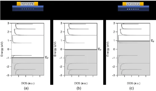
(b) divalent functionalization in "closed" configuration and (c) divalent functionalization in "open" configuration.
73
Figure II.19. Schematic representation of the resonant forms of
1,6-X-[10]annulene.
74
Figure II.20. (a) Transfer curves of pristine and covalent functionalized
SWCNTs and (b) representation of the hopping transport between functionalization induced gap states.
75
Figure III.1. Schematic representation of the electrode pattern in CNT-FET in
geometry 1.
81
Figure III.2. Schematic representation of the functionalization of oxidized
silicon substrate by APTES.
81
Figure III.3. Height AFM images of various concentrations of SWCNTs
deposited on Si/SiO2 substrates.
83
Figure III.4. Schematic representation of the fabrication process of
SWCNT-FETs (Geometry 1).
xxii
Figure III.5. AFM and SEM images of connected devices. 85
Figure III.6. AFM images and height cross-section of an individual SWCNT
and a CNT bundle connected between two electrodes.
86
Figure III.7. (a) Schematic representation of the electrode pattern in
CNT-FET geometry 2 and (b) optical microscopy image of the photolithography mask used for the design of electrode pattern.
87
Figure III.8. Fabrication process of multiple CNT-FETs on one single
SWCNT (Geometry 2).
88
Figure III.9. SEM image of a section of chip in geometry 2. 89
Figure III.10. Schematic representation of the electrode pattern in CNT-FET
geometry 3, used for sensing experiments.
90
Figure III.11. Proportion of connected devices for the three geometries of
devices.
92
Figure IV.1. Schematic representation of the Meerwein reaction between an
aryl diazonium salt and an alkene.
96
Figure IV.2. Radical chain mechanism for the covalent functionalization of
the carbon nanotubes with aryl diazonium salts.
98
Figure IV.3. Schematic representation of the addition of phenyl pairs on the
carbon nanotube surface.
99
Figure IV.4. Schematic representation of the possible cross-linking reaction of
aryl radicals on the carbon nanotube surface.
100
Figure IV.5. Schematic representation of the chemical pathway developed for
the deposition of metallic nanoparticles on the carbon nanotube surface.
102
Figure IV.6. Scheme of the chemical functionalization pathway developed for
the preparation of heterogeneous supported catalysts.
104
xxiii
films on Si/SiO2 substrates.
Figure IV.8. Raman spectra of pristine and functionalized (a) bulk SWCNTs
and (b) substrate-deposited SWCNTs.
107
Figure IV.9. High resolution N 1s XPS spectra of bulk-NO2-Ph-f-SWCNTs before and after treatment with various reducing agents.
112
Figure IV.10. High resolution N 1s XPS spectra of bulk-NO2-Ph-f-SWCNTs and substrate-deposited-NO2-Ph-f-SWCNTs before and after treatment with hydrazine monohydrate.
113
Figure IV.11. Anchoring of phosphine ligands on NH2-Ph-f-SWCNTs and coordination of [Ru5PtC(CO)14COD].
114
Figure IV.12. TEM image of NPs supported on bulk-SWCNTs and size
distribution of the nanoparticles.
119
Figure IV.13. Distribution of distances between two neighboring
nanoparticles.
120
Figure IV.14. SEM images of NPs supported on individualized SWCNTs. 120
Figure IV.15. Effect of covalent functionalization of sc-SWCNT in the ON
and OFF states.
124
Figure IV.16. Effect of hydrazine treatment on transfer curves of
functionalized sc-SWCNT-FET.
127
Figure IV.17. Comparison of I-VG curves of pristine sc-SWCNT and nanoparticles supported on sc-SWCNT, after thermal activation.
129
Figure IV.18. Histogram showing the distribution of the VG shift observed between p-SWCNTs and NPs/SWCNTs.
130
Figure IV.19. Transfer curves at each step of the preparation of bimetallic
Ru-Pt nanoparticles supported on SWCNTs.
132
xxiv
hydrosilanes on the surface of metal nanoparticles.
Figure V.2. Catalytic transformation of dimethylphenylsilane in
dimethylphenylsilanol with water.
146
Figure V.3. Schematic representation of the different nanoparticle precursors
and the heterogeneous supported catalysts obtained from them.
149
Figure V.4. Conversion curves of the hydrolytic transformation of
dimethylphenylsilane for Ru, Pt and Ru5Pt/MWCNTs catalysts.
156
Figure V.5. Recyclability tests for the conversion of dimethylphenylsilane in
dimethylphenylsilanol with water catalyzed by Ru/MWCNTs; Ru5Pt/MWCNTs and Pt/MWCNTs.
160
Figure V.6. TEM images of Ru/MWCNTs before and after 6 runs of catalysis. 162
Figure V.7. TEM images of Ru5Pt/MWCNTs before and after 6 runs of catalysis.
163
Figure V.8. TEM images of Pt/MWCNTs before and after 6 runs of catalysis. 164
Figure V.9. Histograms showing the size distribution of Ru/MWCNTs;
Ru5Pt/MWCNTs and Pt/MWCNTs before and after 6 runs of catalysis, as determined by TEM.
165
Figure VI.1. Schematic representation of (a) dichlorocarbene-f-SWCNTs; (b)
methylene-f-SWCNTs and (c) nitrene-f-SWCNTs.
179
Figure VI.2. Schematic representation of (a) 1,3-dipolar cycloaddition of
azomethyne ylide and (b) Diels-Alder cycloaddition of o-quinodimethane on a carbon nanotube sidewall.
180
Figure VI.3. Schematic representation of Bingel and Bingel-Hirsch addition
reactions.
181
Figure VI.4. Schematic representation of the Suzuki-Miyaura cross-coupling
reaction between an aryl halide and an aryl boronic acid, to form biaryl compounds.
xxv
Figure VI.5. Schematic representation of the general catalytic cycle for the
Suzuki-Miyaura reaction.
184
Figure VI.6. Schematic representation of the two pathways proposed to
describe the transmetalation step of the Suzuki-Miyaura reaction.
185
Figure VI.7. Schematic representation of the chemical pathway developed for
the heterogenization of homogeneous catalysts on the carbon nanotube surface.
186
Figure VI.8. Chemical pathway developed for the preparation of
homogeneous supported catalysts.
188
Figure VI.9. Schematic representation of the Suzuki-Miyaura cross-coupling
reaction between 4-iodotoluene and phenylboronic acid.
188
Figure VI.10. Thermograms (under nitrogen) of pristine and alkyne-divalent
f-SWCNTs.
189
Figure VI.11. Schematic representation of the divalent functionalization of
SWCNTs by Br-malonate and NO2-malonate.
191
Figure VI.12. Schematic representation of the two possible ways of Pd
complexes coordination on alkyne-divalent f-SWNCTs.
194
Figure VI.13. High resolution Pd XPS spectrum of Pd(0)-divalent f-SWCNTs. 195
Figure VI.14. Transfer curves of pristine-SWCNT, alkyne-divalent f-SWCNT
and Pd(0) complexes coordinated on divalent f-SWCNT.
197
Figure VII.1. Schematic representation of the experimental setup used for the
real-time experiments.
214
Figure VII.2. Images of the Au wire-bonds and the circuit board used for the
real-time electrical measurements.
215
Figure VII.3. Schematic representation of an electrolyte gated SWCNT-FET. 216
xxvi
Figure VII.5. Real-time electrical response of different CNT-FETs before and
after exposure to dimethylphenylsilane.
226
Figure VII.6. Schematic representation of the midgap states-induced two level
current fluctuations.
229
Figure VII.7. Real-time electrical response of device A6 upon exposure to
dimethylphenylsilane solutions of various concentrations.
231
Figure VII.8. Real-time electrical response of device C7 upon exposure to
dimethylphenylsilane solutions of various concentrations.
232
Figure VII.9. Evolution of the fluctuation frequency in function of the
dimethylphenylsilane concentration for devices A6 and C7.
233
Figure VII.10. Evolution of the CNT conductance when the
dimethylphenylsilane concentration is gradually increased.
235
Figure VII.11. Real-time electrical response of device A6 upon exposure to
dimethylphenylsilane highlighting the variation of the fluctuation rate over time.
238
Figure VII.12. Envisioned control experiment with trimethylphenylsilane. 239
Figure VII.13. Evolution of the electrical response of device C7 with the
dimethylphenylsilane concentration and catalyst deactivation.
LIST OF ABBREVIATIONS
AND SYMBOLS
AcOEt Ethyl acetate
a1, a2 Primitive vectors of the graphene lattice
AAS Atomic Absorption Spectroscopy AFM Atomic force microscopy
APTES (3-aminopropyl)triethoxysilane CBr4 Carbon tetrabromide
Ch Helicity vector
CNT Carbon nanotube
COD Cyclooctadiene
CVD Chemical vapor deposition dba Dibenzylideneacetone
DBU 1,8-diazabicyclo[5.4.0]-7-undecene
DCM Dichloromethane
DOS Density of states
DWCNT Double-walled carbon nanotube EA Elemental analysis
EDX Energy-dispersive X-ray spectroscopy
EF Fermi level
EtOH Ethanol
f-CNTs Functionalized carbon nanotubes FET Field-effect transistor
GC Gas chromatography
xxviii
ICP-AES Inductively coupled plasma atomic emission spectroscopy ICP-OES Inductively coupled plasma optical emission spectroscopy IDS Drain-source current IR (m) (s) (vs) (w) Infrared spectroscopy medium band strong band very strong band weak band
LA Laser ablation
MeCN Acetonitrile
MeOH Methanol
MS Mass spectrometry
MWCNT Multi-walled carbon nanotube NMR Nuclear magnetic resonance
NP Nanoparticle
o-DCB 1,2-dichlorobenzene p-CNTs Pristine carbon nanotubes PDMS Polydimethylsiloxane PEG Poly(ethylene glycol) PEI Poly(ethylene imine) PMMA Polymethylmethacrylate PPh3 Triphenylphosphine
PPNCl Bis(triphenylphosphoranylidene)ammonium chloride PTFE Polytetrafluoroethylene
PVDF Polyvinylidene fluoride RBM Radial breathing mode RIE Reactive ion etching RIE Reactive ion etching
xxix
RT Room temperature
SEM Scanning electron microscopy SMU Source measure unit
STEM-EDX Scanning transmission electron microscopy coupled with energy dispersive X-ray
SWCNT Single-walled carbon nanotube TEM Transmission electron microscopy TFA Trifluoroacetic acid
TGA Thermogravimetric analysis VDS Drain-source voltage
VG Gate voltage
XAS X-ray absorption spectroscopy XPS X-ray photoelectron spectroscopy XRD X-ray diffraction
"Information is not knowledge. The only source of knowledge is experience." Albert Einstein
ACKNOWLEDGEMENTS
Si la thèse est avant tout un cheminement scientifique, l'aboutissement de plusieurs années de recherche sur un sujet passionnant et prometteur, elle ne se limite pas qu'à cela. C'est aussi, et surtout, une véritable expérience humaine, parsemée de joies comme de déceptions, de bonnes nouvelles mais aussi d'embûches. Une thèse, c'est un apprentissage accéléré de la vie. Vous l'aurez compris, une thèse est déjà une aventure en soi, alors que dire d'une thèse en cotutelle... Malgré les difficultés quelquefois rencontrées au cours de ce périple, cette thèse a été enrichissante tant d'un point de vue scientifique qu'humain. Ce doctorat m'a permis d'apprendre à mieux me connaître et à découvrir mes forces et mes faiblesses. Mais un doctorat est loin d'être un travail solitaire. En effet, ce travail n'aurait pas pu être réalisé sans le soutien de nombreuses personnes.
J'aimerais tout d'abord remercier mes deux promoteurs, les professeurs Sophie Hermans et Richard Martel. Sophie, merci d'avoir accepté de mettre au point cette collaboration et d'avoir cru en moi. Richard, merci de m'avoir accueillie dans ton laboratoire au Canada, merci pour ta confiance, ta compréhension et tes conseils avisés, merci de nous transmettre à tous ton amour de la recherche. A deux, vous avez su m'apporter l'expertise et les moyens nécessaires à l'élaboration de cette thèse.
Je remercie également les membres de mon jury, qui ont accepté de lire cette thèse et de l'améliorer grâce à leurs précieux conseils et commentaires.
xxxiv
Cette thèse a fait appel à de nombreuses techniques instrumentales et infrastructures, qui fort heureusement sont gérées par diverses personnes. Je tiens donc à remercier Khalid pour son aide et son soutien à l'Université de Montréal, Christophe et Alireza pour leurs enseignements des techniques de salle blanche, Michel Genet et Pierre Eloy pour leur soutien en XPS et Jessica Venicx pour la gestion du magasin Lavoisier. Enfin, je voudrais remercier Jean-François Statsyns. Jeff', merci pour ton aide et ton soutien, merci aussi pour ta bonne humeur. Les pauses café ne seraient pas pareilles sans toi. Merci aussi à Jacqueline Boniver, toi qui est toujours dévouée pour nous aider à surmonter les démarches administratives.
Je tiens également à remercier tout particulièrement les personnes qui ont contribué à l'élaboration de ce travail. Delphine, merci pour ton aide si précieuse, à Montréal, puis à New York. Merci d'avoir pris le temps de me faire découvrir un petit peu le monde de la physique. Sans cette collaboration, le projet n'en serait pas là, alors du fond du cœur, merci ! Je te souhaite beaucoup de succès dans ta carrière académique qui est sur le point de débuter. Dhan, merci d'avoir été un stagiaire incroyable ! T'encadrer a été vraiment un plaisir, et même si le projet graphène n'a pas abouti comme on l'espérait, "we finally dit it!". Je te souhaite le meilleur pour la suite ! Merci aussi à Sébastien, stagiaire IPL, pour sa bonne humeur et son travail qui a permis d'ouvrir des portes en vue de la catalyse.
I also would like to acknowledge Colin Nuckolls for offering me the great opportunity to join his lab at Columbia University for a few months. My thanks also go to Scott, Nathan, Sefi, and particularly to Jason and Delphine (again!) for their active collaboration on the sensor project. Thanks also to Jen for her communicative cheerfulness!
xxxv Merci aussi à tous les membres de mon labo belge. Merci à Charly, les deux Nath, Nico, Antoine, Anaëlle, Nadya, Dodji, Samuel et Sébastien. Je remercie tout particulièrement Francis... co! pour son soutien et sa gentillesse, Anto pour sa bonne humeur, Tommy pour les nombreux moments passés ensemble, dans et en-dehors du labo, qui ont vu naître une réelle amitié, et Flo, avec qui j'ai partagé tout mon parcours universitaire, et que j'espère revoir par la suite, malgré la distance ;-).
Je tiens également à remercier tous les membres du groupe Martel. Merci à Nathalie pour son accueil au sein du labo, à François et Delphine pour leur gentillesse, leur aide et leurs nombreuses discussions scientifiques. Merci aussi à Minh, Philippe, May, Pierre, Maxime et Benoit. Merci tout particulièrement à Saman, Dhan et Natasha pour la bonne ambiance au sein du bureau.
Merci également à Patrick et Annie-Claude, ma "famille du Québec", pour leur accueil, leur gentillesse, et les nombreux bons moments partagés avec eux. Les soirées hockey, la musique de Patrick et les cocktails d'Annie-Claude, le montage de meubles Ikea jusqu'au bout de la nuit, la gentillesse de vos familles respectives, sans oublier ce nouvel an mémorable en Beauce, ne sont qu'une petite partie des nombreux souvenirs que je garde de mes passages à Montréal à vos côtés. J'espère de tout cœur que ce n'est que le début d'une vraie amitié, et que malgré la distance, nous aurons l'occasion de nous revoir !
Enfin, je tiens à remercier Jean-Pierre, pour l'amour et le soutien qu'il a su m'apporter au quotidien. JP, merci pour tes encouragements et ton soutien. Tu as toujours su être présent pour moi, même lorsqu'un océan nous séparait, et je ne t'en remercierai jamais assez. Sans toi, je ne serais pas devenue la personne que je suis aujourd'hui. Merci pour tout !
CHAPTER I - INTRODUCTION
Abstract
This thesis aims at exploring ways to detect dynamically chemical reactions at the level of single events. For this purpose, carbon nanotubes constitute ideal candidates, since their electrical properties are very sensitive to slight modification of their environment. As a result, carbon nanotube based sensors are appropriate tools to probe chemical reactions in real-time. In this thesis, we selected catalysis for its ability to induce charge transfer reactions at the surface of the active sites.
This chapter intends to introduce the context of this thesis. Hence, the first part of this introduction will be devoted to sensors, a technology which is omnipresent in our modern world. We will particularly focus on current advances in the field of carbon nanotube-based sensors. A second section will provide an overview of the techniques commonly used for in situ detection of catalysis. Our attention will be focused on operando catalysis, a field in constant development. Finally, this chapter will be concluded with a description of the thesis objectives and an outline of the present manuscript.
The key concepts required for the understanding of this thesis will be developed further in the next chapter.
2
I.1 Sensors
Sensors are inherent parts of the world. They can be either natural or man-made. Humans are endowed with five senses: hearing, sight, smell, taste and touch. These five senses can be regarded as natural sensors, enabling us to detect various stimuli.1 The perception of sound is based on
the transformation of vibration waves to electrical nerve impulses. This transformation is ensured by the ear, while the interpretation of the electrical nerve signal is done by the brain. In a similar way, the sight results from the capacity of the eyes to generate electrical nerve impulses from the visible light rays reflected from objects. The brain is then able to recreate an image from these electrical impulses. Smell and taste perceptions are ensured by sensory organs: olfactory receptors and taste buds, respectively. Finally, touch results from the stimulation of neural receptors located on the skin. Certain animals and plants also possess other natural sensors, which act as detection methods for their protection. The chameleon changes its color as camouflage,2 while carnivorous plants are
able to trap their prey, thanks to the presence of trigger hairs.3
Sensors have also been fabricated by humans. In 1714, Fahrenheit invented the mercury thermometer,4 which can be viewed as a temperature
sensor: upon temperature variation, the mercury contained in this thermometer indeed dilates or compresses. As a consequence, the mercury level changes, enabling us to detect the temperature change.
Today, more than ever, our daily lives are surrounded by sensors. Our houses are equipped with smoke detectors, room thermostat, motion and light detectors, alarm systems equipped with windows and doors sensors, etc.5 Modern cars are equipped of up to hundreds of sensors, such
3 as tire pressure detector, oil and fuel level gauges, automatic doors and windows, cruise control, rain detectors, parking assistance, etc.5 Often
without realizing it, we use other sensors everyday: when using household appliances, when passing through automatic doors when entering a commercial center, when pushing on touch-sensitive elevator buttons, when using our smartphones, etc. Sensors are also present in very common medical devices, such as glucose and insulin test systems, ethyl tests, blood pressure tests and pregnancy tests.5
This non-exhaustive list of practical applications of sensors emphasizes the importance of these devices for innovation progress. As a consequence, many efforts are placed on the development of improved sensors.
I.1.1 Definition and characteristics
A sensor can be defined as a device that responds to a chemical, physical or biological event or stimulus by generating a processable signal, most of the time electrical or optical (Figure I.1).1,5,6 Generally, a sensor is
composed of a sensitive element and a transducer. As it name suggests, the sensitive element is able to detect a physical, chemical or biological event, while the transducer converts this event in a signal that is readable by an observer or an instrument.5,7
Practically, different transduction processes can be involved in sensors. The processes are based on various physical phenomena, such as optical, electrical, mechanical and magnetic effects. Depending on the nature of the detected input, the sensor is called either a chemical sensor, a physical sensor, or a biosensor.
4
Figure I.1. Schematic representation of the sensing process: the sensor detects a
biological, physical or chemical stimulus; this measurement is then converted in a readable electrical or optical signal. Figure inspired from McGrath et al.7
To be efficient, a sensor must meet several requirements such as
sensitivity (i.e. the variation of the output response induced by a unit
change of the input5,7,8) and selectivity (i.e. the ability to detect a specific
analyte, without interferences of other analytes present during the measurement5,8). In addition, a sensor should be able to respond quickly to
the external stimuli.
I.1.2 Nanotechnology-enabled sensors
Innovation in the field of sensors points toward the conception of sensing arrays composed of multiple sensing devices, able to selectively detect multiple analytes. Additionally, these sensing arrays are expected to be miniaturized. In this respect, nanotechnology appears to be a powerful tool.6,8 Nanotechnology can be defined as the understanding and control of
the matter at dimensions on the order of nanometer (i.e. comprised between 1 and 100 nm).9 The interest of nanotechnology lies in the ability
5 to create materials exhibiting novel properties compared to their micro- or macroscopic analogues.9,10 At the nanoscale, materials possess high
surface-to-volume ratios, favoring surface reactions, such as the detection processes implied in chemical sensors. Moreover, when dealing with materials at the nanoscale, unique optical, electrical, mechanical and magnetic properties are obtained.6,10 Since these properties are generally
involved in the transduction process of sensors, nanotechnology offers the possibility to design novel sensor systems, exhibiting enhanced sensitivity and selectivity.6,11
Among the possible applications of nanotechnology for sensor design, semiconducting nanomaterials can be used to probe the presence of specific analytes through conductance modification. One-dimensional nanomaterials, such as carbon nanotubes (CNTs) or metal-oxide nanowires, can be advantageously used for this application. Thanks to their unidimensionality, these materials exhibit enhanced sensitivity, compared to 2D materials, as depicted in Figure I.2. Moreover, these nanomaterials can be implemented into high-density sensing arrays, thanks to an appropriate lithographic pattern.
Figure I.2. Schematic representation of the localization of the electrical effects induced
in 1D-nanomaterials, compared to 2D-nanomaterials. Figure inspired from 6,12 .
6
I.1.3 Carbon nanotube-based sensors
I.1.3.1 Interest of carbon nanotubes for sensors
To date, thousands of studies have investigated the usability of carbon nanotubes for the design of chemical sensors. Carbon nanotubes indeed constitute ideal candidates for this application, since they exhibit remarkable electronic properties, which are extremely sensitive toward chemical changes.11 In addition, CNTs also possess an extremely high
aspect ratio, i.e. the ratio between their length and diameter. This feature facilitates their assembly in electronic devices, for an efficient detection of the chemical sensing.
Carbon nanotubes also possess extremely high surface area (ca. 1600 m2g-1 for single-walled carbon nanotubesi).13 This property, coupled with
the fact that each atom is exposed at the surface (at least for SWCNTs), makes them particularly sensitive to variation of their chemical environment.11 Their nanometer scale makes them particularly suitable for
the detection of biological and molecular events. In addition, their all-carbon composition ensures an appropriate match for organic and biological molecules.14
Lastly, many efforts have been placed during the last decades on the functionalization of these materials. Such functionalization enables the
i Carbon nanotubes can be distinguished according to their number of concentric carbon
cylinders: CNTs composed of only one carbon cylinder are called single-walled carbon nanotubes (SWCNTs), while CNTs composed of multiple concentric cylinders are known as multi-walled carbon nanotubes (MWCNTs).
7 design of very selective sensors, by anchoring specific receptor sites on carbon nanotubes.
I.1.3.2 Incorporation of carbon nanotubes in sensors
A convenient approach for the preparation of carbon nanotube-based sensors consists in integrating them into field-effect transistors (FETs). As will be deeply discussed in the next chapter, the electronic properties of CNTs allow them to be used as semiconducting channels in such electronic devices. These CNT-FETs are particularly adapted to probe environment modification, since such changes induce modifications of the nanotube electrical conductivity. Two different effects can be induced by analyte-CNT interactions: (i) charge transfer from analyte to the analyte-CNT can induce a modification of the charge carrier concentration in carbon nanotubes, which directly impacts their conductivity11,13,14 and (ii) adsorption of
analyte species can also introduce scattering sites across the nanotube, hence reducing the charge carrier mobility.11,14,15 These two effects directly
impact the nanotube conductivity. As a consequence, measuring the nanotube conductance enables to probe chemical changes in their environment.
The following section gives a brief and non-exhaustive overview of the applications of carbon nanotubes in sensing devices which have been reported so far.
It is worth noting that, besides these above-described major advantages of carbon nanotubes for sensing applications, the commercialization of carbon nanotube-based sensors is limited by the cost, reproducibility and stability of the fabricated sensors. There is indeed a need for controlled synthesis of CNTs, which would lead to reproducible
8
batches of CNTs. Notwithstanding the achievements developed with CNT-based technologies, substantive research efforts still need to be placed on the fabrication of reproducible and high-performance electronic devices.16
Despite these limitations, carbon nanotubes are particularly suited for sensing applications due to their open-structure, high sensitivity, time resolution, versatility, etc. Therefore, carbon nanotube-based sensors are mostly interesting as a tool to carry fundamental research, without foreseeable industrial perspectives in the near term.
I.1.3.3 State of the art
I.1.3.3.1 Gas and vapor sensors
Gas sensors are of critical importance for many applications, going from environmental considerations, toxicity control, medical applications to explosives detection for military and defense applications. Such applications require extremely sensitive and selective sensors able to operate at room temperature, three critical parameters that can be met by the use of carbon nanotubes. For this reason, numerous studies have investigated the application of carbon nanotubes in gas sensing.11,12,17–24
The ability of using carbon nanotubes for gas sensing was demonstrated for the first time in 2000, when J. Kong et al. observed that the conductance of CNTs could be significantly altered (i.e. decreased or increased) by exposure to ammonia (NH3) or nitrogen dioxide (NO2).25
Figure I.3a shows the sharp decrease of CNT conductance after exposure to NH3. On the other hand, exposure to NO2 resulted in a large increase of the nanotube conductance (Figure I.3b). These conductance changes were attributed to charge transfer between the nanotube and the exposed gas.
9 NH3 indeed possesses a lone pair of electrons that can be donated to the nanotube, resulting in n-doping, decreasing the intrinsic p-conductance of the nanotube. On the contrary, NO2 is an electron-withdrawing molecule, and its exposure to CNT sensor results in a p-doping, increasing the nanotube conductance.25
(a) (b)
Figure I.3. Electrical response of a CNT-FET sensor to exposure of (a) NH3 and (b) NO2 gas. Reprinted from
25
with permission from AAAS,
http://science.sciencemag.org/content/287/5453/622.
A few weeks later, P.G. Collins et al. reported the extreme sensitivity of carbon nanotube electronic properties toward oxygen exposure.26 As depicted in Figure I.4, the CNT resistance decreased by
10-15 % upon exposure to air instead of vacuum. Independent experiments performed with the different constituting gas of air demonstrated that this effect is due to the presence of oxygen. This effect was later attributed to charge transfer between adsorbed oxygen/water redox couple and carbon nanotubes.26,27
Figure I.4. Variation of the electrical resistance of a CNT film under exposure to
vacuum or air. Reprinted from 26
with permission from AAAS,
10
In 2003, K. Someya et al. observed changes in electrical response of individual CNT-FETs upon exposure to various alcohol vapors.28
Depending on the nature and partial pressure of the alcohol, various electrical responses were observed (Figure I.5), which was promising for the preparation of specific sensors.
Figure I.5. Electrical response of an individual CNT-FET upon exposure to various
alcohol vapors. Reprinted with permission from 28
. Copyright © 2003 American Chemical Society.
Despite these tremendous advances for the detection of gases using carbon nanotubes, these materials sometimes lack of sensitivity towards common gases such as hydrogen, methane, carbon monoxide and hydrogen sulfide. Decoration of CNTs with specific functions or metal nanoparticles was shown to enhance the sensor sensitivity and selectivity. Figure I.6 depicts the influence of various metal on the sensitivity of CNT-based sensors toward NH3 and NO2 exposure.29 As can be seen, the
electrical response of Pt/CNTs toward NH3 was significantly improved compared to bare CNT-based sensors. In a similar way, addition of Au or Pt nanoparticles on CNT sensors significantly improved its electrical response on NO2 exposure. This sensitivity increase was explained by an intimate interaction between the detected gas and the metal: the gas likely
11 dissociated at the metal surface, which induced the decrease of the metal work function, and a charge transfer between the metal and the nanotube.29
(a) (b)
Figure I.6. Electrical response of bare-MWCNTs film and metal decorated MWCNTs
films on 10 minute exposures to (a) NH3 and (b) NO2. Reprinted from 29
with the permission of AIP Publishing.
The detection of H2 by metal nanoparticle decorated carbon nanotubes has also extensively been investigated.30–36 While bare CNTs do
not show sensitivity to H2, Pd decorated CNTs are able to detect hydrogen in proportion as low as 10 ppm.33 Pt particles also enhance CNT sensitivity
toward H2.31,34,37 In a similar way, Pd and Sn decorated CNTs were used to
detect the presence of methane,37,38 Pd nanoparticles supported on CNTs
were shown to be efficient for the detection of H2S37 and Rh was used to
modify CNTs for the detection of CO.37 Table I.1 summarizes the main
12
Table I.1. Summary of the main metal-decorated carbon nanotube-based gas sensors.
Gas Nature of the
metal CNT material H2 Pd Individual SWCNT-FET32 Thin films of MWCNTs31 Network SWCNTs-FET30 Thin films of SWCNTs33,35 Pt Theoretical study34 Thin films of MWCNTs31 Individual SWCNT-FET37 CH4 Sn Individual SWCNT-FET 37 CO Rh Individual SWCNT-FET 37 Au Network of SWNCTs39 H2S Pd Individual SWCNT-FET37 Au Network MWCNTs-FET40 NH3 Pt Thin films of MWCNTs29 Au Network of SWNCTs39 NO2 Pt Thin films of MWCNTs29 Au Thin films of MWCNTs 29 Network of SWNCTs39 I.1.3.3.2 Biosensors
The detection of biological species is of critical importance for biomedical diagnostics. Since most of the biological and chemical processes involve electrostatic interactions, electronic detection emerges as a powerful alternative to optical detection methods.15 Given the low
dimensions of biological species − about 10 nanometers for proteins, while DNA possesses a diameter of about 2 nm only − the use of nanometer scale sensitive materials, such as carbon nanotubes, is desirable.13,15,41–47
13 The next sections briefly describe selected examples showing the scope of carbon nanotube-based biosensors for various biomedical applications.
a) Protein detection
The interaction between streptavidin and carbon nanotubes has been investigated with carbon nanotube-based bioelectronic sensors.48 In this
experiment, CNT-FETs were incubated in a buffer solution containing streptavidin and the current passing through the nanotube was measured during the incubation. As depicted in Figure I.7, the current increased gradually immediately after the addition of the protein in the solution. This current shift was interpreted as resulting from interactions between amine functions of streptavidin and carbon nanotube surface, while the gradual variation was explained by the progressive formation of a monolayer of proteins.48
Figure I.7. Detection of streptavidin with carbon nanotube-based sensor: (left)
representation of the interaction between the streptavidin and the CNT; (right) current versus time response of a CNT-FET device incubated in a solution containing streptavidin. The arrow indicates the addition of the streptavidin in the solution. Adapted with permission from 48
. Copyright © 2004 American Chemical Society.
In order to increase the sensor sensitivity and selectivity, Star et al. integrated biotin-functionalized carbon nanotubes in field-effect transistor, for the selective detection of streptavidin.49 The nanotubes were
14
(PEI), provided amino groups for the anchoring of biotin functions, while the second one, poly(ethylene glycol) (PEG), prevented the non-specific adsorption of species on the CNT surface during the sensing experiment. As depicted in Figure I.8, the nanotube conductivity was significantly decreased by the presence of the specific protein. This conductivity loss was attributed to geometric deformation induced by the formation of the biotin-streptavidin complex, leading to scattering sites on the nanotube, hence decreasing its conductivity.49
Figure I.8. (Left) Schematic representation of a biotin-functionalized CNT sensor for
the selective detection of streptavidin. (Right) Electrical response of the device in absence and presence of streptavidin. Adapted with permission from 49
. Copyright © 2003 American Chemical Society.
b) Detection of specific ligand-receptor interactions
In a similar way, carbon nanotubes have been functionalized to anchor specific receptor sites, able to selectively detect other biomolecules.50–52
For example, the specific antigen-antibody interaction has been used to design CNT-based biosensors.53,54 Li et al. investigated the specific
recognition of a prostate specific antigen (PSA), a marker for the presence of prostate cancer, with modified carbon nanotube-based sensors.53 First,
15 functions. This linker was then used for the coordination of PSA antibody. Finally, these PSA antibody-modified CNTs were integrated into electronic devices, and incubated in a buffer solution. As shown in Figure I.9, the introduction of the specific PSA antigen resulted in a decrease of the nanotube conductivity, in response to the antigen-antibody interaction. On the contrary, when the sensor was incubated in a solution containing bovine serum albumin (BSA), the sensor did not show any response to this protein. This result indicated the selectivity of this sensor for the desired PSA antigen, thanks to the prior functionalization of the nanotubes. Moreover, this system allowed to detect PSA in amount as low as 50 ng/ml, which is the level expected for clinical diagnosis of prostate cancer.53
Figure I.9. (Left) Schematic representation of a CNT-based sensor designed for the
specific recognition of a prostate specific antigen (PSA). Dotted line shows the anchoring and desorption of PSA on its specific antibody. (Right) Electrical response of the device in presence of the specific PSA antigen, and in presence of the non specific BSA protein. Adapted with permission from 53
. Copyright © 2005 American Chemical Society.
Based on the same principle, carbon nanotube-based biosensors have proved to be efficient for the detection of viruses, with direct applications for medical diagnosis.55–57 Singh et al. demonstrated the possibility of
detecting influenza virus H1N1 with carbon nanotubes.57 Viral antibodies