To link to this article : DOI:
10.1016/j.ces.2016.08.039
URL :
http://dx.doi.org/10.1016/j.ces.2016.08.039
O
pen
A
rchive
T
OULOUSE
A
rchive
O
uverte (
OATAO
)
OATAO is an open access repository that collects the work of Toulouse researchers and
makes it freely available over the web where possible.
This is an author-deposited version published in :
http://oatao.univ-toulouse.fr/
Eprints ID : 16085
To cite this version :
Aviziotis, Ioannis G. and Cheimarios, Nikolaos and Duguet,
Thomas and Vahlas, Constantin and Boudouvis, Andreas G. Multiscale modeling
and experimental analysis of chemical vapor deposited aluminum films : Linking
reactor operating conditions with roughness evolution. (2016) Chemical
Engineering Science, vol. 155. pp. 449-458. ISSN 0009-2509
Any correspondence concerning this service should be sent to the repository
administrator:
[email protected]
Multiscale modeling and experimental analysis of chemical vapor
deposited aluminum films: Linking reactor operating conditions
with roughness evolution
Ioannis G. Aviziotis
a,b, Nikolaos Cheimarios
c, Thomas Duguet
b, Constantin Vahlas
b,
Andreas G. Boudouvis
a,naSchool of Chemical Engineering, National Technical University of Athens, Heroon Polytechniou 9, 15780 Zografou, Greece bCIRIMAT, CNRS, Université de Toulouse, 4 alleé Emile Monso, BP 44362, 31030 Toulouse cedex 4, France
cScienomics SARL, 16 rue de l'Arcade, 75008 Paris, France
H I G H L I G H T S
!Experimental and computational analysis of Al CVD from DMEAA. !Multiscale computational framework
for the roughness evolution. !Direct comparison to experimental
data with good agreement. !Effective sticking coefficient
includ-ing chemical information.
!Prediction of electrical resistivity through roughness simulations.
G R A P H I C A L A B S T R A C T Keywords: Multiscale modeling Sticking coefficient Aluminum CVD RMS roughness Electrical resistivity
a b s t r a c t
When composition and crystallographic structure remain constant, film properties mainly depend on microstructure and surface morphology. In this case, the proper modeling of a growing film allows linking the final surface features with the operating conditions at the reactor scale which in turn enables the control of the properties of the final film. In this work, an experimentally supported, coarse-grained, multiscale framework is applied for the modeling of the surface roughness of aluminum thin films processed by chemical vapor deposition from dimethylethylamine alane. The multiscale framework is developed by linking macroscopic transport phenomena based on continuum mechanics models with nanoscale surface events which are simulated stochastically. The model reproduces experimental data successfully, thus validating the method with good statistics. Finally, modeling of surface roughness enables the estimation of the electrical resistivity in good agreement with corresponding measurements.
1. Introduction
The rapid advancement of thin films and coatings technologies promoted their usage in a wide range of applications, e.g. micro-electronic devices, solar cells, or biomedical products. Aluminum
(Al), the third most abundant element on the EarthÕs crust, is used for the fabrication of integrated circuits due to its low electrical resistivity (Lee et al., 2012,2013,2014). Moreover it is resistant to corrosion (Hamasha et al., 2011) and to electromigration (Tan and Roy, 2007). In addition it can be combined with other elements for the formation of Al-based intermetallics with many degrees of freedom for the exploration of original properties (Kadok et al., 2015). Various methods are developed for the production of Al and
nCorresponding author.
Al-containing thin films, among which chemical vapor deposition (CVD) combines high growth rates and conformal coverage of complex surfaces (Thomann et al., 2011). However CVD processed Al films suffer from a rough microstructure, despite efforts made to attenuate it (Vahlas et al., 2001).
Microstructural characteristics depend on process conditions (surface temperature, pressure, flow rates, etc). In turn, they im-pact the targeted properties such as electrical resistivity ( Timal-shina et al., 2015), hydrophobicity (Bormashenko et al., 2006; Bravo et al., 2007) and adsorption of proteins (Rechendorff et al., 2006;Zhdanov et al., 2008). Consequently, the technological im-plementation of such process with regard to targeted specifica-tions requires the establishment of a robust relation between process parameters and films microstructure, e.g. surface rough-ness. This can be met through the modeling of the CVD process with the roughness as an output.
For most CVD processes, transport phenomena can be de-scribed by macroscopic conservation equations for momentum, mass, energy and species. Gas phase and surface chemistry are described in these models by means of kinetic schemes consisting of elementary reactions. However, the continuum description breaks down as the length scale approaches the surface level. Modeling the surface characteristics, e.g. roughness at the same length scale used to model the bulk phase of a reactor, leads to the loss of any structural information of the evolving surface (Barbato et al., 2007). The limitation on the use of the continuum models for the description of surface processes and the evolution of the surface topography during film growth on initially flat surfaces has led to the development of stochastic kinetic Monte Carlo (kMC) modeling (Battaile and Srolovitz, 2002; Cavallotti et al., 2004; Chaterjee and Vlachos, 2007;Collins et al., 2008;Gillespie, 1977, 2001; Katsoulakis and Vlachos, 2003) and multiscale modeling (Cheimarios et al., 2011;Christofides et al., 2008;Crose et al., 2015; Hu et al., 2010; Lam and Vlachos, 2001; Lou and Christofides, 2003;Rodgers and Jensen, 1998;Zhang et al., 2010). The rates of surface processes, such as adsorption, desorption and surface mi-gration, which are necessary for the kMC model, can be provided
by experimental data or from molecular dynamics (Rapaport,
2004) and by density functional theory calculations (Zorn et al., 2009).
In multiscale models, the reactor scale is linked to the surface level through the feeding of computational information. The first efforts for linking deterministic macroscopic models with sto-chastic kMC models have been made for the CVD of diamond (Battaile et al., 1998; Srolovitz et al., 1997), while tries for the coupling of the two different scales are reported for CVD processes taking place in a vertical reactor without using any specific che-mical system (Raimondeau and Vlachos, 2000). In the latter, due to the low concentration of the precursor, the continuum equations are solved decoupled. At the macroscopic level, the one-dimen-sional partial differential equations provided by the similarity transformation of the mass, momentum, energy and species transport equations are used, whereas only one node of the computational domain is chosen to be used for the kMC simula-tions. The same model is also used byLou and Christofides (2003) for the estimation of the surface roughness, where the estimated roughness from the multiscale framework is used as an input to a proportional-integral (PI) controller for the successful regulation of the surface roughness at the desired value.
Multiscale simulations of the CVD of Si have been performed (Masi et al., 2000). In this system, only the species transport equations are solved at the macroscopic level and the developed kMC model does not take into account the formation of dimers which is a characteristic of Si surfaces. The linking between the two scales is performed through the deposition rate, by assuming that it remains unchanged regardless the scale. The same
assumption has also been used in a different work for the CVD of diamond (Grujicic and Lai, 2000). These studies confirmed that process conditions, such as deposition temperature and mass fraction of the precursor at the inlet of the reactor, have a sig-nificant effect on the deposition rate and on the surface roughness of the films (Lam and Vlachos, 2001).
More recently, the coupling of different length scales has been attempted for the multiscale modeling of the deposition of Si (Barbato et al., 2007, Cavallotti et al., 2004, 2005). There, the macroscopic model is integrated based on the governing con-servation equations, while the kMC model takes into account the adsorption of multiple molecules and the formation of dimer structures. Finally, multiscale frameworks are also developed for plasma-enhanced CVD (PE-CVD); for instance, the formation of Si thin films for solar cells (Crose et al., 2015) involves a macroscopic model that consists of the 2-dimensional solution of the con-tinuum equations and a hybrid kMC which accounts for more events on the surface, such as hydrogen abstraction (Tsalikis et al., 2013).
Multiscale frameworks offer a basis for the control of the op-erating conditions at the reactor scale through regulation of sur-face micro-/nano features such as roughness and porosity. In Christofides et al. (2008), the multiscale model considers substrate temperature as the manipulated input parameter for the tailoring of the surface roughness. In Hu et al. (2010), film thickness, roughness and porosity are simultaneously regulated using the concentration of the precursor at the inlet of the reactor as the manipulated parameter. Finally, precursor concentration and modulation of the substrate temperature are used as inputs in Crose et al. (2015)for the control of the physisorption of surface radicals and consequently for the control of film growth rate and roughness.
The multiscale computational framework described in the present contribution is based on the assumption which has al-ready been adopted in the past (Masi et al., 2000) according to which the deposition rate remains unchanged regardless the considered scale. At the macroscopic level, steady-state, 3D si-mulations are performed for the solution of the governing equa-tions and the computational information which is fed to the na-noscale is the mass fraction of the Al precursor at the surface. The derived kMC algorithm for the description of the microscopic state is developed based on an existing model (Lam and Vlachos, 2001). As a first approach to our experimental measurements and without ignoring the crystallinity and the structure of the devel-oped Al films, we choose to work with a coarse-grained kMC model. The coarse-graining lies in the usage of a simple cubic lattice despite the fcc structure and the (111) orientation of the obtained Al films. The implementation of such an approximation, results in a reduced number of interactions between the surface atoms (five instead of twelve, respectively) and consequently in a reduced computational effort, without sacrificing accuracy. In-dicatively, the CPU time required for kMC simulations of the Al surface is approximately 3 h; a similar to the presented kMC model applied inVlachos (2008), requires 73 min of CPU time, for a 40 " 40 lattice and without incorporating migration events. Ac-celeration of the computations can be achieved (1.8 min of CPU time, for the latter case) when appropriate methods, such as the
τ
-leap method, are applied (Gillespie, 2001; Vlachos, 2008). In contrast, at the nanoscale level, exact atomistic simulations in-stead of coarse-grained computations are used for the detailed reproduction of the surface microstructure but highly increase the computational requirements. An example is the homoepitaxial growth of Ag on Ag (111) and the diffusion of Ag monolayer islands on Ag (111) reported byLatz et al. (2012); in this model, the de-tailed crystallographic structure of Ag along with interactions among second nearest neighbors is used to perform on the flysimulations for the reproduction of the exact Ag (111) growth. This type of simulations yields an almost hundredfold increase of the computational requirements and self-learning models are applied to reduce the high computational cost (Latz et al., 2012). It will be shown that, within these limitations, the simulated surfaces match well the experimentally determined surface features of the films. The microscopic algorithm does not explicitly include chemical reactions on purpose; indeed, the chemical information is in-corporated in the effective sticking coefficient through a fitting process that correlates this parameter with surface temperature. By fitting the microscopic sticking coefficient to the surface tem-perature through the macroscopic Al deposition rate (it is recalled that the deposition rate remains unchanged regardless the scale of simulation), we virtually integrate all the steps involved in the chemical reactions (precursor adsorption/desorption, decomposi-tion, products adsorption/desorpdecomposi-tion, etc.) to end up with an ef-fective sticking coefficient for Al atoms. This particular treatment of the sticking coefficient allows performing fast and accurate computations for the CVD of Al by implementing a procedure which appears as a purely physical one; i.e., involving single Al atomic events only.
Through this framework, we investigate the CVD of Al films from dimethyl-ethylamine alane (DMEAA) by focusing on growth rate and the surface roughness and we compare our computa-tional results with experimental data obtained in similar condi-tions. DMEAA exhibits relatively high vapor pressure at room temperature facilitating its transport into the reactor, and low process temperature allowing deposition on thermally sensitive substrates. DMEAA processed Al films are oxygen/carbon-free (Yun et al., 1998; Yun and Rhee, 1998) and present smoother micro-structure than alternative Al precursors such as triisobutyl alu-minum (Delmas and Vahlas, 2007). The reaction scheme and ki-netics of DMEAA has been extensively studied in previous works (Gladfelter, 1993; Jang et al., 1998; Venkateswaran et al., 1996; Xenidou et al., 2010;Yun et al., 1998) and several reaction paths have been proposed (Kim et al., 1996; Nakajima et al., 2003; Simmonds et al., 1994;Xenidou et al., 2007;Yun et al., 1998).
Previous works dealing with the CVD of Al from DMEAA focus on the investigation of the kinetic mechanisms and not on the evolution of the microstructure (Aviziotis et al., 2015;Delmas and Vahlas, 2007;Venkateswaran et al., 1996). Thus, it is important in the present case to develop a computational framework which will simulate the surface evolution and reproduce the experimentally determined roughness. As a consequence, the tailoring of final properties of interest is enabled. The evolution of the electrical resistivity (whose low values for a metal are appealing for nu-merous applications) as a function of process conditions through their impact on the microstructure will be used in this manuscript as a paradigm of this relationship.
The paper is organized as follows: first, we briefly present our experimental work and then, we detail the multiscale framework which enables the simulations at the surface level. Upon the de-scription of the computational framework, we show the results provided by this analysis and we compare them with the corre-sponding experimental measurements. Finally, we show the de-pendence of the electrical resistivity of Al thin films on surface roughness and discuss the main findings of this work.
2. Experiments
The CVD of Al thin films is performed in a vertical, cylindrical, stagnant flow, warm wall, stainless steel reactor which has been
previously described in detail (Xenidou et al., 2010).
20 " 10 " 1 mm3silicon coupons were cut from 4″ Si (100) wafers
(Sil'tronix). They are etched in a (1 ml HF:10 ml H2O) bath for
1 min, sonicated in an acetone and ethanol bath for 5 min, dried in Ar flow and baked in a furnace at 60 °C for 20 min. In each ex-periment three substrates are placed horizontally at the center (0 mm), the edge (24 mm) and at an intermediate location (17 mm), on a 58 mm diameter susceptor (substrate holder) he-ated by a resistance coil gyred just below the surface, where a regulating thermocouple is also attached. Surface temperature Tsis
calibrated under primary vacuum by attaching a second thermo-couple to the surface of a dummy Si coupon. In the presence of a perforated shower plate which is facing the substrates, a homo-geneous gas distribution is ensured, in contrast to a large re-circulation zone that sets in when the shower plate is absent. The 60 mm diameter shower plate consists of 1450 holes of 0.76 mm diameter each. DMEAA, is supplied by NanoMePS in a specifically designed glass bubbler equipped with a 3-valve stainless steel bypass system. It is maintained at 3 °C permanently; i.e. below the freezing point of the compound, thus strongly limiting its de-gradation (Jang et al., 1998). It is thermally regulated to 7 °C during experiments. At this temperature, the partial pressure of DMEAA is 0.7 Torr (Jang et al., 1998). Pure nitrogen (99,998%, Air Products) is fed through computer-driven mass flow controllers. Experiments are performed in fixed conditions, namely total pressure of the reactor Ptot¼10 Torr, thermal regulation of the lines Tlines=100 C° and of the walls of the reactorTwalls=75 C° , while the N2dilution
gas flow (QN dilution2, )and the N2carrier gas flow through the
pre-cursor(QN prec2, )equal 305 and 25 standard cubic centimeters per
minute (sccm), respectively. Considering the relation proposed by Hersee and Ballingal (1990), these conditions yield a maximum flow rate Qprecof DMEAA in the input gas, equal to 2 sccm.
Independent experiments are performed at eight different Ts, in
the range 139–241 °C. Deposition time is 1 h and deposition rate is evaluated directly by weight difference of the substrates before and after deposition, using a microbalance (Sartorius) with
710
μ
g accuracy. Three independent weight measurements arecarried out before and after the experiment and their average value is considered. The maximum (minimum) deviation from this average value is estimated by the difference between the mini-mum (maximini-mum) value before the experiment and the maximini-mum (minimum) value after the experiment. Hence, the average value of the weight lies always within the limits of the maximum and minimum deviations.
Surface roughness is determined with an optical interferometer (Zygo NewView 100) allowing measurements of average rough-ness down to 0.1 nm and peak-to-valley heights of up to several mm (Seah et al., 2006). Thus, the method is appropriate to quan-tify the roughness of Al films for which the root mean square (RMS) roughness is less than 1 mm. We report RMS roughness of samples located at the edge of the susceptor averaged on three different points of each sample surface, since we have observed from the experimental work that the deposition rate of samples at this position best match the theoretical trend of an Arrhenius plot (Aviziotis et al., 2015). Finally, the electrical resistivity of Al thin films is measured in a home-made resistivity apparatus based on the four-point probe method (Samélor et al., 2010).
3. Multiscale analysis
The multiscale computational framework is sketched inFig. 1. It shows the linking of the reactor scale (macroscale) with the sur-face topology of the film, developed on an initially flat sursur-face. The term “linking” is used instead of coupling, since we apply a one-way communication between the two scales involved; upon con-vergence of the iterative solution of the discretized governing partial differential equations, the macroscopic model feeds the
microscopic algorithm with the computed mass fractions of the precursor, thus launching the simulation of the surface evolution. The effect of microscopic features on macroscopic phenomena is not a matter of investigation in the present case. In the next subsections, we discuss the computational aspects for the two different scales.
3.1. Macroscopic modeling
A 3D model of the CVD reactor is built, based on the governing equations describing transport phenomena and chemical reactions inside the reactor. Continuity, momentum, energy and species conservation equations augmented with realistic boundary con-ditions (Cheimarios et al., 2010;Deen, 1998) are discretized in 3D and solved at steady state with the commercial software Ansys/ Fluent in order to compute the mass fractions of the precursor at the surface. The set of governing equations is described in details elsewhere (Cheimarios et al., 2010). CVD of Al from DMEAA can be described by two reactions, a volumetric (Eq. (1)) and a surface reaction (Eq.(2)) (Han et al., 1994;Yun et al., 1998), as follows:
→ + ( )
( ) ( ) ( )
DMEAAg AlH3g DMEAg 1
→ + + ( ) ( ) ( ) ( ) ( ) DMEAA Al DMEA 3H 2 , 2 g s g 2g
here DMEA denotes the dimethylethylamine ([(CH3 2 2 5)C H N] )
li-gand, which, in the case of reaction(2), is rapidly desorbed from the surface together with molecular hydrogen (Nakajima et al., 2003). For both reactions, a first order Arrhenius kinetics is im-plemented and the reaction rate, rkinis calculated from Eq.(3).
= − ( ) α ⎛ ⎝ ⎜ ⎞ ⎠ ⎟ r k E RT C exp , 3 kin i i i s DMEAA i , 0, , ,
where the index i represents either the volumetric or the surface reaction, k0is the pre-exponential factor, Eαis the activation en-ergy, R is the universal gas constant and CDMEAAis the
concentra-tion of the precursor. In a previous work (Aviziotis et al., 2015), the values of the pre-exponential factors and activation energies were
determined as k =7.39×10 s− gas 0, 5 1 and = k0,sur 5.858 m/s, = α
E,gas 40.006 kJ/molandEα,sur=19.682 kJ/mol, for the volumetric and the surface reactions, respectively. The boundary conditions imposed at the macroscopic level are described elsewhere ( Chei-marios et al., 2010) and the parameters s andϵ k/ of the Lennard-Jones potential needed for the estimation of the properties of the gas phase mixture in the CVD reactor are calculated with group contribution methods (Poling et al., 2001).
3.2. Nanoscale model
The model at the nanoscale is stochastic and is based on a kMC algorithm. For the description of surface events during deposition on an initially flat surface, a pseudo-3D stochastic kMC model on a rectangular lattice is developed and the solid on solid approx-imation (SOS) is adopted (Gilmer and Bennema, 1972). Microscopic events at the surface are modeled as Markov processes by tran-sition probabilities per unit time (Bernd, 2004). The adsorption rate, i.e., the probability of an impinging atom to stick to the sur-face upon collision, is given by the kinetic theory for ideal gases (Eq.(4)) (Lam and Vlachos, 2001):
π = ( ) α R s P Ctot 2 mk TB s. 4 0
here Rais the adsorption rate, s0is the sticking coefficient, P is
the partial pressure, Ctotis the concentration of free surface sites
where adsorption events occur, m is the molecular weight of solid Al, and kBis the Boltzmann constant. For the calculation of s0, we
adopt a fitting procedure; the computed deposition rate is com-pared with the corresponding experimental one for each Tsand at
each position of the substrates on the susceptor. This comparison provides a 4th degree polynomial relation between s0and Ts(Eq.
(5)) which is used during microscopic simulations. The fitting is performed within the Matlab software with a polyfit function procedure.
The sticking coefficient is a technical term which is used in the literature to illustrate the efficiency of the process towards film growth; it depends on all process parameters (e.g., temperature, pressure, chemistry) and varies as a function of operating condi-tions (Vahlas et al., 1998). In the present model, the implementa-tion of such a relaimplementa-tion for s0materialized by Eq. (5), provides a
correlation between the sticking coefficient and the deposition temperature while implicitly integrating chemical reactions in the microscopic algorithm. In other words, we simulate the CVD process by performing physical vapor deposition microscopic cal-culations. = − × × + × × − × × + × − ( ) − − − s T T T T 3.7316 10 6.7438 10 4.5612 10 13.69 1538.6 5 s s s s 0 8 4 5 3 2 2
The given dependence of s0 on Ts is valid only for the
tem-perature range used in this work, as the fitting is based only on experimental results obtained in this range. The graphical illus-tration of Eq.(5)is presented inFig. 2. It appears that increase of Ts
results in the increase of sticking coefficient.
This correlation has already been observed in the literature (Kim et al., 1991; Matsuda et al., 1990; Raupp and Cale, 1989;
Fig. 1. Schematic description of the multiscale framework: the reactor scale (macroscale) applies the experimental operating conditions to simulate the transport phe-nomena and feeds the microscopic model with the computed mass fractions at the surface (nanoscale). The deposition rate remains unchanged regardless the simulated scale.
Yanguas-Gil et al., 2009) and can be explained by the low pressure (flux-limited regime) (Yanguas-Gil et al., 2009), by the positive apparent activation energy of the process (Raupp and Cale, 1989) and by the absence of a secondary species which would operate as an inhibitor for the reaction (Yanguas-Gil et al., 2009).
Finally, the concentration of the sites on the surface is con-sidered to be 1019sites/m2 while partial pressure is calculated
based on the mass fraction of the precursor provided by the macroscale. At this point, we assume that the precursor which reaches the surface and is available for the surface reaction, is converted totally to Al atoms, since all the chemical information is incorporated in the sticking coefficient.
The desorption rate depends on the local activation energy. In the computational framework, we consider interactions only among the nearest neighbors, five in the present case, since a simple cubic lattice is adopted. In this first-nearest neighbor in-teraction (Gilmer and Bennema, 1972), the probability of an ada-tom reaching the surface to perform a microscopic event depends only on the atom of the bottom layer and the four atoms of the same layer that surround the selected adatom.
The desorption rate is calculated from Eq.(6).
ν ( ) = − ( ) ⎛ ⎝ ⎜ ⎞ ⎠ ⎟ R n nE k T exp , 6 d B s 0
with E the single bond energy,
ν
0 the frequency factor and= …
n 1, 2, , 5the number of nearest neighbors. The desorption energy of an adatom from the surface is taken to be 77.19 kJ/mol (Rodgers and Jensen, 1998), while for the frequency factor a typical value of 1012s$1is chosen based on literature (Albao et al., 2013).
Surface migration is modeled as desorption followed by re-adsorption and its transition probability is given by:
ν ν ( ) = − ( ) ⎛ ⎝ ⎜ ⎞ ⎠ ⎟ R n nE k T exp , 7 m B s 0 1 whereν1=exp
(
Ek T−Em)
B s is a pre-exponential factor associated with
the energy difference that an adatom on a surface has to overcome for hopping from one lattice site to an adjacent one, in the zero adsorbate concentration limit. For simplicity, the migration fre-quency,
ν
0, is taken to be equal to that of desorption (Eq.(6)). Emisthe migration energy. Since the initial Si surface is covered quickly by Al adatoms, we only consider the migration energy corre-sponding to the diffusion of Al on Al which equals 6.465 kJ/mol
(Papanicolaou et al., 2001). Within the model, this migration en-ergy accounts for both in-plane (intralayer) and across step edges (interlayer) diffusion. In such a way, we implicitly assume a Schwoebel-Ehrlich (ES) barrier equal to 0. The zero ES value is adopted also in previous works (Huang et al., 1998; Liu et al., 2002), where an atomistic simulator for the 3D growth of Al is applied and a small effect has been observed for crossing Al (111) steps, except for very low temperatures. In the present study, appropriate simulations performed in the investigated tempera-tures (139–241 °C), indicate that the number of surface migration events is negligible compared to adsorption events, thus validating the ES¼0 assumption. However, in agreement with results re-ported for Al growth (Liu et al., 2002;Stumpf and Scheffler, 1996) and for Ag and Fe growth (Evans et al., 2006), at lower tempera-tures the rougher growth is attributed to the existence of a small ES barrier. Indeed, the ES energy barrier may not be neglected at sufficiently low process temperature.
The time step of the method is given by:
ξ Δ = − ( ) t R ln , 8 tot
where
ξ
is a random number in the (0, 1) interval and Rtotis thetotal transition probability per unit time which is expressed as:
∑
ν ν = + [ + ] − ( ) α = ⎛ ⎝ ⎜⎜ ⎞ ⎠ ⎟⎟ R R N N nE k T 1 exp , 9 tot T n n B s 0 1 1 5with NTthe total number of active atoms on the surface of the
simulated lattice and Nn the amount of atoms with n nearest
neighbors.
It should be noted that among the R-quantities, only adsorption is fitted to experimental data; migration and desorption are not. Their relative importance on the RMS roughness is discussed below.
The surface is initially flat and it is updated after every ad-sorption, dead-sorption, or migration event. For simulations, periodic boundary conditions are used, i.e., for every atom which moves out of the boundary of the computational domain, there is an atom which enters the domain from the opposite boundary of the lat-tice. Since the adsorption probability is site independent, the surface atoms are grouped into classes according to their number of nearest neighbors. The total probability for a given class is given by Eq.(9). The transition probabilities are computed a prioriand every kMC trial is successful. After each event, time evolution is performed in a continuous way based on the duration of the event. The structure of the kMC algorithm is presented in Fig. 3. It starts by selecting a random number. Based on its magnitude, a microscopic event (adsorption, desorption or migration) and a class are selected. Subsequently, a site is randomly selected from the class and the microscopic process is finally executed. After each event, the classes are updated and the transition probabilities
Fig. 2. The dependence of s0on Ts, within the investigated temperature range.
Fig. 3. Selection of a microscopic event and a class. A class is consisted of a group of atoms according to the number of their first neighbors in order to reduce the computational cost.
are recomputed. This update is of high computational cost, thus it is chosen to be performed locally, around the nearest neighbors of the atom, avoiding the screening of the whole surface. The local update of the algorithm yields important savings in computational time and it is practically independent of the lattice size (Reese et al., 2001).
For the calculation of deposition rates (DR), we simply compute the difference between adsorption and desorption rates:
= α− ( )
DR R R .d 10
In order to calculate the two rates accurately and to reduce noise effects, we use the event-counting method (Lam and Vla-chos, 2001), e.g., for the calculation of the adsorption rate we count the events which led to the adsorption of atoms on the surface and this number is divided by the time period within which adsorption events have been performed. Then, surface roughness is determined using the formula of the RMS roughness, shown in Eq.(11): ( ) = ∑ ( − ) + ( − ) + ( − ) + ( − ) = ⎡⎣ + − + − ⎤⎦ 11 RMS h h h h h h h h N N , i j Ns i j i j i j i j i j i j i j i j x y , 1 1, , 2 1, , 2 , 1 , 2 , 1 , 2
where Ns=N Nx y is the lattice size used in this work
(Nx=120,Ny=120) and hi j, is the thickness of the film at each lattice site.
Finally, for the estimation of electrical resistivity, we apply the extended Fuchs-Sondheimer model (FS model) (Timalshina et al., 2015), which is described by Eq.(12):
ρ =ρ λ( − )( +αω ) ( ) β d p 3 8 1 1 , 12 bulk 0
where ρbulk=2.7μΩcm (Giancoli, 2013) is the resistivity of Al,
λ
¼5 nm (Kanter, 1970) is the electron mean free path in Al films, d is the thickness of the film and p is the specularity parameter ranging from 0 (completely diffuse) to 1 (specular scattering) (Timalshina et al., 2015). The effect of RMS roughness is denoted byω
( =ω RMS)andα β, are additional empirical parameters that can be adjusted to fit the data (Timalshina et al., 2015).Despite the high film thickness (ca.>500 nm) of our films which affects the outcome of the FS model (Timalshina et al., 2015), we choose this particular model because it takes into account the RMS roughness explicitly. Besides, the purpose of this work is to de-monstrate that an integrated multiscale model enables the pre-diction of the properties of the final film and the detailed mod-eling of electrical resistivity exceeds this target.
4. Results and discussion
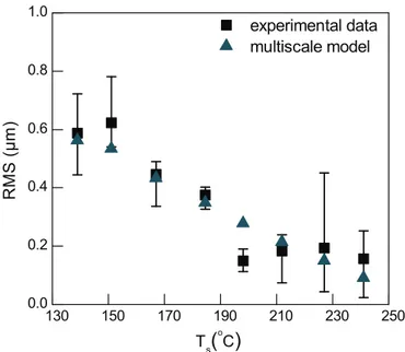
Fig. 4 presents the dependence of the RMS roughness on the temperature for both experimental measurements and computa-tional predictions. The RMS roughness of Al films deposited at the lower Ts(139 °C) is high (0.6 mm). RMS decreases with increasing
temperature and shows a minimum value of 0.15 mm at ca. 198 °C. Above this temperature RMS seems stable. It has been reported that above 200 °C the RMS slightly increases (Yun et al., 1998) but in our case such slight increase would lie within deviation intervals. Surface roughness is closely related to the change of the microstructure of the film. At a surface temperature below 150 °C, the Al film is not continuous and is composed of grains with a broad size distribution, resulting in high roughness. On the other hand, increasing Tsfrom
150 °C up to 227 °C results in smoother surface morphology with coalesced grains and decreasing open porosity with increasing
de-position temperature. The computational model accurately
reproduces the experimental data, since all the predicted RMS values, except for Ts¼198 °C, lie within the intervals of deviations. We as-sume that there is no physical reason of such an anomalous variation of the RMS at this particular Tsand its experimental value is
attrib-uted to an offset position.
Fig. 5shows the number of possible surface events (adsorption, migration, desorption) – directly correlated with R-quantities (Eq. (9)) as a function of Ts. It can be observed that in the investigated
temperature range, adsorption dominates the process, since the number of adsorption events is much higher than the corre-sponding number of migration and desorption events. Migration and desorption are enhanced as temperature increases and on the other hand, adsorption is restrained but the difference between them remains high. Despite the predominance of adsorption, the impact of the migration on the behavior of the RMS roughness is
Fig. 4. Evolution of RMS roughness with surface temperature, Ts. Experimental
data (squares) and multiscale calculations (triangles) are shown. Error bars corre-spond to deviations from minimum and maximum experimental values.
Fig. 5. The number of surface events, adsorption, migration, desorption, as a function of Ts. Adsorption, migration and desorption events are illustrated by black
squares, green triangles and brown circles, respectively. (For interpretation of the references to color in this figure legend, the reader is referred to the web version of this article.)
significant. In particular, it can be seen that as the number of migration events increases, the surface roughness decreases. This behavior is attributed to the fact that at low temperatures, the process is limited by the surface reaction and adsorption on the
surface (Aviziotis et al., 2015) which prevents diffusion from dis-seminating the atoms on the surface. On the other hand, at higher temperatures, diffusion dominates deposition yielding the more uniform distribution of the atoms on the surface; thus, the RMS roughness is reduced. Desorption may affect the RMS roughness in the sense that atoms that desorbed from the surface can re-adsorb in such lattice sites that roughness decreases. The main impact of desorption is on the deposition rate; at high temperatures, where it is observed that desorption events are increased, the Al de-position rate is reduced (Aviziotis et al., 2015;Xenidou et al., 2010). Fig. 6 shows the simulated surfaces (6a, 6b) and the corre-sponding experimentally obtained surfaces (6c, 6d) characterized by interferometry. The surfaces are processed at 151 °C (6a, 6c) and 227 °C (6b, 6d) and the surface heights are shown for each tem-perature. Although we are performing coarse-grained and not atomistic simulations at the nanoscale level, we observe that there are similarities among the simulated and experimental surfaces. Despite the fact that at low Ts the surface seems more
homo-geneous, the difference between the minimum and the maximum height is bigger and thus, the RMS is higher. On the other hand, at high Tsthe surface seems rougher at a large scale but the small
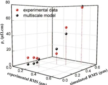
differences among the surface heights yield lower RMS values. Fig. 7presents the experimentally measured (red points) and the computed (black points) electrical resistivity. The former refer to the experimental RMS axis, while the latter to the multiscale model and to the simulated RMS axis. It can be seen that electrical resistivity increases with increasing roughness from 10μΩcm at
780 785 790 795 800 805
(a)
(b)
810 738 755 772 789 806 823 840(c)
(d)
Fig. 6. The morphology of the surface as predicted by the multiscale computational framework ((a), (b)) and as obtained by optical interferometry ((c), (d)) for 151 °C and 227 °C, respectively. Color scale is the same for both experimental and computational results which are at the same Ts. (For interpretation of the references to color in this
figure legend, the reader is referred to the web version of this article.)
o
Fig. 7. The measured (red spheres) and estimated with the multiscale model (black spheres) electrical resistivity of Al films as a function of the experimental and the simulated RMS roughness. (For interpretation of the references to color in this figure legend, the reader is referred to the web version of this article.)
RMS 0.15 mm to ca.80μΩcmat RMS 0.6 mm. These values and the observed evolution of the electrical resistivity are attributed to the increased scattering of the rough surfaces and to their significant contribution to the resistivity (Machlin, 2006). Moreover, grain boundary scattering may contribute a significant excess resistivity in polycrystalline Al films, since the grain boundaries do not scatter the conduction electrons (Francombe, 1988). Finally, O contamination within the film can lead to higher resistivity values. The dependence of the electrical resistivity on the RMS roughness has also been reported for other materials (Tang et al., 2003; Ti-malshina et al., 2015).
As previously mentioned, the extended FS model (Eq.(12)) is applied to estimate the electrical resistivity of Al films, while the thickness and the RMS roughness are provided by multiscale si-mulations. Concerning the specularity parameter, we assume a completely diffuse scattering from both the top and bottom sur-faces of the Al film, that is p¼0, a statement that holds true for surfaces with high roughness (Kanter, 1970). Finally, by fitting the estimated resistivity to the experimental data, we find α= 30, β= 5.6. The physical meaning of these parameters is not clear (Timalshina et al., 2015) and their fit may not be unique. However, we privilege the accuracy of the computed RMS values in order to have a reliable estimation of the electrical resistivity. The estima-tion of the electrical resistivity with the extended FS model ap-pears to be fairly good with regard to the corresponding experi-mental measurements and both datasets present the same trend. As roughness decreases, the discrepancy between experimental data and results provided by the multiscale model increases. This is attributed to the fact that in our estimations we do not in-corporate any information for grain boundaries or contamination. The accurate simulation of the surface microstructure and the control of RMS roughness through the variation of the operating conditions of the reactor, enable the control of the properties of the final film, such as the electrical resistivity. Assuming that surface roughness of crystalline materials often corresponds to the existence of grain boundaries, it may account for the increase in electrical resistivity through grain boundaries scattering of the electrons.
5. Conclusions
We experimentally and computationally investigate the RMS roughness and the electrical resistivity of Al films produced by a CVD process from DMEAA. In particular, for the two parameters we compare the experimentally measured values with those ob-tained by performing multiscale computations. Multiscale com-putations allow fetching from the surface of the growing film the information needed to compute the aforementioned properties.
The multiscale framework uses a 3D model of the reactor, based on the conservation equations, which computes the mass fractions of the precursor on the vicinity of the substrate. The outcome is fed to a nanoscale model, based on the kinetic Monte Carlo method, which simulates the evolution of the film and computes its surface roughness and its electrical resistivity. The chemical information for the decomposition of the precursor on the surface are incorporated in the sticking coefficient. For the latter, we implement a deposition temperature dependent func-tion by fitting experimental deposifunc-tion rates at various tempera-tures and at various positions on the susceptor.
The obtained results are compared with values of surface roughness of Al films processed in the same conditions. The ex-perimentally determined RMS roughness decreases with increas-ing the surface temperature, from 0.6 mm at 139 °C to 0.15 mm at 198 °C. The calculated RMS values lie within the deviations of experimental measurements. A very good agreement is obtained
between the experimental measurements and those calculated by the multiscale framework.
At low process temperature, adsorption dominates the process, while diffusion and migration events are few. Temperature in-crease results in the enhancement of migration and desorption which in turn results in the decrease of the surface roughness due to smoother distribution of atoms on the surface. Thus, despite the fact that adsorption is fitted to experiments, while desorption and migration are not, the impact of the two latter on the growth of the surface renders an unconstrained multiscale model.
The electrical resistivity of the films increases with increasing surface roughness from10μΩcmat RMS 0.15 mm to ca.80μΩcm
at RMS 0.6 mm, mainly due to the increased scattering caused by rough surfaces and to higher grain boundaries density which re-sults in the entrapment of electrons. The behavior of the electrical resistivity is quantitatively reproduced when the calculated re-sistivity is correlated with the simulated RMS of the films.
The presented multiscale computational framework can be implemented to perform similar analysis for other materials or for the simulation of similar surface phenomena taking into con-sideration the formation of more complex structures, such as di-mers or tridi-mers. The incorporation of chemical reactions at the nanoscale and the consideration of the crystallographic structure of the Al films (herefcc) within the nanoscale algorithm are under way. Thus, more species could be accounted for, and the simula-tion of more complex processes and surface features, such as is-land formation, grain boundaries and height-height correlation could be enabled. Regarding the calculation of the porosity evo-lution within the film, the SOS approximation should be replaced by triangular lattice models which, in contrast to the SOS models, can accommodate the formation of vacancies. In that case, alter-native multiscale methods such as coarse-graining with low-order macroscopic variables or equation-free methodologies will be implemented, to cope with the associated increased computa-tional effort.
Acknowledgments
This work was partially funded by the Institut Franais du Pet-role et des Energies Nouvelles (IFPEN), France through the contract #268821. IGA acknowledges the financial support provided by the National Scholarship Foundation of Greece (Grant number: #SpnD/11160/13
β
) (IKY-Siemens Program) and D. Same´lor (CIRI-MAT) for help with interferometry measurements. We are in-debted to the European Integrated Center for the Development of New Metallic Alloys and Compounds (C-MAC) for support.References
Albao, M.A., Putungan, D.B., Hsu, C.-H., Chuang, F.-C., 2013. Enhanced nucleation of Al islands on H-dosed Si(100)-2 " 1 surface: a combined density functional theory and kinetic Monte Carlo study. Surf. Sci. 617, 73–80.
Aviziotis, I.G., Duguet, T., Soussi, K., Kokkoris, G., Cheimarios, N., Vahlas, C., Bou-douvis, A.G., 2015. Investigation of the kinetics of the chemical vapor deposi-tion of aluminum from dimethylethylamine alane: experimentsand computa-tions. Phys. Status Solidi C 12, 923–930.
Barbato, A., Fiorucci, A., Rondanini, M., Cavallotti, C., 2007. Multiscale investigation of the influence of surface morphology on thin film CVD. Surf. Coat. Technol. 201, 8884–8887.
Battaile, C.C., Srolovitz, D.J., Butler, J.E., 1998. Atomic-scale simulations of chemical vapor deposition on flat and vicinal diamond substrates. J. Cryst. Growth 194, 353–368.
Battaile, C.C., Srolovitz, D.J., 2002. Kinetic monte carlo simulation of chemical vapor deposition. Annu. Rev. Mater. Res. 32, 297–319.
Bernd, A.B., 2004. Markov Chain, Monte Carlo Simulations and Their Statistical Analysis. World Scientific Publishing, Singapore.
Bormashenko, E., Stein, T., Whyman, G., Bormashenko, Y., Pogreb, R., 2006. Wetting properties of the multiscaled nanostructured polymer and metallic
superhydrophobic surfaces. Langmuir 22, 9982–9985.
Bravo, J., Zhai, L., Wu, Z., Cohen, R.E., Rubner, M.F., 2007. Transparent super-hydrophobic films based on silica nanoparticles. Langmuir 23, 7293–7298. Cavallotti, C., Barbato, A., Veneroni, A., 2004. A combined three-dimensional kinetic
Monte Carlo and quantum chemistry study of the CVD of Si on Si(1 0 0) sur-faces. J. Cryst. Growth 206, 371–380.
Cavallotti, C., Pantano, E., Veneroni, A., Masi, M., 2005. Multiscale simulation of silicon film growth. Cryst. Res. Technol. 40, 958–963.
Chaterjee, A., Vlachos, D.G., 2007. An overview of spatial microscopic and ac-celerated kinetic Monte Carlo methods. J. Comput.-Aided Mater. Des. 14, 253–308.
Cheimarios, N., Kokkoris, G., Boudouvis, A.G., 2010. Multiscale modeling in chemical vapor deposition processes: coupling reactor scale with feature scale compu-tations. Chem. Eng. Sci. 65, 5018–5028.
Cheimarios, N., Garnelis, S., Kokkoris, G., Boudouvis, A.G., 2011. Linking the oper-ating parameters of chemical vapor deposition reactors with film conformality and surface nano-morphology. J. Nanosci. Nanotechnol. 11, 8132–8137. Christofides, P.D., Armaou, A., Lou, Y., Varshney, A., 2008. Control and optimization
of multiscale process systems. In: Levine, W.S. (Ed.), Control Engineering Series, Birkhäuser, Boston.
Collins, S.D., Chaterjee, A., Vlachos, D.G., 2008. Coarse-grained kinetic Monte Carlo models: complex lattices, multicomponent systems, and homogenization at the stochastic level. J. Chem. Phys. 129 (184101), 1–15.
Crose, M., Kwon, J.S.-I., Nayhouse, M., Ni, D., Christofides, P.D., 2015. Multiscale modeling and operation of PECVD of thin film solar cells. Chem. Eng. Sci. 136, 50–61.
Deen, W.M., 1998. Analysis of Transport Phenomena. Oxford University Press, New York.
Delmas, M., Vahlas, C., 2007. Microstructure of metallorganic chemical vapor de-posited aluminum coatings on Ti6242 titanium alloy electrochemical/chemical deposition and etching. J. Electrochem. Soc. 154, D538–D542.
Evans, J.W., Thiel, P.A., Bartlet, M.C., 2006. Morphological evolution during epitaxial thin film growth: formation of 2D islands and 3D mounds. Surf. Sci. Rep. 61, 1–128.
Francombe, M.H., 1988. Physics of Thin Films: Advances in Research and Devel-opment. Academic Press, San Diego.
Giancoli, D.C., 2013. Physics: Principles with Applications, seventh ed. Pearson Prentice Hall, USA.
Gillespie, D.T., 1977. Exact stochastic simulation of coupled chemical reactions. J. Phys. Chem. 81, 2340–2361.
Gillespie, D.T., 2001. Approximate accelerated stochastic simulation of chemically reacting systems. J. Chem. Phys. 115, 1716–1733.
Gilmer, G.H., Bennema, P., 1972. Simulation of crystal growth with surface diffusion. J. Appl. Phys. 43, 1347–1360.
Gladfelter, W.L., 1993. Selective metalization by chemical vapor deposition. Chem. Mater. 5, 1372–1388.
Grujicic, M., Lai, S.G., 2000. Multi-length scale modeling of CVD of diamond part I: a combined reactor-scale/atomic-scale analysis. J. Mater. Chem. 35, 5359–5369. Hamasha, M.H., Alzoubi, K., Switzer III, J.C., Lu, S., Desu, S.B., Poliks, M., 2011. A study
on crack propagation and electrical resistance change of sputtered aluminum thin film on poly ethylene terephthalate substrate under stretching. Thin Solid Films 519, 7918–7924.
Han, J., Jensen, K.F., Senzaki, Y., Gladfelter, W.L., 1994. Pyrolytic laser assisted che-mical vapor deposition of Al from dimethylethylamine-alane:characterization and a new two-step writing process. Appl. Phys. Lett. 64, 425–427. Hersee, S.D., Ballingal, J.M., 1990. The operation of metalorganic bubblers at
re-duced pressure. J. Vac. Sci. Technol. A 8, 800–804.
Hu, G., Hu, X., Orkoulas, G., Christofides, P.D., 2010. Multiscale modeling and control of porous thin film growth. In: Levine, W.S. (Ed.), Control System Applications, second ed. CRC Press, USA, pp. 13-1–13-17.
Huang, H., Gilmer, G.H., de la Rubia, T.D., 1998. An atomistic simulator for thin film deposition in three dimensions. J. Appl. Phys. 80, 3636–3649.
Jang, T.W., Moon, W., Baek, J.T., Ahn, B.T., 1998. Effect of temperature and substrate on the growth behaviors of chemical vapor deposited al films with dimethy-lethylamine alane source. Thin Solid Films 333, 137–141.
Kadok, J., de Weerd, M.-C., Boulet, P., Gaudry, E., Grin, Y., Fournée, V., Ledieu, J., 2015. Al3AuIr: a new compound in the AlAuIr system. J. Inorg. Chem. 54, 7898–7905. Kanter, H., 1970. Slow-electron mean free paths in aluminum, silver, and gold. Phys.
Rev. B 1, 522–536.
Katsoulakis, M.A., Vlachos, D.G., 2003. Coarse-grained stochastic processes and kinetic Monte Carlo simulators for the diffusion of interacting particles. J. Chem. Phys. 129, 9412–9427.
Kim, H.J., Egashira, Y., Komiyama, H., 1991. Temperature dependence of the sticking probability and molecular size of the film growth species in an atmospheric chemical vapor deposition process to form AlN from AlCl3and NH3. Appl. Phys.
Lett. 59, 2521–2523.
Kim, B.-Y., Li, X., Rhee, S.-W., 1996. Microstructure and deposition rate of aluminum thin films from chemical vapor deposition with dimethylethylamine alane. Appl. Phys. Lett. 68, 3567–3569.
Lam, R., Vlachos, D.G., 2001. Multiscale model for epitaxial growth of films: growth mode transition. Phys. Rev. B 64 (035401), 1–10.
Latz, A., Brendel, L., Wolf, D.E., 2012. A three-dimensional self-learning kinetic Monte Carlo model: application to Ag (111). J. Phys.: Condens. Matter 24 (485005), 1–9.
Lee, H.M., Lee, H.B., Jung, D.S., Yun, J.-Y., Ko, S.H., Park, S.B., 2012. Solution processed aluminum paper for flexible electronics. Langmuir 28, 13127–13135.
Lee, H.M., Choi, S.-Y., Jung, A., 2013. Direct deposition of highly conductive alumi-num thin film on substrate by solution-dipping process. ACS Appl. Mater. In-terfaces 5, 4581–4585.
Lee, H.M., Seo, J.Y., Jung, A., Choi, S.-Y., Ko, S.H., Jo, J., Park, S.B., Park, D., 2014. Long-term sustainable aluminum precursor solution for highly conductive thin films on rigid and flexible substrates. ACS Appl. Mater. Interfaces 6, 15480–15487. Liu, S.J., Huang, H., Woo, C.H., 2002. Schwoebel-Ehrlich barrier: from two to three
dimensions. Appl. Phys. Lett. 80, 3295–3297.
Lou, Y., Christofides, P.D., 2003. Estimation and control of surface roughness in thin film growth using kinetic Monte-Carlo models. Chem. Eng. Sci. 58, 3115–3129. Machlin, E.S., 2006. Materials Science in Microelectronics II: The Effects of Structure
on Properties in Thin Films, second ed. Elsevier Ltd., UK.
Masi, M., Bertani, V., Cavallotti, C., Carrá, S., 2000. Towards a multiscale approach to the growth of silicon films by chemical vapor deposition. Mater. Chem. Phys. 66, 229–235.
Matsuda, A., Nomoto, K., Takeuchi, Y., Suzuki, A., Yuuki, A., Perrin, J., 1990. Tem-perature dependence of the sticking and loss probabilities of silyl radicals on hydrogenated amorphous silicon. Surf. Sci. 227, 50–56.
Nakajima, T., Nakatomi, M., Yamashita, K., 2003. Quantum chemical calculations on Al-CVD using DMEAA: surface reaction mechanism of AlH3on Al(111). Mol.
Phys. 101, 267–276.
Papanicolaou, N.I., Papathanakos, V.C., Papageorgiou, D.G., 2001. Self-diffusion on Al (100) and Al(111) surfaces by molecular-dynamics simulation. Physica B 296, 259–263.
Poling, B.E., Prausnitz, J.M., O'Connell, J.P., 2001. The Properties of Gases and Liquids, fifth ed McGraw-Hill, USA.
Raimondeau, S., Vlachos, D.G., 2000. Low-dimensional approximations of multi-scale epitaxial growth models for microstructure control of materials. J. Com-put. Phys. 160, 564–576.
Rapaport, C.D., 2004. The Art of Molecular Dynamics Simulation, second ed. Cam-bridge University Press, New York.
Raupp, G.B., Cale, T.S., 1989. Step coverage prediction in low-pressure chemical vapor deposition. Chem. Mater. 1, 207–214.
Rechendor, K., Hovgaard, M.B., Foss, M., Zhdanov, V.P., Besenbacher, F., 2006. En-hancement of protein adsorption indeced by surface roughness. Langmuir 22, 10885–10888.
Reese, J.S., Raimondeau, S., Vlachos, D.G., 2001. Monte Carlo algorithms for complex surface reaction mechanisms: efficiency and accuracy. J. Comput. Phys. 173, 302–321.
Rodgers, S.T., Jensen, K.F., 1998. Multiscale modeling of chemical vapor deposition. J. Appl. Phys. 83, 524–530.
Samélor, D., Sandowski, D., Senocq, F., Vahlas, C., 2010. Device for measuring the electrical properties of thin films at high temperature. Appl. Number FR1 0, 51074.
Seah, M., de Chiffre, L., 2006. Surface and interface characterization. In: Czichos, H., Saito, T., Smith, L. (Eds.), Springer Handbook of Materials Measurements Methods. Springer ScienceþBusiness Media, Würzburg, pp. 229–272. Simmonds, M.G., Taupin, I., Gladfelter, W.L., 1994. Selective area chemical vapor
deposition of aluminum using dimethylethylamine alane. Chem. Mater. 6, 935–942.
Srolovitz, D.J., Dandy, D.S., Butler, J.E., Battaile, C.C., Paritosh, 1997. The integrated multiscale modeling of diamond chemical vapor deposition. JOM 4 (9), 42–47. Stumpf, R., Scheffler, M., 1996. Ab initio calculations of energies and self-diffusion on flat and stepped surfaces of Al and their implications on crystal growth. Phys. Rev. B 53, 4958–4973.
Tan, C.M., Roy, A., 2007. Electromigration in ULSI interconnects. Mater. Sci. Eng. R Rep. 58, 1–75.
Tang, W., Xu, K., Wang, P., Li, X., 2003. Surface roughness and resistivity of Au film on Si-(111) substrate. Micro. Eng. 66, 445–450.
Timalshina, Y.P., Horning, A., Spivey, R.F., Lewis, K.M., Kuan, S., Wang, G.-C., Lu, T.-M., 2015. Effects of nanoscale surface roughness on the resistivity of ultrathin epitaxial copper films. Nanotechnology 26 (075704), 1–10.
Thomann, A.-L., Vahlas, C., Aloui, L., Samélor, D., Caillard, A., Shaharil, N., Blanc, R., Millon, E., 2011. Conformity of aluminum thin films deposited onto micro-patterned silicon wafers by pulsed laser deposition, magnetron sputtering, and CVD. Chem. Vap. Depos. 17, 366–374.
Tsalikis, D.G., Baig, C., Mavrantzas, V.G., Amanatides, E., Mataras, D., 2013. hybrid kinetic Monte Carlo method for simulating silicon films grown by plasma-en-hanced chemical vapor deposition. J. Chem. Phys. 139 (204706), 1–14. Vahlas, C., Blanquet, E., 1998. Thermochemistry of Silicon LPCVD Revisited with
Kinetic Data. In: Branz, H.M., Hack, M., Schropp, R., Shimizu, I., Wagner, S. (Eds.), Amorphous and Microcrystalline Silicon Technology. Cambridge University Press, pp. 951–956.
Vahlas, C., Ortiz, P., Oquab, D., 2001. Toward the improvement of the microstructure of chemical vapor deposited aluminum on silicon carbide. J. Electrochem. Soc. 148, C583–C589.
Venkateswaran, N., Karpov, I., Gladfelter, W., Franciosi, A., 1996. Morphology and growth mode of Al films deposited by chemical vapor deposition from di-methylethylamine alane on GaAs(001)2 " 4 surfaces. J. Vac. Sci. Technol. A 14, 1949–1956.
Vlachos, D.G., 2008. Temporal coarse-graining of microscopic-lattice kinetic Monte Carlo simulations viaτleaping. Phys. Rev. E 78 (046713), 1–7.
Xenidou, T.C., Boudouvis, A.G., Markatos, N.C., Samélor, D., Senocq, F., Prud'homme, N., Vahlas, C., 2007. An experimental and computational analysis of a MOCVD process for the growth of Al films using DMEAA. Surf. Coat. Technol. 201, 8868–8872.
Xenidou, T.C., Prud'homme, N., Vahlas, C., Markatos, N.C., Boudouvis, A.G., 2010. Reaction and transport interplay in Al MOCVD investigated through experi-ments and computational fluid dynamic analysis. J. Electrochem. Soc. 157, D633–D641.
Yanguas-Gil, A., Yang, Y., Kumar, N., Abelson, J.R., 2009. Highly conformal film growth by chemical vapor deposition. I. A conformal zone diagram based on kinetics. J. Vac. Sci. Technol. A 27, 1235–1243.
Yun, J.-H., Kim, B.-Y., Rhee, S.-W., 1998. Metal-organic chemical vapor deposition of aluminum from dimethylethylamine alane. Thin Solid Films 312, 259–264. Yun, J.-H., Rhee, S.-W., 1998. Effect of carrier gas on metal-organic chemical vapour
deposition of aluminium from dimethylethylamine alane. J. Mater. Sci.: Mater.
Electron. 9, 1–4.
Zhang, Y., Hu, G., Orkoulas, G., Christofides, P.D., 2010. Controller and estimator design for regulation of film thickness, surface roughness, and porosity in a multiscale thin film growth process. Ind. Eng. Chem. Res. 49, 7795–7806. Zhdanov, V.P., Rechendorff, K., Hovgaard, M.B., Besenbacher, F., 2008. Deposition at
glancing angle, surface roughness, and protein adsorption: Monte Carlo simu-lations. J. Phys. Chem. B 112, 7267–7272.
Zorn, D.D., Albao, M.A., Evans, J.W., Gordon, M.S., 2009. Binding and diffusion of Al adatoms and dimers on the Si(100)-2 " 1 reconstructed surface: a hybrid QM/ MM embedded cluster study. J. Phys. Chem. C 113, 7277–7289.