Pépite | Anisotropie de la conductivité thermique artificiellement induite dans des membranes phononiques en silicium
153
0
0
Texte intégral
(2) Thèse de Stanislav Didenko, Université de Lille, 2019. Acknowledgements This PhD scientific project had been conducted in the Silicon Microelectronics Group at Higher Institute for Electronics and Digital Training (ISEN), Institute of Electronics, Microelectronics and Nanotechnology (IEMN) and financially supported by UPTEG (unconventional principles of thermoelectric generation) project (Grant №33κ17λ ). I am grateful to many people who helped me throughout this thesis project. I would like to address deep acknowledgments to: The director of my thesis Prof. Emmanuel Dubois: for giving me the chance to do the PhD project in his research group, for his supervision, support, valuable advices and inspiring motivation. Co-director of my thesis Prof. Thomas Skotnicki: for being my scientific supervisor; for the fruitful discussions. My supervisor Dr. Jean-François Robillard: for guiding me in my research and being open for the discussions whenever it was needed; for his reasonable advices regarding many aspects of my work; for being friendly and supportive; for his sense of humor and the optimism; his patience and his faith in his student. Thank you to my girlfriend Anna Kozina, for all her love and support, and teaching me Python. All the colleagues from my scientific group: for their openness to discussions and exchange of the research experience. Thus, many thanks are addressed to Valeria Lacatena, Maciej Haras, Valentina Giorgis, Justine Philippe, Quentin Hivin, Thierno Bah, Di Zhou, Antoine Frappé, Tianqi Zhu, Arun Bahskar and Jun Yin. Special thanks are addressed to Valeria Lacatena and Maciej Haras, whose fabrication projects became the foundation for my work. Pierre-Olivier Chapuis (CETHIL, Lyon): for discussions and the theoretical support of my work in the domain of Monte Carlo simulation, his efforts and the time spent organizing the collaboration between our lab and INSA-CETHIL colleagues. Our colleagues from INSA-Lyon, CETHIL and INL: Jean-Marie Bluet, A. Massoud and R. Orobtchouk, who performed crucial to my work RCWA analysis. IEMN engineers Marc Derwitte, Yves Deblock, François Vaurette, Christiane Legrand, Laurence Morgenroth, Guillaume Cochez, Pascal Tilmant, Dimitri Yareka, Garrett Curley, Christophe Boyaval, Isabelle Roche-Jeune, etc., who shared their knowledge and provided me with the technical support, without which this work would not be possible. Jean-Michel Droulez: for his technical support and programming advices. Maya Marinova (Lille1, Unité Matériaux et Transformations) and David Troadec (IEMN): for their important collaboration, which allowed to obtain fascinating TEM scans. Dominique Vignaud: for letting me work in his RT laboratory; for a great help provided during the work on set-up upgrade; for the technical and theoretical support. Florence Alberti: for her great organization and management skills, which helped me to feel a lot more comfortable in France and during the conference missions. Our colleagues from Université de Lorraine and INSA-Lyon: Maxime Verdier, David Lacroix and Konstantinos Termentzidis, who provided me with deep fundamental insight into the picture of thermal transport in phononic membranes at the presence of the amorphous oxide. Evelyne Martin (IEMN) and Stéphane Monfray (STMicroelectronics): for interesting suggestions and helpful discussions. 2 © 2019 Tous droits réservés.. lilliad.univ-lille.fr.
(3) Thèse de Stanislav Didenko, Université de Lille, 2019. List of the added corrections: Double spaces were deleted p.110 - Remark was added, regarding the question about the bulk Si and thin-film Si k(T) dependence. p.127 - Remark was added, regarding the question about k-tensors difference for experiment and simulation p.119 - attention remark was added in Figure 4.4 concerning 100nm pitch membranes difference among isotropic and anisotropic series. p.87 - the phrase "utilizing its Raman scattering properties" is added, implying that, indeed, the Laser is not a Thermometer in the direct sense. Figure 3.12, "Wavelength" was changed to the "Raman Shift" on the plot. p.102 - Sentence "Non-radians units are in m, in formulas below" was added. p.102 - One sentence added into the description of the "knife" method, to make it more detailed. p.115 - Words "comparing to the bulk value, or 5-fold reduction comparing to the pristine 44nm-thick membrane" were added to make a clear comparison. p.113 - Figure 4.1 Plot (c): the missing curve for Maxwell-Garnett formula was added. p.140 - List of the used abbreviations in alphabetic order was added into Appendix. 76th item of Literature was modified. Around 30 spelling and typo corrections were added around the manuscript.. 3 © 2019 Tous droits réservés.. lilliad.univ-lille.fr.
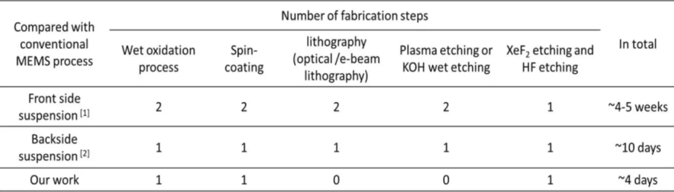
(4) Thèse de Stanislav Didenko, Université de Lille, 2019. Table of content ACKNOWLEDGEMENTS.........................................................................................................2 TABLE OF CONTENT ..............................................................................................................4 INTRODUCTION ......................................................................................................................6 CHAPTER 1. THERMAL TRANSPORT IN NANOSTRUCTURED MEMBRANES ........8. 1.1. Heat transport in Bulk Si ...................................................................................................................9 1.1.1 Dispersion curve and phononic band structure......................................................................... 9 1.1.2 Towards dominant phonon calculation .................................................................................. 11 1.1.3 Boltzmann transport equation, Fourier's law and scattering processes ................................... 13. 1.2. Literature review of thermal conductivity modulation experiments ............................................... 14 1.2.1 Coherent and incoherent effects in different transport regimes ............................................. 14 1.2.2 Diffusive and ballistic transport in thin-film membranes as a function of T ............................. 16 1.2.3 Thermal conductivity of phononic membranes at a room temperature .................................. 17 1.2.4 The role of the native oxide and the roughness ...................................................................... 19 1.2.5 Free-standing beam-like phononic membranes fabrication at Silicon Microelectronics group . 21. 1.3. Conclusions ..................................................................................................................................... 22. CHAPTER 2 DEVICES. DESIGN AND FABRICATION OF THE EXPERIMENTAL PHM 24. 2.1. Membrane geometry and the alignment of phononic patterns ...................................................... 25 2.1.1 Directionality of the measurements. ...................................................................................... 25 2.1.2 Heat current and measurement techniques. .......................................................................... 26 2.1.3 Membranes shape ................................................................................................................. 28 2.1.4 Design of phononic anisotropic patterns ................................................................................ 29. 2.2. Overview of the fabrication methods and experimental devices design ......................................... 32 2.2.1 Clean-room fabrication procedures........................................................................................ 32 2.2.2 Nanopatterning ..................................................................................................................... 37 2.2.3 Membrane fabrication techniques ......................................................................................... 40. 2.3. Overview of the fabrication process ............................................................................................... 43 2.3.1 The wafer preparation (cutting and layout). ........................................................................... 44 2.3.2 Alignment markers ................................................................................................................ 47 2.3.3 New method for holes quality assessment with the tilted lattices' cleaving ............................ 49 2.3.4 Nanopatterns engineering. .................................................................................................... 52 2.3.5 Cavities formation ................................................................................................................. 64 2.3.6 Oxidation............................................................................................................................... 66 2.3.7 Pre-etching opening of cavities .............................................................................................. 69 2.3.8 Die singulation ....................................................................................................................... 70. 4 © 2019 Tous droits réservés.. lilliad.univ-lille.fr.
(5) Thèse de Stanislav Didenko, Université de Lille, 2019. 2.3.9 2.4. Membranes release ............................................................................................................... 71. Conclusions ..................................................................................................................................... 75. CHAPTER 3. CHARACTERISATION METHODS........................................................... 78. 3.1. Post-fabrication structural characterisation .................................................................................... 78 3.1.1 SEM observation of the fabricated membrane ....................................................................... 78 3.1.2 Membrane width ................................................................................................................... 79 3.1.3 Thickness estimation ............................................................................................................. 79 3.1.4 Holes patterns characteristics and experimental goals ........................................................... 81 3.1.5 TEM study of the surface roughness and oxidation................................................................. 83. 3.2. Micro-Raman Thermometry............................................................................................................ 87 3.2.1 Experiment general overview................................................................................................. 87 3.2.2 Set-up.................................................................................................................................... 89 3.2.3 Temperature of the heating spot determined by µRT ............................................................. 91 3.2.4 Estimating the absorption ...................................................................................................... 93 3.2.5 Modelling the thermal conductivity ....................................................................................... 95 3.2.6 Absorption estimation for new phononic membranes ............................................................ 98 3.2.7 Attempt to eliminate photonic effects ................................................................................. 100 3.2.8 Determination of the laser beam size ................................................................................... 101 3.2.9 Experiment upgrade ............................................................................................................ 104 3.2.10 New measurement approach ............................................................................................... 106. 3.3. Conclusions ................................................................................................................................... 110. CHAPTER 4. RESULTS AND DISCUSSION ..................................................................112. 4.1. Experimental results ..................................................................................................................... 112 4.1.1 PhMs with isotropic lattices ................................................................................................. 112 4.1.2 PhMs with anisotropic lattices ............................................................................................. 114 4.1.3 Unexpected thermal conductivity reduction......................................................................... 118 4.1.4 Thermal conductivity vs. porosity and the neck size ............................................................. 122. 4.2. Possible implementations of the discovered thermal effects ........................................................ 125 4.2.1 Reduction of local T around fragile IC components ............................................................... 125 4.2.2 Anisotropic patterning as an alternative to IC modules' shifting............................................ 128. 4.3. Conclusions ................................................................................................................................... 131. GENERAL CONCLUSIONS AND PERSPECTIVES ...........................................................134 APPENDIX............................................................................................................................138 BIBLIOGRAPHY ..................................................................................................................143. 5 © 2019 Tous droits réservés.. lilliad.univ-lille.fr.
(6) Thèse de Stanislav Didenko, Université de Lille, 2019. Introduction As the Moore's law is pushed to its saturation limit, the thermal management becomes the crucial bottleneck of the Integrated Circuits (IC) design. The larger die sizes and more densely-packed IC elements make it harder to sink the heat away from the sensitive areas. The novel 3D integration approach makes IC structures that are even more complex from the thermal point of view, with many interfaces, which thermal contact resistance may be high. The averaged heat power density dissipated in a typical IC is of the order of 100W/cm². Usual thermal strategies treat the overheating issues partially at the expense of the computation speed (additional propagation delay) or the surface footprint, and require sophisticated thermal models. There is a lack of a complementary strategy, based on material properties rather than design and modelling. The directional redistribution of the in-plane heat flow in the silicon layer may become a promising tool in the toolbox of IC thermal management. This approach can be based on the artificially induced anisotropy of the inplane effective thermal conductivity in Si thin films or IC layers. In this work, the design, fabrication and characterisation development efforts were directed to resolve the question of the feasibility of such thermal transport anisotropy. Besides being perspective in the thermal management applications, the directional heat guiding can become an important functional element of the thermoelectric generators (TEG) based on thin film silicon membranes, which are CMOS-compatible and possesses low (high) thermal (electronic) conductivity. Induced anisotropic heat guiding in Si thin films can be achieved via the nanostructuring, e.g. an introduction of the lattice of nanoholes with the rectangular unit cell. The key role is played by the mechanisms of phonon scattering, that allows for artificial modulation of Si thermal transport properties in coherent (wave-like) or incoherent (particle-like) manner. The first chapter of this manuscript is devoted to the review of the fundamental theoretical aspects of the thermal transport in the bulk Si (band structure, Bose-Einstein distribution, dominant wavelength of phononic energy spectrum, Boltzmann transport equation, phonons scattering processes as a function of temperature). Then referring to the bulk properties, the most recent experimental and theoretical studies of the heat transport in low-dimensional and nanostructured silicon are discussed, addressing the question of dominant thermal conductivity reduction mechanisms at room and low temperatures. Phononic nanostructuring can be realized by the means of state-of-the-art patterning technologies such as e-beam nanolithography (EBL) combined with the plasma etching. Among various Si nanostructures (suspended phononic nanomeshes and nanowires), 2D Si phononic membranes (PhMs) attract the interest since they exhibit ≈20-fold reduction of thermal conductivity as compared to the bulk and at the same time their geometry is closer to IC Si thin layers. This work is the continuation of ERC UPTEG project, during the first stage of which design and fabrication strategies for the beam-like suspended Si membranes were developed by Valeria Lacatena and Maciej Haras. The second chapter describes, how using existing fabrication methodology the new approach, which addresses the question of artificially-induced anisotropy of thermal conductivity in 2D phononic membranes, was elaborated. The thermal transport experiment based on the vacuum micro Raman 6 © 2019 Tous droits réservés.. lilliad.univ-lille.fr.
(7) Thèse de Stanislav Didenko, Université de Lille, 2019. Thermometry (µRT) measurements of free-standing beam-like (FSBL) membranes with anisotropic lattices of nanoholes was proposed. FSBL topology allows for direct measurements of effective thermal conductivity eigenvalues in principle orientations of 2D anisotropic phononic lattice. The vacuum-based µRT implies the non-invasiveness and the elimination of both convection losses and interface resistance due to the absence of the metallic probes. Details concerning the improvement of the processing steps, that were only partially successful in previous methodology work or had a limited functionality, are given: obtaining a decent quality of the nanoholes etching; implementation of a new test-probe method allowing the fast assessment of the profiles of the etched nanoholes; finding optimal EBL writing method for anisotropic phononic patterns; etc. The measurement of thermal properties of fabricated PhMs and interpretation of the experimental results require the knowledge of geometrical (width, thickness) and structural (holes diameter, roughness, surface oxide thickness) characteristics. Chapter 3 describes how those characteristics were estimated, using scanning and transmission electron microscopy (SEM and TEM), electron dispersive x-ray spectroscopy (EDX), ellipsometry, laser interferometry, optical microscopy and statistical image analysis. The issues connected with the measurement methodology and data analysis are discussed: laser beam profile estimations, the installation of continuous variable filter and reference Si photodiode detector (which allowed to conduct the power-variation RT experiment with a bigger set of measurement points). By the combined use of RT, Rigorous Coupled Wave Analysis (RCWA), performed by colleagues from Institut des Nanosciences de Lyon (INL) and Centre d'Energétique et de Thermique de Lyon (CETHIL), and Finite Element Modelling (FEM) it was possible to measure the thermal gradient and membranes' effective thermal conductivity . Chapter 4 is devoted to the obtained results and their possible application. Based on the new experimental methodology, a graphical isotropic/anisotropic visualisation of the heat flow was proposed. The ratio of effective principal components was found: 2.2 for the pitch ratio of anisotropic lattice of holes (r) equal to 2.5 and 1.9 for r=2. Besides, 25-fold reduction of the thermal conductivity was observed for r=2.5 pattern: kyy= 6±0.6Wm-1K-1. This experiment confirms the possibility to induce artificially high anisotropy of in Si PhMs almost not changing the filling fraction (ff) and the diameter of the holes. At last, parameterized FEM Comsol model had been used for the purpose of demonstrating the possible implementation of induced anisotropic effects in the area of IC thermalmanagement.. 7 © 2019 Tous droits réservés.. lilliad.univ-lille.fr.
(8) Thèse de Stanislav Didenko, Université de Lille, 2019. Chapter 1 Thermal transport membranes. in. nanostructured. The recent developments in micro- and nanofabrication have made possible the synthesis of semiconductor materials with nanoscale modifications. New classes of materials with reduced dimensionality have emerged: quantum dots, nanowires, thin films (including Si phononic membranes). Such materials exhibit new properties in both electronic and phononic heat transport. The characteristic length of these functional materials is comparable to or shorter than the mean free path or wavelength of the heat carriers, which include molecules, photons, electrons, phonons, and magnons1. Accurate theoretical and experimental treatment is required for this class of material. This chapter reviews some fundamental phononic theoretical aspects of the bulk Si: dispersion relation, band structure, statistical treatment of phonons with Bose-Einstein distribution, Wien's displacement law and the dominant wavelength of phononic energy spectrum, kinetic model based on Boltzmann transport equation, Matthiessen’s rule and phonons scattering processes as a function of temperature. Then the most recent experimental and theoretical studies of the heat transport in lowdimensional and nanostructured silicon are discussed, addressing the question of dominant thermal conductivity reduction mechanisms at a room and low temperatures: incoherent and coherent effects.. 8 © 2019 Tous droits réservés.. lilliad.univ-lille.fr.
(9) Thèse de Stanislav Didenko, Université de Lille, 2019. 1.1 Heat transport in Bulk Si The crystal materials comprise the periodical lattice of atoms. At non zero temperature atoms are displaced from their equilibrium positions, i.e. from the minimum potential energy of their interaction forces. Displaced atoms vibrate around the equilibrium position due to unbalanced forces. Collective atomic vibration motions can be viewed as a series of harmonic and anharmonic waves, that can propagate the energy from the hot spots of the material to the cold ones. The energy levels of vibrational waves are quantized. A single quanta of the lattice vibration is called phonon. Phonons can be viewed as both waves and particles. In this section the main theoretical models that account for wave-like and particle-like aspects of phonons, are reviewed. 1.1.1 Dispersion curve and phononic band structure Let's consider the simplest case of atomic vibration: one-dimensional chain of atoms which move only along x axis (longitudinal motion). Silicon crystal has a two-atomic basis2, it means that its primitive cell in each point contains two atoms. Therefore, in our simple model the chain consists of atoms of two kinds. In a real crystal each of the two atoms experiences different interatomic force. In order to simplify the problem, we take an assumption that difference of interatomic forces can be viewed as difference of atomic masses or effective masses (M1 and M2 on the figure below). In this case the chain comprises two kinds of atoms connected with the springs of the same constant.. Figure 1.1. One-dimensional chain of atoms, with masses M1 and M2. Constant a is the interatomic distance.. Finally, taking the assumption that vibrations are harmonic (no damping forces), we can describe the motion of the atoms with the following equations:. M1. d 2un C (2un un 1 un 1 ) dt 2. d 2un 1 M2 C (2un 1 un 2 un ) dt 2. (1). where C is the spring constant, ui is the displacement of an atom from its equilibrium position.. 9 © 2019 Tous droits réservés.. lilliad.univ-lille.fr.
(10) Thèse de Stanislav Didenko, Université de Lille, 2019. The solutions are expected to be in a form:. un A1e i ( qnat ) un1 A2 ei ( q( n1) a t ). (2). where A is the amplitude of the displacement, q is the wave vector, a is the interatomic distance, and ω is the frequency. Substituting (2) into (1), and solving the system of two linear equations 3, one can derive the dispersion relation:. 2 C(. 1 1 1 1 2 4 sin 2 qa )C ( ) M1 M 2 M1 M 2 M 1M 2. (3). The two curves for respective sign of the dispersion equation are plotted below. The curve, which starts at q=0 and ω=0, is called "acoustic branch", it corresponds to elastic waves of sound. Another curve is called "optical branch". The largest contrast between the two branches can be seen if we compare the lattice vibration at q = 0 (infinite wavelength). According to the equations, the acoustic branch has A1 = A2 if q=0. It means that the amplitude and the phase of both atoms is the same, in other words, the whole chain oscillates as a rigid body.. Figure 1.2. Optical and acoustic branches of one-dimensional chain of atoms.. One can show that atoms in the optical branch have antiphase oscillations, thus the centre of mass of the chain does not change. Optical oscillations occur at the infrared frequency. This property is of particular importance in this work, because the experiment is based on the Raman (light) scattering form the optical phononic modes (see Paragraph 3.2.3). In the next paragraph it will be shown that the group velocity of phonon wavepacket, which is the derivative of the dispersion curve υg=dω/dq, is proportional to thermal conductivity. Conventionally the group velocity is calculated only from the dispersion of acoustic phonons, for the reason that their contribution to is the largest (derivative of the. 10 © 2019 Tous droits réservés.. lilliad.univ-lille.fr.
(11) Thèse de Stanislav Didenko, Université de Lille, 2019. optical branch is much lower than the acoustic one). Acoustic phonons are often called thermal.. Figure 1.3. Phonon dispersion curves4 for the [100], [110], and [111] directions in silicon based on neutron scattering data. The two transverse phonon branches are degenerate in each of the directions.. In the three-dimensional crystals the atomic vibrations also split into the optical and acoustic branches. The figure above demonstrates Si phononic band structure for three high symmetry crystal directions. In modes' abbreviations (LA, TA, LO, TO), the first letter indicates the polarisation of atomic displacement (transverse or longitudinal) and the second indicates the branch (optical or acoustic). As for 1D chain example, for 3D Si crystal we observe the same situation for υg, which is high for LA and TA modes. 1.1.2 Towards dominant phonon calculation According to Debye model, atomic oscillations are quantized2. Because any crystal has a finite size, there is a finite number of possible energy levels for oscillations. The phonon is a quantum of particular vibration energy (ε=hω/2π). There are two main assumptions which allow to treat phonons statistically. The first is that any number of phonons can occupy the same energy state. The second assumption is that there are many more energy levels than phonon particles. If gi is a number of energy levels in a small ith energy interval and ni is the number of phonons that occupy this interval, then the total number of all possible arrangements of the energy states in all intervals5:. i. (ni g i )! ni ! g i !. (4). Maximizing Ω with Lagrange multiplier method, putting the constraint of the constant energy at 0K, and substituting Lagrange multiplier with the measure of entropy (-1/KBT, where KB is Boltzmann constant), one can derive the distribution of phonon energy with respect to the temperature. 11 © 2019 Tous droits réservés.. lilliad.univ-lille.fr.
(12) Thèse de Stanislav Didenko, Université de Lille, 2019. n( ) g ( ). 1. (5). . e. K BT. 1. The last expression is called Bose-Einstein distribution. In order to estimate the total energy U, the density of states function g(ε) is needed. One can show that for 3D crystal, accounting for 3 modes of polarisations, g(ε) is expressed as:. g ( ) 3. V 2 2 2v 2. where V is the volume, v=ω/q is the velocity of a phonon .. (6). Expressing everything in terms of angular frequency, and integrating over ħωn(ω)dω, we obtain:. U. 3Vh 4 3v 3. . D. 0. 3d e h / 2K BT 1. Where ωD is the Debye cut-off frequency, which is related to the fact that the wavelength cannot be shorter than interatomic distance. v=ω/q is the velocity of a phonon.. (7). At a low temperature U is proportional to T4, which is the same as for Stephan-Boltzman law of photon radiation6. This is the reason why heat transport by phonons is often called phonon radiation. From the mentioned proportionality of U and T 4 it follows that the expression under the integral is an analogue to Plank distribution for phonons. Hence similarly to photonic distribution for black body radiation, we can differentiate phononic Plank distribution to obtain Wien's displacement law for phonons: ħωdom =KBT, where ωdom is the dominant frequency for phonons. Figure 1.47 demonstrates the distribution of phonons with respect to the wavelength and the T, where the dominant wavelengths dom correspond to the maximum of the curves. dom is of the order of 1nm at a room temperature (RT) and 100nm at 1K.. Figure 1.4. Phonon spectral density7 as a function of the wavelength for different equilibrium temperatures of a black body.. 12 © 2019 Tous droits réservés.. lilliad.univ-lille.fr.
(13) Thèse de Stanislav Didenko, Université de Lille, 2019. 1.1.3 Boltzmann transport equation, Fourier's law and scattering processes Boltzmann transport equation (BTE) treats phonons as particles, which are described by the nonequilibrium distribution function u(r, k, t), that can be interpreted as the probability of finding the particle at position r with wavevector k at a time t. In the case of a collision at a time t+dt the differential of the distribution function is: = ( +. , +. , +. )− ( , , )=. (. ). (8). Under the assumption that no external force exerts on the system, and applying the single relaxation time approximation, one can derive the equation describing particle diffusion : +. �. ∇. =−. − �. 0. (9). In this expression u0 is the equilibrium distribution, vg is the velocity of heat carriers (or group velocity in the wavepacket picture), τ is the relaxation time. Solving for heat flux current qy [J/( m2 s)] in particular direction, one obtains the Fourier law: 1 ( ) � ( ) �( ) 3 0 where Cp(ω) [J s / (m3K)] is the volumetric modewise heat capacity. Λ is the mean free path of the phonon. ωmax is the maximum frequency (Debye frequency) =−. (10). Fourier law relates the temperature gradient to the heat current via thermal conductivity. Simplifying (9) for the specific heat, averaged values of the group velocity and the mean free path one can obtain: 1 (11) = −� ; � = � 3 � As we can see, the thermal conductivity depends on the knowledge of dispersion curves (group velocity), specific heat, and the mean free path (or relaxation time). For the bulk material the mean free path can be expressed according to Matthiessen’s rule, which combines boundary (B), impurity (I) and Umklapp (U) scattering contributions: (12). −1 �−1 = �−1 + �−1 � +� The boundary and impurity scattering processes are dominant extrinsic scattering mechanisms8. The first is attributed to the scattering of the phonons on the surface of the material. Hence, the surface roughness plays a crucial role because the dominant phonon wavelength at RT is of the order of 1nm (as was shown in the previous paragraph), and this value is the same for the roughness on the typical Si surfaces. In low-dimensional nanostructured materials, the boundary scattering contribution to the mean free path is usually a fitting parameter9. Impurity scattering is proportional to the dopant concentration and can be found in literature. The last term in Matthiessen’s rule accounts for the dominant intrinsic scattering process called Umklapp scattering. It is an anharmonic quadratic (four. 13 © 2019 Tous droits réservés.. lilliad.univ-lille.fr.
(14) Thèse de Stanislav Didenko, Université de Lille, 2019. phonons) or cubic (three phonons) process (three/two phonons can collide forming the third/forth one). In the case when the wave vector of created phonon falls outside the first Brillion zone, the total phonon momentum changes according to the addition of the reciprocal lattice vector G. This creates a flux in the opposite direction to heat propagation. The Umklapp processes become more dominant with the temperature. At a low T, the boundary scattering dominates because the MFP is longer than the sample size. The figure below summarizes the dominant scattering mechanisms' contribution into the bulk Si thermal conductivity at different T. Impurity scattering. Boundary scattering κ~T3. Umklapp scattering κ~T-1 (T-1.5). Figure 1.5. Thermal conductivity of Si as a function of T measured with radial heat-flow method10 and remarks for dominant scattering mechanisms' contributions8.. 1.2 Literature review of thermal conductivity modulation experiments In this chapter, some recent experimental and simulation studies for low-dimensional Si materials will be reviewed. As was shown in the previous chapter, phononic properties, such as the mean free path and the dominant wavelength, are both temperature dependant. Now we are interested in the question, how do the phononic properties regulate the thermal conductivity in nanostructured Si systems. 1.2.1 Coherent and incoherent effects in different transport regimes Conventionally there are two types of phononic effects that can dominate in the reduction of thermal conductivity: incoherent and coherent. The first type of effects is connected with the particle-like picture of phonons, which can experience boundary and impurities scattering. Kinetic BTE model is used to describe incoherent phonons. To the contrary, coherent phonons are viewed as the waves, which can interfere or Bragg scatter. This implies that the reduction of thermal conductivity for coherent phononic transport can be initiated by the reduction of the group velocity (phononic band gap modification) or destructive interference. 14 © 2019 Tous droits réservés.. lilliad.univ-lille.fr.
(15) Thèse de Stanislav Didenko, Université de Lille, 2019. Depending on the T, the size of the sample and the roughness of the surface, the contribution from these two effects into thermal transport can change. Different transport regimes are distinguished, each of them is described with specific model. In the work of O. Bourgeois et al7 a good summary of these regimes is given (Figure below).. Figure 1.6. Classification of the different regimes7 of phonon transport in nanoscaled systems at low enough temperature, typically below 30K for silicon. L is the sample length, Λ ph is the inelastic phonon mean free path, and dom is the dominant phonon wavelength. Kcas is the thermal conductance in Casimir regime. Concerning the Landauer limit, the parameter T denotes the transmission coefficient between a nanowire and its heat reservoir. Other important lengths are explained in the text.. The diffusive regime is described by the kinetic model, and is mostly attributed to the bulk material. Incoherent effects are dominant. Thin-film membranes at a RT also can be attributed to this regime if both MFP and dom are smaller than the length of the sample. Decreasing the T and/or the length of the sample, we approach the Casimir regime, when MFP for the bulk is bigger than the reduced MFP inside the sample. Even though this limit is reached7 at a low enough T, only the boundary scattering mechanism, linked to the surface roughness, dominates. In the Ziman regime the T drops even further, hence the dom becomes larger than the roughness amplitude7 and specular reflections of phonons on the surface cannot be neglected. p in the Ziman model is the probability parameter of a phonon to be specularly reflected on the surface, which depends on the wavelength of a phonon and the roughness. Basically, the same formula from the Casimir model conductance can be applied for Ziman and ballistic regimes, if the Λcas is replaced by an effective MFP Λph from the Ziman formula. Specularity parameter p=1 means that all the phonons scatter coherently and ballistic transport limit is reached (elastic MFP is diverging to infinite). The ballistic regime has to be described with Landauer formalism11 where the transport is determined via the transmission coefficient with the assumption of zero temperature gradient within the sample. According to Fourier's law, for zero T gradient the thermal conductivity cannot be prescribed. In the ballistic regime, the heat transport can be explained only in terms of the thermal conductance.. 15 © 2019 Tous droits réservés.. lilliad.univ-lille.fr.
(16) Thèse de Stanislav Didenko, Université de Lille, 2019. 1.2.2 Diffusive and ballistic transport in thin-film membranes as a function of T Many experimental measurements of the thermal conductivity showed that, as the thickness of the Si sample decreases below 1 m, reduction is observed. In the work of E. Chávez-Ángel et al12 , large-scale Si membranes of different thicknesses were studied by micro-Raman Thermometry ( RT) at a RT. 16-fold reduction of with respect to the bulk value (148W/mK) was achieved for 9nm-thick membrane.. Figure 1.7. Normalized thermal conductivity12 of Si large-scale membranes as the function of thickness. The fitting dashed line is according to Fuchs-Sonheimer model in a purely diffusive regime (p=0).. Sondheimer-Ziman4,13 model fitting performed with zero specularity parameters indicates purely diffusive regime of phonon scattering. This model (at p=0) implies that the reduction of thermal conductivity is attributed to the shortening of the phonon mean free path due to diffusive boundary scattering. This outcome is in agreement with the formalism for diffusive transport regime described in the previous paragraph, which requires at least one size of the membrane to be much larger than phonon MFP. An interesting experiment addressing the question of coherent effects contribution into the thermal conductivity, was performed by Maire et al. from the group of M. Nomura 14. Beamlike suspended membranes with the phononic lattices of a different disorder level were fabricated. Measured at a RT the effective thermal conductivity did not reveal any response to the change of the lattice disorder. Whereas at a low temperature (3.7K), the effective thermal conductivity was suppressed as the phononic structure became more ordered. This is the sign of the coherent effects. The size of the dominant wavelength near 1K is of the order of 100nm, which is comparable to the pitch of the lattice in Maire's work. Coherent wave scattering might occur on the ordered phononic lattice, which could lead to the group velocity reduction due to the modification of the dispersion relation.. 16 © 2019 Tous droits réservés.. lilliad.univ-lille.fr.
(17) Thèse de Stanislav Didenko, Université de Lille, 2019. (b). (a). Figure 1.8. Effective thermal conductivity14 as a function of phononic lattice disorder for 145nm-thick thermocrystals with hole diameters of 135nm (red) and 170nm (blue) at (a) a room temperature and (b) 3.7K.. 1.2.3 Thermal conductivity of phononic membranes at a room temperature As we saw in the previous paragraph at sufficiently low T coherent effects become significant due to phononic waves interference with the periodic structure in 2D phononic membranes (PhMs, i.e. thin-film membranes with the lattices of holes). The key parameter here is the temperature. Some authors argue that coherence can occur at room temperature in 2D PhM (for example, the work of Alaie S. et al15). In this paragraph, experimental and computational work of J. Lee et al.9 is summarized. The authors give reasonable arguments that the thermal conductivity reduction in 2D phononic structures has a diffusive nature. In the first part of the experiment of J. Lee work, periodic and aperiodic silicon nanomeshes with a pitch down to 100nm were studied. Both types of membranes had identical thickness (100nm), neck size (≈30nm) and transverse pitch (100nm). The pitch along the direction of heat flow varied from sample to sample by up to ±20% around 100nm. The authors investigated thermal transport in the temperature range from 14K to 325K. Their experimental results9 show that periodic and aperiodic silicon nanomeshes yield identical (within ±6% experimental uncertainty) thermal conductivity, indicating (according to the authors) the wave nature of phonons is not important in the regime where <<pitch<<ΛU and ~ roughness. In the second part of their experiment (see Figure 1.9), of nanomeshes with different pitches were measured. Fixing the pitch in y axis, and varying the pitch along the direction of the heat flow, it was possible to estimate the level of thermal conductivity reduction due to so-called backscattered phonons, i.e. the phonons which x-axis velocity component changes from positive to negative due to the boundary scattering 9. The results show, that increasing the number of bridging necks (i.e. the necks that are lateral to the direction of the heat flow) decreases , as predicted by the phonon backscattering effect. Their experiment were supported by the ray tracing simulation, which provided a rigorous particle model 17 © 2019 Tous droits réservés.. lilliad.univ-lille.fr.
(18) Thèse de Stanislav Didenko, Université de Lille, 2019. predictions, successfully explaining all experimental results without invoking coherence effects.. Figure 1.9. From J. Lee9 et al. Investigating thermal conductivity and backscattering effects with variablepitch Si nanomeshes. (a) SEM images of nanomeshes with varying pitch size (100nm – 1 m) along the direction of heat flux. Scale bars, 200 nm. (b) Experimental results and particle ray tracing model predictions for (T) of four samples. Decreasing the pitch decreases , as predicted by the diffusive backscattering effect. In the particle model all surfaces are fully diffuse. (c) Illustration of backscattering for diffuse surfaces. The intersection neck backscatters a larger percentage of incident phonons, which leads to increased backscattering from short pitch nanomeshes. For example, 100% of the phonons are backscattered at point 1 (indicated in yellow) while the backscattering percentage is only 50% at point 2 (indicated in dark blue).. 18 © 2019 Tous droits réservés.. lilliad.univ-lille.fr.
(19) Thèse de Stanislav Didenko, Université de Lille, 2019. 1.2.4 The role of the native oxide and the roughness In this paragraph, we will review the studies that show the native oxide (grown in the ambient atmosphere SiO2) and the surface roughness play an important role in thermal conductivity reduction for both ultra-thin plain membranes and PhMs. The native oxide is omnipresent on the surface of Si wafers. XPS (X-ray photoelectron spectroscopy) study16 shows (Figure below) that the thickness of the native oxide on (100) Si n-type (1015 cm-3) wafer surface reaches 2 Å during the first 120 min, 5.3 Å after 17 h and 6.7 Å after 7 days of exposure to the air of the clean room with 1.2% concentration of H 2O. 2Å initial SiO2 was grown during the water rinsing preceded by (H2SO4+H2O2) chemical cleaning and (HF+H2O) deoxidation. If the wafer is immersed into the water the growth rate is higher and the thickness can reach several nm within days. To conclude, many parameters, doping concentration, the fabrication conditions (exposure to the air or long time water immersion) and the storage conditions (moisture and pressure), affect the thickness of the native oxide. Therefore it is hard to predict the oxide thickness relying on the literature estimations that may vary and reach values up to 2nm17.. Figure 1.10. Thickness of the native oxide16 as a function of exposure time to the air for different types of the dopant and doping concentration.. Neogi et al.18 fabricated ultrathin 9nm and 27nm-thick Si membranes. Their experimental goal was to see how the properties of the surface affect . Three samples for each thickness were measured with 2 lasers RTμ samples with thin layer of native oxide, samples with thick layer of native oxide and additional roughness, and samples without oxide but with additional roughness. Based on their observations, the authors' conclusion18 was that the dimensional reduction greatly enhances surface effects (both roughness and oxidation), and hence, surface scattering plays the dominant role. The authors pointed out that this scattering limits the phonon mean free path. At the same time, their equilibrium molecular dynamic (EMD) study suggests that dimensional reduction directly affects the phonon dispersion relations by flattening the phononic modes. However, the modification of phononic spectrum alone does not hamper thermal transport to a great extent. .. 19 © 2019 Tous droits réservés.. lilliad.univ-lille.fr.
(20) Thèse de Stanislav Didenko, Université de Lille, 2019. Figure 1.11. Temperature decay18 obtained by RT in logarithmic scale for 27nm (left) and 9nm (right) membranes. The red, green, and orange diamonds represent membranes with native oxide, with oxide removed, and with 6h of oxidation after etching, respectively; ln(r) is the logarithm of the distance r from the center of membrane.. In the recent EMD study by M. Verdier et al.19, of Si PhMs at RT was estimated as a function of the size of silicon and silica amorphous phases placed on the walls of the holes and membranes horizontal surfaces. Membranes with a thickness of 8.145nm, different diameters (1-6nm) and neck sizes (1.6-7nm) were modelled. The results show that the reduction of due to silicon dioxide is greater than that due to amorphous silicon. For the scale of the simulation model, increasing the thickness of the amorphous shells of holes (exposure of the membranes to nonprotective conditions) leads to an important decrease of the thermal conductivity, even to ultralow subamorphous thermal conductivity keeping a large fraction of crystalline material. From MD data the authors extracted information about the density of frequencies of phonons and calculated phononic density of states (DOS) function. DOS analysis has shown that, when increasing the thickness of silicon amorphous shell, TO and TA modes became redshifted (toward lower frequencies). For silica shells all the modes of crystalline silicon became less populated and TA mode was redshifted. Besides, three high-frequency peaks, characteristic to the presence of SiO2, appeared in DOS spectrum.. 20 © 2019 Tous droits réservés.. lilliad.univ-lille.fr.
(21) Thèse de Stanislav Didenko, Université de Lille, 2019. Figure 1.12. Thermal conductivity19 of plain membrane and PnMs with and without amorphous shells and edges as a function of the noncrystalline fraction. The height of each membrane is h = 8.145 nm. The diameter of the hole for each PnC is d = 5.43 nm. The thickness of amorphous shells for PnCs with shells is ts∼1 nm and the thickness of amorphous edges for the membrane and the PnCs which have amorphous edges is te ∼ 1 nm.. It is notable that in both EMD studies reviewed in this paragraph, the modification of phononic band structures at RT was observed. In the first case it was shown that bands modification becomes pronounced with the membrane thickness reduction. And the second study showed that the roughness and, most importantly, the oxidation, change the dispersion relation configuration when the neck size of phononic patterns is at least as small as 7nm. 1.2.5 Free-standing beam-like phononic membranes fabrication at Silicon Microelectronics group The current work is partially based on the fabrication methodology developed by M. Haras and V. Lacatena20. The project UPTEG, in which both authors were involved, aimed to investigate electric and thermal conductivity of low-dimentional nanostructured silicon, estimating if this material can be efficient as thermoelectrical generator. Two types of measurement devices (platforms) were designed in order to estimate using 1) electrothermal method (Figure below, a) which applies the Joule heating for probes and sensors (details are give elsewhere20), and 2) RT characterisation (plot b).. 21 © 2019 Tous droits réservés.. lilliad.univ-lille.fr.
(22) Thèse de Stanislav Didenko, Université de Lille, 2019. (a). (b). Figure 1.13. (a) SEM images20 of electro-thermal measurement platform with free-standing beam-like PhM. The lattice has 60nm pitch and 20nm hole diameter. The small scale picture (on the left) shows 12 electrodes for 2 sensors and one heater, attached to the suspended membrane. (b) SEM images21 of 5 m and 20 m-thick free-standing beam-like PhMs for RT measurements. The scale bar is 10 m.. Both methods report similar values for the thermal conductivity of 54nm-thick silicon plain membranes22. During the project, phononic membranes were also fabricated, however the holes of the phononic lattices were only partially etched (see Paragraph 2.3.3). The authors reported of =59±10W/mK in 54nm-thick Si plain membrane and =34.5±7.5W/mK in the membrane with integrated underetched phononic lattice, both measured with electrothermal method. The comparison of electro-thermal, RT and other main characteristic techniques, used for the nanoscale thermal transport study, is given in Paragraph 2.1.2.. 1.3 Conclusions Fundamental theoretical aspects of phonon heat transport in the bulk crystalline material were reviewed. At first, the dispersion curve and phononic band structure of the bulk silicon were discussed. Di-atomic basis of Si defines the presence of optical branches. Due to a high group velocity, mostly acoustic modes contribute to the heat conduction. Like the photons, the phonons are described by Bose-Einstein statistical model which leads to photonic-like (black-body radiation) picture in the energy distribution of the phonons. Hence, the phononic analogue of the Wiens displacement law can be applied to calculate the dominant phononic wavelength as a function of Tμ dom is of the order of 1nm at a room temperature and 100nm at 1K. Kinetic model based on Boltzmann transport equation shows that the thermal conductivity depends on the knowledge of dispersion curve (group velocity), specific heat, and the averaged mean free path (or relaxation time). Different scattering processes affect the. 22 © 2019 Tous droits réservés.. lilliad.univ-lille.fr.
(23) Thèse de Stanislav Didenko, Université de Lille, 2019. averaged mean free path. The proportion of the Umklapp and boundary scattering contributions to changes with temperature. Coherent (wave-like) and incoherent (particle like) phononic effects can dominate in the thermal transport, depending on the temperature, the size of the sample and the roughness of the surface. Different transport regimes are distinguished depending on the proportion between these two types of effects. Each regime is described with specific model. If ballistic (coherent) transport dominates, the heat transport cannot be estimated in terms of the thermal conductivity. The recent studies suggest that when the scale of phononic patterns in silicon membranes is of the order of 100nm, the diffusive regime (or incoherent effects) processes dominate in the heat transport at RT, while the coherent effects become dominant at very low temperatures (3.7K). At the same time EMD modelling shows that when either the thickness of the membrane or the neck size of phononic lattice approach 10nm, the modification of both dispersion relation or DOS can occur. However, the quantitative estimation of any meaningful coherent effects contribution into the thermal conductivity reduction at a RT and 10nm size of the critical feature (the lattice pitch, or the thickness) is still an open question. Finally, EMD research done for phononic lattices at sub-10nm size of both critical features shows that the reduction of due to silicon dioxide is greater than that due to amorphous silicon.. 23 © 2019 Tous droits réservés.. lilliad.univ-lille.fr.
(24) Thèse de Stanislav Didenko, Université de Lille, 2019. Chapter 2 Design and fabrication of the experimental PhM devices The following tasks were pursued at the design stage and during the fabrication work: 1) Based on the existing fabrication methodology (briefly introduced in Paragraph 1.2.5), to develop a new approach to address the question of artificially-induced anisotropy of thermal conductivity in 2D phononic membranes (PhM). Give justifications for the choices of a particular design element or fabrication method. The design of experiment has to account for the specificity of possible anisotropic heat transport, allowing the measurement of thermal conductivity components and the study of their dependence on structural parameters: pitch, neck size, pitch aspect ratio. 2) Improve some processing steps, that were only partially successful in previous methodology work or had a limited functionality: a) obtain a good quality of the nanoholes etching; b) develop a test-probe method allowing for the fast assessment of the quality (and structure) of the etched nanoholes. 3) Find the optimal fabrication solution for EBL (electron-beam lithography) machine writing of anisotropic phononic patterns. 4) Adjust EBL doses and spin-coating recipe to the requirements dictated by the design of experiment. This chapter gives a detailed description of the development addressing all the-abovementioned goals.. 24 © 2019 Tous droits réservés.. lilliad.univ-lille.fr.
(25) Thèse de Stanislav Didenko, Université de Lille, 2019. 2.1 Membrane geometry and the alignment of phononic patterns This section is devoted to the justification for the choice of the topology and measurement method for experimental membranes which have to facilitate the study of induced anisotropic heat transport in Si planar nanostructures. 2.1.1 Directionality of the measurements. We start with the problem description in a general form, without particular measurement method in mind, just assuming that we can apply some heat gradient along the straight line and measure the heat current along this line or perpendicular one. Our goal is to see what alignment of the measurement devices and the sample is preferable for the effective thermal conductivity tensor � estimation. The word "effective" points out, that in some cases, the creation of phononic patterns in the membrane changes only the thermal conductance (compared to pristine membrane level), due to the volume decrease (increase of phononic patterns filling fraction), and the host material κ stays the same or slightly changes. Effectiveness of κ will be discussed in Chapter 4, therefore for now this term will be omitted. a). 11' ' 12 S. ' '. 22 . 12. �D=RT �S R. cos( ) sin( ) R sin( ) cos( ) . D 0. 11. 0 22 . b). 11' ' 12. J' T x 'x J 22 y 0 . ' '. 12. 11 0 T J x x 0 0 22 0 . Figure 2.1. (a) Symmetric matrix κS can be diagonalized by the rotation operation with R matrix. (b). schematic example of non diagonalized and diagonalized � measurements. Note: it is assumed the material on the sketch has an in-plane anisotropy of the crystal (or phononic) structure and of � as a result. The lattice on the sketch is assumed to be infinite.. Tensor � is a symmetric matrix with distinct eigenvalues (Figure above, a). In a Cartesian space such matrix is diagonalizable by the real orthogonal eigenvector matrix (for example by the rotation matrix R, as shown on the figure above), thus it is possible to align the lattice principal axis (axis of orthorhombic phononic or crystal lattices) and experimental probes 25 © 2019 Tous droits réservés.. lilliad.univ-lille.fr.
(26) Thèse de Stanislav Didenko, Université de Lille, 2019. (heat source/sink connectors and the temperature probes) in such a way, that one can obtain the eigenvalues of � (Fig above, b) applying Fourier law:. J T ,. (13). where T is a temperature gradient, J is a heat current vector.. We want to work with very thin, quasi 2D, membranes, where the thermal gradient is applied strictly in-plane, besides both crystal and phononic lattices (phononic voids) aligned in parallel with z axis (thickness direction). Therefore, off-plane and in-plane thermal properties can be viewed as decoupled and we can focus only on the in-plane heat vector that does not have the out-off plane components. Hence, we are legitimate to reduce � to 2D inplane dimensions. Experimentally the diagonalization is useful because it makes the measurements of � easier (and more accurate). As one can see on the left sketch (Fig above b), one-component temperature gradient vector T nonparallel to the principal axis of the phononic anisotropic lattice produces the heat current vector J with two components. Such misaligned experimental scheme would require to do an additional measurements applying T in y direction in order to find all elements of nondiagonalized symmetric tensor. ' (or two inij. plane eigenvalues ii after diagonalization). In total for the measurements of two eigenvalues in nondiagonalized case, one needs to apply T and measure heat current 2 times (in two directions). Besides, other things being equal, these measurements can lead to a higher experimental error. To the contrary, the measurement of. ii in diagonalized case (Fig above,. b, right), is straightforward and more accurate. Thus, the first conclusion is that we would like to measure the thermal transport in principle orientations. 2.1.2 Heat current and measurement techniques. In practice, T can be easily obtained by temperature measurements (for example, via electrical resistance probe or a light probe23), whereas the heat current cannot be directly probed. Usually, it is estimated from the absorbed power at the high T spot or interface. Therefore, experimentalists need to guarantee the absorbed power localisation inside the heat channels: it implies the absence of convection (otherwise its precise knowledge), thorough check for any heat leakages (irradiation, or substrate heat sink) and the losses due to the interfaces with metals and oxides. Vacuum chamber utilisation perfectly addresses the first problem. The second and the third problems are addressed by nanofabrication, the task here being to isolate physically and thus thermally membrane from the substrates and buried oxide layers. In the next paragraph, the main geometries of the suspended (or free-standing) membranes are discussed. However even with the suspension, many experimental techniques require specially deposited metallic layers for the temperature probe. This poses a question of the heat losses estimation at the interfaces. For example, the following electro-thermal methods highly depend on the properties of metallic probes and the interfaces they form: Direct Current (DC)24,25 and 3ω26,27 methods. A similar problem arises in Time Domain Thermo Reflectance TDTR23. Scanning Thermal Microscopy SThM28–30 requires precise 26 © 2019 Tous droits réservés.. lilliad.univ-lille.fr.
(27) Thèse de Stanislav Didenko, Université de Lille, 2019. knowledge of geometry and thermal properties of the probe tip, which needs accurate FEM analysis. In this regard, the contactless µRT technique (one of the two techniques available in our lab; the second is DC method) has an advantage because it implies direct membrane heating by light absorption. The table below summarizes drawbacks and merits of the main thermal transport characterization techniques, some of them have already been mentioned. Noninvasiveness and the absence of heat losses make the µRT method very promising. The third argument in favor of this method over the DC electrothermal method is a shorter fabrication process (no need for NO2 and metallic heater/probes deposition). However, as will be seen in this manuscript, µRT limitations leads to higher errors and difficulties in the analysis: wide laser spot size (which is dependent on the lens resolution) requires careful estimation prior to experimental design; the need for theoretical absorption estimation adds to the final experimental uncertainty. Table 2.1 Comparison of the main characteristic techniques used in thermal transport research. Table courtesy: P.-O. Chapuis, CETHIL.. 27 © 2019 Tous droits réservés.. lilliad.univ-lille.fr.
(28) Thèse de Stanislav Didenko, Université de Lille, 2019. 2.1.3 Membranes shape Based on the observations from the last two paragraphs, we conclude, that it is preferable to work with the fully suspended membranes in a vacuum (to localize the heat flow) and use µRT method as a measurement tool. Last but not least, since we work with anisotropic thermal conductivity, we would like to measure thermal transport in principal orientations of phononic pattern. Mainly, two types of suspended membranes topology are possible: beam-like (introduced in Paragraph 1.2.5) and large-scale (Figure 2.2a). (a). (b). Figure 2.2. FEM-simulated equilibrium anisotropic temperature profile induced by the heat absorption at a spot (laser beam spot) of thin membrane with in-plane κ-anisotropy. (a) Large-scale membrane with anisotropy of thermal conductivity, input heat flux is at the centre and has symmetrical Gaussian power distribution with standard deviation σ=1.5 m. (b) Beam-like membrane (colours are inverted). Both configurations imply RT measurements, where the laser is a heater and a probe at the same time.. If the heat flow is anisotropic, the large-scale membrane would require the measurement of the temperature profile: directly with a two-laser approach (details are given in Paragraph 3.2.1), or indirectly using only one laser. In both approaches for the large-scale membrane, there is an additional work needed (in comparison to the beam-like membrane): either the installation of the second laser (probe laser) or more sophisticated analysis in the case of indirect profile measurements. Advantage of the large-scale µRT method is that there is no need for the perfect (diagonalized) alignment described in the paragraph 2.1.1. The main task for large-scale membranes with thermal anisotropy, when measured by µRT, is to obtain Tprofile along the principle orientation. In comparison to large-scale shape, beam-like membrane advantage is that there is no need for the temperature profile scan, which is a time consuming process. Instead, it is enough to vary the power at a laser spot. This approach is called P-variation, and details can be found in Section 3.2, but the main idea that it allows faster and more accurate (due to elimination of membrane curvature influence) measurements. In the beam-like membrane the heat current is forced to flow only in one direction. We are free to choose this direction in the principal orientation of the nanopattern (i.e. to fabricate the. 28 © 2019 Tous droits réservés.. lilliad.univ-lille.fr.
(29) Thèse de Stanislav Didenko, Université de Lille, 2019. membrane accordingly), as needed for the direct eigenvalues measurements. In this way we are able to measure eigenvalues with fast P-variation method. Notwithstanding the advantage of direct eigenvalues measurements in beam-like configuration, the large-scale membranes experiment can be extremely helpful. Comparison of the large-scale membrane anisotropic T-profile with the one reconstructed from the localised measurement of κ could increase reliability of the experiment. A novel method of large-scale membranes fabrication was under development until recently (see Paragraph 2.2.3) in our lab. Therefore, only beam-like configuration was used in this work for PhM with and without anisotropic patterns. 2.1.4 Design of phononic anisotropic patterns The final PhM layout is described in this paragraph. It was planned to work with elongated beam-like Si membrane of standard width w = 10 µm and lengths l = 200µm. These sizes are reasonable since they are large enough not to affect averaged phononic MFP at RT (≈100500nm) 31, and small enough to localize the heat. The thickness t is below 100nm, which is comparable to the thinnest IC layers used nowadays, and small enough to reduce thermal conductivity 3 times compared to the bulk value12. Our minor goal is to achieve higher reduction of κ introducing the phononic structure. The major goal is to induce thermal anisotropy. Lattices of nanovoids are a versatile approach for anisotropic nanopatterning, since they span a big space of configurations': for example it is easy to design a series of lattices, which would have the same filling fraction (or unit cell area) but different pitches in orthogonal direction. The shape of voids (holes) is cylindrical because we aim to work at the bottom of EBL resolution, where square shapes with angles are almost not achievable. Schematic representation of the membranes with anisotropic hole patterns and physical quantities is given on the figure below. a). b). T Jx 11 0 x 0 T J 22 y y Figure 2.3. Schematic representation of the proposed experiment, when � eigenvalues corresponding to particular anisotropic nanopatterns can be measured.. 29 © 2019 Tous droits réservés.. lilliad.univ-lille.fr.
(30) Thèse de Stanislav Didenko, Université de Lille, 2019. Analytically, the picture is the same as the one described in paragraph 2.1.1. The main difference is that now we localise the heat flow. It is important to mention, that according to experimental conditions the heat current J (defined by the absorbed laser heat QA) is the known quantity and the heat temperature gradient is the estimated quantity (defined by the Raman Shift). Details on how T(J) or T(QA) is measured are in Section 3.1. The proposed experimental topology, is analogue to the situation when one would have a film of anisotropic material, and by isolating two pieces of it in orthogonal principal orientation, is able to measure. ii. eigenvalues32. In order to make the experiment more. reliable, it was planned to perform the measurements on the isolated "tilted" membranes with the same phononic patterns (see Figure below). In other words, we would like to cut three more beam-like pieces (with 3 different angles) out of our 2D material. There are two possibilities of matching the data for different orientation pictures (tilted and principle). The first is to plot measured gradient T vs. angle of membrane orientation, which could be approximated with elliptical curve (similar to isotherms from Figure 2.2a ). In the isotropic case T vs. angle trend has to be approximated by the circle curve. The second approach is to reconstruct symmetric matrix (tilted case) using orthonormal rotation operator R (figure below). This will allow to obtain corresponding gradient T. Model. ( ) via FEM model and. compare it to experimental gradient.. S R D RT cos( ) sin( ) R sin( ) cos( ) . 11' ' 12 S. T Model ( ). T Exprm ( ). ' '. 22 . 12. Figure 2.4. Schematic representation of the proposed experiment for tilted PM. Formulas demonstrate analytical approach predicting temperature gradient of tilted PhM from the known thermal conductivity eigenvalues.. Two principles are put in the experimental layout design for the series of anisotropic PM: 1) It is interesting at what ratio of the pitches the eigenvalues difference becomes pronounced, and how this difference changes with the increase of the pitch ratio. 2) This comparison can be valid only if the filling fraction of the voids is the same (or similar) for different anisotropic patterns. Otherwise it is necessary to calculate contribution of the filling fraction into thermal conductivity. This is not a trivial task because the effective 30 © 2019 Tous droits réservés.. lilliad.univ-lille.fr.
(31) Thèse de Stanislav Didenko, Université de Lille, 2019. medium models, which are conventionally used for the estimation of filling fraction factor (more details are in paragraph 4.1.4), do not account for the fundamental changes in phononic properties that occur at the scale when the obstacles of the heat propagation are close to the averaged MFP. In order to make a valid quantitative comparison among the patterns, we have to design them being of different pitch aspect ratio but having the same filling fraction. For this we keep the unit cell (UC) area of the lattice constant, squeezing it in one dimension and stretching in orthogonal one (as can be seen in a Table below). Table 2.2 Layout of the anisotropic series of RT experimental platforms for the estimation of anisotropic heat transport. All 25 suspended Si membranes designed to be of 200µm long, 10µm wide. Membranes have to be perforated with lattices of holes in different configurations, characterized by the aspect ratio of the pitches in y- and x- directions and the angle of the membrane orientation to the principle axis of the phononic lattice. Unit cell area of the lattice (as well as the filling fraction) is designed to be constant. Besides the series of anisotropic membranes experimental platforms, the other series were planned for fabrication. In order to demonstrate the reliability of the proposed experiment, it was decided to prove predicted absence of any meaningful in-plane anisotropy in pristine Si membrane of the same surface orientation33 (which is true at room temperature and higher). For this purpose, 5 platforms with plain membranes (no patterns) were added to the layout with five different angles (similar to any row of membranes from the figure above). Additional series of isotropic membranes were prepared, with pitches ranging from 60nm to 500nm, in order to find κ(ff) trend and try to estimate if, and within what range of ff, thermal conductivity is effective (i.e. real thermal conductivity is constant, see Chapter 3). 31 © 2019 Tous droits réservés.. lilliad.univ-lille.fr.
(32) Thèse de Stanislav Didenko, Université de Lille, 2019. 2.2 Overview of the fabrication methods and experimental devices design The section will give a brief description of the fabrication procedures relevant to this work. Then we will focus on the most recent techniques and approaches used for nanopatterning and suspended thin-film membranes fabrication. We will compare beam-like and large-scale membranes fabrication processes. 2.2.1 Clean-room fabrication procedures In order to justify the choices made in this work during the fabrication stage, it is crucial to give a review of conventional clean-room micro- and nanofabrication techniques. All fabrication operations described here were involved in the process of the measurement platforms creation in this work. The wafer We use commercially available SOI wafers by Soitec34 produced with the use of the smart-cut process35. The name "SOI" stands for "Silicon On Insulator" and stresses the role of monocrystalline semiconductor Si layer (Figure 2.5) electronically insulated from the substrate (also: the handler or the "rest of the silicon wafer"). Smart-cut process allows to obtain ultra-thin insulated Si films (layers) of 50-200 nm thickness, that are suitable for IC manufacturing. Insulation layer is called BOX (Buried Oxide) and is made of SiO2 . (a). (b). Figure 2.5. (a) SOI wafer cross-section with the layers' thicknesses (this work values). (b) Industrial quality SOI wafers 34.. Five main operations shown on Figure 2.6 (except the oxidation) constitute the most common top-down process line in microchip fabrication. Process starts with the spin-coating, which, together with the lithography and the development, can be considered as preparatory steps for the key operation, the etching. The etching allows to remove the insulator or semiconductor materials, creating patterns of voids and cavities according to the layout 32 © 2019 Tous droits réservés.. lilliad.univ-lille.fr.
Figure
+2
Documents relatifs
This suggested that criteria for prediction of KOPS motifs should include a minimal leading strand skew in the dif region as well as a minimal frequency in this region.. We chose
Cette compétence transversale fait l’objet d’une transposition pédagogique plutôt uniformisée qui s’intéresse à décrire les éléments suivants : l’offre
Therefore, we next consider how to decide if it is better to initiate the scoop phase with the current soil state or to continue the drag action in hopes of making the soil state
L’archive ouverte pluridisciplinaire HAL, est destinée au dépôt et à la diffusion de documents scientifiques de niveau recherche, publiés ou non, émanant des
The solar wind pressure increase caused a brightening of the dayside auroral oval, and poleward moving au- roral forms (rayed arcs) developed in the pre-noon sec- tor at 74–76 ◦
Our molecular dynamics simulations show that the nanocapacitor stores monochromatic terahertz lattice waves, which can be used for phonon lasing - the emission of coherent
Genetic analysis revealed that the resistance was conditioned by a single recessive gene which was separate from the potyvi- rus resistance conferred by the Bean common mosaic virus
Multi-region boundary element method is used to obtain the potential solution that presents the temperature solution in the whole domain as function of thermal
