HAL Id: hal-02270915
https://hal.archives-ouvertes.fr/hal-02270915
Submitted on 27 Aug 2019
HAL is a multi-disciplinary open access archive for the deposit and dissemination of sci-entific research documents, whether they are pub-lished or not. The documents may come from teaching and research institutions in France or abroad, or from public or private research centers.
L’archive ouverte pluridisciplinaire HAL, est destinée au dépôt et à la diffusion de documents scientifiques de niveau recherche, publiés ou non, émanant des établissements d’enseignement et de recherche français ou étrangers, des laboratoires publics ou privés.
Lucas Deniel, Mathilde Gay, Diego Pérez Galacho, Charles Baudot, Laurent
Bramerie, Oscars Ozolins, Frédéric Boeuf, Laurent Vivien, Christophe
Peucheret, Delphine Marris-Morini
To cite this version:
Lucas Deniel, Mathilde Gay, Diego Pérez Galacho, Charles Baudot, Laurent Bramerie, et al.. DAC-less PAM-4 generation in the O-band using a silicon Mach-Zehnder modulator. Optics Express, Optical Society of America - OSA Publishing, 2019, 27 (7), pp.9740-9748. �10.1364/OE.27.009740�. �hal-02270915�
DAC-less PAM-4 generation in the O-band
using a silicon Mach-Zehnder modulator
L. D
ENIEL,
1,* M. G
AY,
2D. P
ÉREZG
ALACHO,
1,5C. B
AUDOT,
3L.
B
RAMERIE,
2O. O
ZOLINS,
4,6F. B
OEUF,
3L. V
IVIEN,
1C. P
EUCHERET,
2ANDD. M
ARRIS-M
ORINI11Centre de Nanosciences et de Nanotechnologies, CNRS, Univ. Paris-Sud, Université Paris-Saclay,
91120 Palaiseau, France
2Univ Rennes, CNRS, FOTON - UMR 6082, F-22305 Lannion, France 3ST Microelectronics, 850 rue Jean Monnet, 38920 Crolles, France 4Networking and Transmission Laboratory, RISE AB, Kista, Sweden
5Now at ITEAM research institute, Universitat Politècnica de València, Camino de Vera s/n, 46022
Valencia, Spain
6Also at SCI, KTH Royal Institute of Technology, Kista, Sweden
*lucas.deniel@u-psud.fr
Abstract: We demonstrate 20-Gb/s 4-level pulse amplitude modulation (PAM-4) signal
generation using a silicon Mach-Zehnder modulator (MZM) in the O-band. The modulator is driven by two independent binary streams, and the PAM-4 signal is thus generated directly on the chip, avoiding the use of power-hungry digital-to-analog converters (DACs). With optimized amplitude levels of the binary signals applied to the two arms of the MZM, a pre-forward error correction (FEC) bit-error rate (BER) as low as 7.6 × 10⁻⁷ is obtained. In
comparison with a commercially available LiNbO3 modulator, the penalty is only 2 dB at the
KP4 FEC threshold of 2.2 × 10⁻⁴.
© 2019 Optical Society of America under the terms of the OSA Open Access Publishing Agreement 1. Introduction
To cope with the demand of increasing bit rates for a limited bandwidth, 4-level pulse amplitude modulation (PAM-4) is considered as a promising economical solution to replace on-off keying (OOK) with a strong potential for large volume short-reach optical communications such as inside data centers, in high performance computing (HPC) or in centralized radio access networks (CRANs) [1–3]. For this purpose, silicon photonics is a well-suited technology, benefiting from both the complementary metal-oxyde-semiconductor (CMOS) mature fabrication process and from its possibility of integration with electronics [4– 9].
High-speed silicon modulators are generally based on phase modulation by free carrier concentration variations. Various structures have been investigated in order to generate PAM-4 signals, including Mach-Zehnder modulators (MZMs), ring resonator modulators (RRMs) [10–22], ring-assisted Mach-Zehnder modulators (RAMZMs) [23–25], Mach-Zehnder assisted ring modulators (MZARMs) [26,27], or Michelson interferometer-based modulators (MIMs) [28]. Until now, most of the reported demonstrations have been done in the C-band of communications, while the development of PAM-4 modulators in the O-band is still in its infancy [6–10]. The O-band is however of a major importance for PAM-4 data-centers communications since it was shown that high-baudrate PAM-4 transmissions in the C-band PAM-4 transmission may suffer from important penalties due to standard single-mode fiber (SSMF) chromatic dispersion [29].
PAM-4 signals are usually generated in the electrical domain by means of power-hungry digital-to-analog converters (DACs), before being converted to the optical domain by the modulator. To reduce the overall power consumption, new DAC-less configurations have
#356080
been proposed, enabling the generation of the four intensity levels in the optical domain from two independent binary electrical sources [5–9,14–21,25–28]. A common approach to generate PAM-4 levels with two driving sources is to use segmented electrodes, as it has the advantage of lowering the power consumption and allowing high symbol rates [14]. However, segmented electrode structures are designed only for PAM applications, while dual electrode structures are more flexible and can also be used for phase-shift modulation formats [30].
In this context, we present a carrier-depletion based Mach-Zehnder modulator operating in the O-band and generating 10 Gbaud PAM-4 signals without using any DAC. The modulator is driven by two independent binary streams, with well-chosen amplitudes, to obtain 4 equally spaced optical power levels. After introducing its design, we describe the method used for driving the modulator, and then demonstrate its performance experimentally in terms of eye-diagrams and bit-error-rate (BER). The power penalty compared to the same generation scheme but employing an LiNbO3 MZM is furthermore assessed experimentally.
2. Device design and characterization
Fig. 1. Schematic cross section of the phase-shifter. Doped regions are used to achieve phase modulation by carrier depletion in the rib waveguide.
Fig. 2. MZM top view. Coplanar electrodes are used to drive independently the 2 arms, while heaters are used to control the operating point.
The device was fabricated at STMicroelectronics using a 300-mm SOI technological platform [31] and has been previously used to demonstrate 25 Gb/s OOK modulation [32]. The cross-section of the phase shifter can be seen in Fig. 1. The waveguide width is 400 nm, its height is 300 nm, and the thickness of the slab region is 50 nm. Targeted doping concentrations are 5 × 1017 cm−3 and 4.5 × 1017 cm−3 for the P and N region, respectively. These concentrations were
extracted from a numerical model, as a compromise to obtain an efficient phase-shifter while benefiting from sufficiently high bandwidth and low losses [33,34]. Near the contacts, P++ and
N++ regions with doping levels of 1019 cm−3 were placed to reduce the access resistance of the
device. It can be noticed that the PN junction is slightly shifted (25 nm away from the vertical axis of symmetry of the rib waveguide towards the N-doped region), leading to a higher overlap between the P region and the optical mode, to benefit from the higher efficiency of hole concentration variations on the induced phase shift. The phase shifter length is 1 mm (Fig. 2). Thermal heaters (resistors) were added at the end of each arm. They are used for tuning the operating point of the MZM with a direct current (DC) supply. The data stream is
applied to the phase shifters through coplanar travelling wave electrodes (CTWs), designed for GSGSG probes. Light is coupled in and out of the chip by means of grating couplers. The splitter and combiner are 3 dB 1 × 2 multi-mode interference (MMI) designs.
An 18 GHz electro-optical bandwidth was measured and the static characterizations reported in [32] showed a 2.5 dB insertion loss (IL). The measured efficiency of the PN junction is in the range of 1.2 V × cm to 1.45 V × cm for 0 V to −7 V bias, respectively.
3. PAM-4 generation
The principle used for PAM-4 generation was described in [16]. By applying two independent binary non-return-to-zero (NRZ) electrical signals V1 and V2 with different peak-to-peak
voltages on the arms 1 and 2 of an MZM operating at the quadrature point, four distinct levels are reached in the output power. In case of modulation by carrier depletion in Si PN diode, both the losses and the efficiency of the phase-shifters present a non-linear behavior. The electric field traveling through each arm will therefore go through a non-linear phase-shift and voltage-dependent losses at the same time. Modeling can thus be used to find out the voltages required to reach 4 equally spaced power levels, while exploiting the full dynamic range of the MZM transmission.
The electric field at the output of the arm labelled n of a MZM can be expressed as
(
)
(
)
(
)
IN exp ( ) exp j2 ( )
2
n eff eff n eff eff n
E
E = − α + Δα V L λπ n + Δn V L
(1)
with EIN the electric field at the input of the MZM, L the length of the phase-shifter, Vnthe voltage applied on the phase-shifter n , λ the laser wavelength, αeffthe effective attenuation
factor of the phase-shifters, Δαeff(V )n the effective attenuation variation introduced by the
application of the voltage Vn on the phase shifter n , n the effective index of the phase eff
shifters, Δneff(V )n the effective index variation introduced by the application of the voltage n
V on the phase shifter n . Then, the electric field at the output of the MZM can be written as
2 2 1 2 2 H H j j OUT E e E e E θ −θ + = (2)
where E1,2 are the fields at the output of the phase-shifters 1 and 2, respectively, calculated
according to Eq. (1), and θHis the phase difference between the two arms introduced by the
thermal heaters.
The efficiency of the phase shifters (i.e. Δn Veff( )) has been extracted experimentally by measuring the resonance shift of a ring resonator with the same PN junction, as a function of the applied voltage, while simulations of the phase shifter optical losses due to free carrier absorption, depending on the applied voltages, are considered to determine αeff and
( )
eff V
α
Δ . The modulator operating point is tuned to quadrature by setting θHto π/2.
Based on this modeling, we can see in Fig. 3 the PAM-4 levels on the transmission of the
MZM ( 2
OUT IN
| E / E | ), depending on the phase difference Δφ between the electric fields coming out of each arm into the combiner
(
1 2)
2 ( ) ( ) eff eff H n V n V L π φ θ λ Δ = Δ − Δ + (3)1,2 DC 1,2
V =V + ΔV (4)
Where VDC is an offset voltage used to bias the PN junction in reverse way, and ΔVnis the alternative voltage applied on the phase shifter n to controlΔφ.
In Figs. 3(a) and 3(b), the black curve corresponds to the push-pull transmission
1 2
(Δ = −ΔV V )for 0< Δ <φ π . Two examples of PAM-4 levels are then displayed for different values of ΔV1andΔV2, with|Δ > ΔV1| | V2|. In Fig. 3(a), it can be seen that when
1 2
|Δ =V | 2 |ΔV | the separation between the two center power levels is larger than between the extreme levels, which is not optimal in terms of signal-to-noise ratio and BER performance. It is then possible to tune the ratio ΔV1/ΔV2 to achieve equally spaced power levels, as illustrated in Fig. 3(b). In this case, |Δ =V1| 3.82V and |ΔV2| 2.2= V (voltage ratio of 1.74),
simultaneously leading to equally spaced power levels and maximum extinction ratio.
Fig. 3. Reached PAM-4 levels for different ratios of AC voltages applied to each arm: (a) a ratio of 2, (b) a ratio of 1.74.
As it can be seen from this modeling, to reach four equally spaced power levels while benefiting from the full dynamic range of the transmission, the ratio ΔV1/ΔV2must be
different from 2. It can be noted that the level differences between the two upper and between the two lower levels of the PAM-4 signal is set byΔV2. On the other hand, ΔV1 is directly related to the difference between the second and third levels.
4. Experiments
4.1. Experimental setup
The setup used for the PAM-4 BER experiments is shown in Fig. 4. Light is produced by an O-band tunable external cavity laser (operating at 1310 nm) and amplified by a semiconductor optical amplifier (SOA) before being coupled in the device though grating couplers. Coupling losses are around 5dB per coupler. At the output, the beam is amplified by a praseodymium-doped fiber amplifier (PDFA) and a 3 dB directional coupler splits the light into two paths. One goes directly to an oscilloscope (25 GHz optical module), allowing the visualization of the eye diagram in real time, while the other is input to a 40-GHz PIN photodiode followed by a 35 GHz traveling wave amplifier and feeding the error counter of a BER tester (BERT).
Fig. 4. Experimental setup for PAM-4 eye diagrams and BER measurements. Amp.: electrical amplifiers, BERT: BER tester, PD: photodiode, PDFA: praseodymium-doped fiber amplifier, PRBS: pseudo-random binary sequence (source), TDL: tunable delay line.
For the electrical part, a 10 Gb/s pattern generator generates two complementary pseudo-random binary patterns (PRBSs) with 215-1 lengths. One of them is delayed by 200 ps
(corresponding to the duration of 2 symbols) by a radio-frequency (RF) tunable delay line (TDL), so that both outputs can be considered as uncorrelated. The two data signals are then amplified. The gain of each amplifier can be tuned specifically in order to reach 4 equally spaced levels as detailed in the previous section. A −4V DC voltage is added to both signals through bias tees to bias the PN junction, and GSGSG probes transmit the resulting signals to the device. At the output of the MZM RF electrodes, 50 Ω terminations absorb the RF power after DC blocks. A DC voltage is also applied on the thermal heaters to tune the MZM operating point to quadrature.
4.2. Experimental results
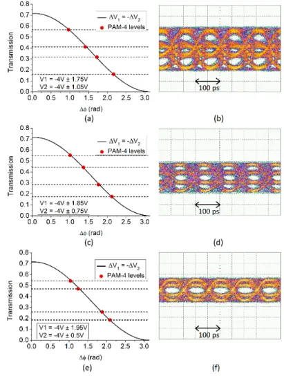
First, we show in Fig. 5 the eye diagrams that are obtained for different peak-to-peak voltages applied on each arm of a quadrature-biased MZM. On the left panel are reported the equivalent modeling, showing a good correlation of the simulated levels with the experimental results for each of the voltage couples used in the experimental setup. It can be seen from Figs. 5(c) and 5(d) that equally spaced levels can be obtained for a voltage ratio of 2.47, which is different from the optimum ratio of 1.74 mentioned in Section 3. This comes from the fact that the ratio of 1.74 fulfills both the even-spacing and the maximum extinction ratio conditions, whereas in the eye diagrams represented in Figs. 5(c) and 5(d) the extinction ratio is limited.
BER measurements were performed at 20 Gb/s using an error analyzer (EA) designed for conventional binary modulation using the method described in [7,35]. The applied peak-to-peak voltages were set to 7 V and 4 V, to benefit from an almost full dynamic range of the transmission while obtaining 4 equally spaced levels. These voltages are slightly lower than the ones stated in Section 3, due to limitations of the RF amplifiers maximum output power, but the voltage ratio of 1.75 is maintained. The received power was swept from −8.5 dBm to 0.5 dBm.
The results were compared to the case of a commercial 32 GHz-bandwidth push-pull LiNbO3 MZM. The modulator was driven by two NRZ electrical streams with peak-to-peak
voltages of 3.25 V and 1.90 V. The static Vπ of this LiNbO3 modulator was measured to be
4 V and the extinction ratio was 9 dB in the O-band. The SOA was removed from the set-up as coupling losses in the LiNbO3 MZM are lower than for the Si modulator. The eye diagrams
at 0 dBm received power corresponding to the two different modulators are plotted in Figs. 6(b) and 6(c).
Fig. 5. Simulated transmission levels (a) (c) (e) and corresponding measured eye diagrams (b) (d) (f) for different applied voltages.
From Fig. 6(a) it can be seen that the power penalty of the silicon device is about 2 dB in comparison with the LiNbO3 modulator in the O-band at a BER of 2.1 × 10⁻⁴. This penalty
can be explained by the lower bandwidth of the silicon modulator in comparison with the LiNbO3 MZM, and the additional noise due to the necessity of using an SOA for the silicon
MZM, because of grating coupler losses. With the Si modulator, the BER is below the hard-decision forward error correction (HD FEC) threshold of 3.8 × 10⁻³ at an average received
power of −6 dBm and under the KP4 FEC threshold of 2.2 × 10⁻⁴ for an average received
Fig. 6. (a) 20-Gb/s BER versus average received power for the Si MZM, compared to a LiNbO3 MZM. (b) Eye diagram of the Si MZM. (c) Eye diagram of the LiNbO3 MZM.
5. Conclusion
DAC-less modulators for PAM-4 generation have been a topic of increasing interest over the past years within the silicon photonics community. We experimentally demonstrate an O-band 20 Gb/s PAM-4 generation using a simple silicon MZM driven by two independent binary streams. Interestingly, this generation method can be applied to higher bitrates, up to 100 Gbit/s, by phase shifter optimization. Modeling has been used to evaluate the influence of the voltages applied on each arm to the output optical transmission levels. By doing so it is possible to benefit from the full dynamic range of the transmission, while obtaining 4 equally spaced levels. The BER obtained with the Si PAM-4 modulator is below the KP4 FEC threshold of 2.2 × 10⁻⁴ for an average received power of −3.4 dBm and corresponds to a
penalty of 2 dB compared to a commercial push-pull LiNbO3 MZM. Funding
H2020 LEIT Information and Communication Technologies European project Cosmicc (H2020-ICT-27-2015-688516).
References
1. W. Shi, Y. Xu, H. Sepehrian, S. LaRochelle, and L. A. Rusch, “Silicon photonic modulators for PAM transmissions,” J. Opt. 20, 083002 (2018).
2. IEEE P802.3bs 400 GbE Task Force, http://www.ieee802.org/3/bs/index.html.
3. H. Zeng, X. Liu, S. Megeed, A. Shen, and F. Effenberger, “Digital signal processing for high-speed fiber-wireless convergence,” J. Opt. Commun. Netw. 11(1), A11–A19 (2019).
4. X. Wu, B. Dama, P. Gothoskar, P. Metz, K. Shastri, and S. Sunder, J. Van de Spiegel, Y. Wang, M. Webster, and W. Wilson, “A 20Gb/s NRZ/PAM-4 1V transmitter in 40nm CMOS driving a Si-photonic modulator in 0.13µm CMOS,” in Proceedings of IEEE International Solid-State Circuit Conference (IEEE, 2013), pp. 128– 129.
5. S. Zhou, H. T. Wu, K. Sadeghipour, C. Scarcella, C. Eason, M. Rensing, M. J. Power, C. Antony, P. O’Brien, P. D. Townsend, and P. Ossieur, “Optimization of PAM-4 transmitters based on lumped silicon photonic MZMs for high-speed short-reach optical links,” Opt. Express 25(4), 4312–4325 (2017).
6. M. Mazzini, M. Traverso, M. Webster, C. Muzio, S. Anderson, P. Sun, D. Siadat, D. Conti, A. Cervasio, S. Pfnuer, J. Stayt, M. Nyland, C. Togami, K. Yanushefsky, and T. Daugherty, “25GBaud PAM-4 error free transmission over both single mode fiber and multimode in QSFP form factor based on silicon photonics,” in Optical Fiber Communication Conference and Exhibition (Optical Society of America, 2015), paper Th5B.3.
7. C. Xiong, D. M. Gill, J. E. Proesel, J. S. Orcutt, W. Haensch, and W. M. J. Green, “Monolithic 56Gb/s silicon photonic pulse-amplitude modulation transmitter,” Optica 3(10), 1060–1065 (2016).
8. T. N. Huynh, N. Dupuis, R. Rimolo-Donadio, J. E. Proesel, D. M. Gill, C. W. Baks, A. V. Rylyakov, C. L. Schow, W. M. J. Green, and B. G. Lee, “Flexible transmitter employing silicon-segmented Mach-Zehnder modulator with 32-nm CMOS distributed driver,” J. Lightwave Technol. 34(22), 5129–5136 (2016). 9. S. Moazeni, S. Lin, M. Wade, L. Alloatti, R. J. Ram, M. Popović, and V. Stovanović, “A 40-Gb/s PAM-4
transmitter based on a ring-resonator optical DAC in 45-nm SOI CMOS,” IEEE J. Solid-State Circuits 52(12), 3503–3516 (2017).
10. M. Chagnon, M. Osman, M. Poulin, C. Latrasse, J. F. Gagné, Y. Painchaud, C. Paquet, S. Lessard, and D. Plant, “Experimental study of 112 Gb/s short reach transmission employing PAM formats and SiP intensity modulator at 1.3 μm,” Opt. Express 22(17), 21018–21036 (2014).
11. A. Samani, M. Chagnon, D. Patel, V. Veerasubramanian, S. Ghosh, M. Osman, Q. Zhong, and D. Plant, “A low-voltage 35-GHz silicon photonic modulator-enabled 112-Gb/s transmission system,” IEEE Photonics J. 7(3), 1– 13 (2015).
12. D. Patel, A. Samani, V. Veerasubramanian, S. Ghosh, and D. Plant, “Silicon photonic segmented modulator-based electro-optic DAC for 100Gb/s PAM-4 Generation,” IEEE Photonics Technol. Lett. 27(23), 2433–2436 (2015).
13. A. Samani, M. Chagnon, E. El-Fiky, D. Patel, M.Jacques, V. Veerasubramanian, and D. Plant, “Silicon photonics modulators architectures for multi-level signal generation and transmission,” in Optical Fiber Communication Conference and Exhibition (Optical Society of America, 2017), paper Tu2H.4.
14. A. Samani, V. Veerasubramanian, E. El-Fiky, D. Patel, and D. Plant, “A silicon photonic PAM-4 modulator based on dual-parallel Mach-Zehnder interferometers,” IEEE Photonics J. 8(1), 1–10 (2016).
15. A. Samani, D. Patel, M. Chagnon, E. El-Fiky, R. Li, M. Jacques, N. Abadía, V. Veerasubramanian, and D. V. Plant, “Experimental parametric study of 128 Gb/s PAM-4 transmission system using a multi-electrode silicon photonic Mach Zehnder modulator,” Opt. Express 25(12), 13252–13262 (2017).
16. L. Zheng, J. Ding, S. Shao, L. Zhang, and L. Yang, “Silicon PAM-4 optical modulator driven by two binary electrical signals with different peak-to-peak voltages,” Opt. Lett. 42(11), 2213–2216 (2017).
17. S. Shao, J. Ding, L. Zheng, K. Zou, L. Zhang, F. Zhang, and L. Yang, “Optical PAM-4 signal generation using a silicon Mach-Zehnder optical modulator,” Opt. Express 25(19), 23003–23013 (2017).
18. Z. Xing, A. Samani, M. Xiang, E. El-Fiky, T. M. Hoang, D. Patel, R. Li, M. Qiu, M. G. Saber, M. Morsy-Osman, and D. V. Plant, “100 Gb/s PAM4 transmission system for datacenter interconnects using a SiP ME-MZM based DAC-less transmitter and a VSB self-coherent receiver,” Opt. Express 26(18), 23969–23979 (2018).
19. M. Li, L. Wang, X. Li, X. Xiao, and S. Yu, “Silicon intensity Mach-Zehnder modulator for single lane 100Gb/s applications,” Photon. Res. 6(2), 109–116 (2018).
20. O. Dubray, M. A. Seyedi, C. H. Chen, B. Charbonnier, A. Descos, M. Fiorentino, R. G. Beausoleil, and S. Menezo, “30Gbit/s PAM-4 transmission by modulating a dual silicon ring resonator modulator,” in Proceedings of IEEE Optical Interconnects Conference (IEEE, 2016), pp. 6–7.
21. R. Dubé-Demers, S. LaRochelle, and W. Shi, “Low-power DAC-less PAM-4 transmitter using a cascaded microring modulator,” Opt. Lett. 41(22), 5369–5372 (2016).
22. R. Dubé-Demers, S. LaRochelle, and W. Shi, “Ultrafast pulse-amplitude modulation with a femtojoule silicon photonic modulator,” Optica 3(6), 622–627 (2016).
23. R. Li, D. Patel, E. El-Fiky, A. Samani, Z. Xing, M. Morsy-Osman, and D. V. Plant, “High-speed low-chirp PAM-4 transmission based on push-pull silicon photonic microring modulators,” Opt. Express 25(12), 13222– 13229 (2017).
24. R. Li, D. Patel, A. Samani, E. El-Fiky, Y. Wang, Z. Xing, L. Xu, and D. Plant, “Analysis and experimental study of a silicon single MRM-assisted MZI PAM-4 modulator,” IEEE Photonics J. 9(6), 1–7 (2017).
25. R. Li, D. Patel, A. Samani, E. El-Fiky, Z. Xing, M. Morsy-Osman, and D. Plant, “Silicon photonic ring-assisted MZI for 50Gb/s DAC-less and DSP-free PAM-4 transmission,” IEEE Photonics Technol. Lett. 29(12), 1046– 1049 (2017).
26. M. S. Hai, M. M. P. Fard, and O. Liboiron-Ladouceur, “A low-voltage PAM-4 SOI ring-based modulator,” in Proceedings of IEEE Photonics Conference (IEEE, 2014), pp. 194–195.
27. M. S. Hai, M. M. P. Fard, and O. Liboiron-Ladouceur, “A ring-based 25 Gb/s DAC-less PAM-4 modulator,” IEEE J. Sel. Top. Quantum Electron. 22(6), 123–130 (2016).
28. R. Li, D. Patel, E. El-Fiky, A. Samani, Z. Xing, Y. Wang, and D. V. Plant, “Silicon photonic dual-drive MIM based 56 Gb/s DAC-less and DSP-free PAM-4 transmission,” Opt. Express 26(5), 5395–5407 (2018). 29. R. C. Figueiredo, A. L. N. Souza, S. M. Ranzini, A. Chiuchiarelli, L. H. H. Carvalho, and J. D. Reis,
“Investigation of 56-GBd PAM4 Bandwidth and Chromatic Dispersion Limitations for Data Center Applications,” in Proceedings of 2017 SBMO/IEEE MTT-S International Microwave and Optoelectronics Conference (IMOC), (IEEE, 2017) pp. 1–5.
30. D. Perez-Galacho, L. Bramerie, C. Baudot, M. Chaibi, S. Messaoudène, N. Vulliet, L. Vivien, F. Bœuf, C. Peucheret, and D. Marris-Morini, “QPSK modulation in the O-band using a single dual-drive Mach-Zehnder silicon modulator,” J. Lightwave Technol. 36(18), 3935–3940 (2018).
31. C. Baudot, A. Fincato, D. Fowler, D. Perez-Galacho, A. Souhaité, S. Messaoudène, R. Blanc, C. Richard, J. Planchot, C. De-Buttet, B. Orlando, F. Gays, C. Mezzomo, E. Bernard, D. Marris-Morini, L. Vivien, C. Kopp,
and F. Boeuf, “Daphne silicon photonics technological platform for research and development on WDM applications,” Proc. SPIE 9891, 98911D (2016).
32. D. Perez-Galacho, C. Baudot, T. Hirtzlin, S. Messaoudène, N. Vulliet, P. Crozat, F. Boeuf, L. Vivien, and D. Marris-Morini, “Low voltage 25Gbps silicon Mach-Zehnder modulator in the O-band,” Opt. Express 25(10), 11217–11222 (2017).
33. G. Rasigade, D. Marris-Morini, M. Ziebell, E. Cassan, and L. Vivien, “Analytical model for depletion-based silicon modulator simulation,” Opt. Express 19(5), 3919–3924 (2011).
34. D. Pérez-Galacho, D. Marris-Morini, R. Stoffer, E. Cassan, C. Baudot, T. Korthorst, F. Boeuf, and L. Vivien, “Simplified modeling and optimization of silicon modulators based on free-carrier plasma dispersion effect,” Opt. Express 24(23), 26332–26337 (2016).
35. K. Szczerba, P. Westbergh, J. Karout, J. Gustavsson, Å. Haglund, M. Karlsson, P. Andrekson, E. Agrell, and A. Larsson, “30 Gbps 4-PAM transmission over 200 m of MMF using an 850 nm VCSEL,” Opt. Express 19(26), B203–B208 (2011).