Suspended Carbon Nanotube Beams Fabricated by a Low
Temperature Surface Micromachined Process for
Humidity and Gas Sensing
by
Shiva Ram ARUNACHALAM
MANUSCRIPT BASED THESIS PRESENTED TO ÉCOLE DE
TECHNOLOGIE SUPÉRIEURE IN PARTIAL FULFILLMENT FOR THE
DEGREE OF DOCTOR OF PHILOSOPHY
Ph.D.
MONTREAL, MARCH 29, 2020
ÉCOLE DE TECHNOLOGIE SUPÉRIEURE UNIVERSITÉ DU QUÉBEC
This Creative Commons licence allows readers to download this work and share it with others as long as the author is credited. The content of this work can’t be modified in any way or used commercially.
BOARD OF EXAMINERS
THIS THESIS HAS BEEN EVALUATED BY THE FOLLOWING BOARD OF EXAMINERS
Mr. Frédéric Nabki, Thesis Supervisor
Department of Electrical Engineering, École de Technologie Supérieure
Mr. Ricardo Izquierdo, Thesis Co-supervisor
Department of Electrical Engineering, École de Technologie Supérieure
Mr. Guy Gauthier, President of the Board of Examiners
Department of Systems Engineering, École de Technologie Supérieure
Mr. Ricardo Zednik, Member of the jury
Department of Mechanical Engineering, École de Technologie Supérieure
Mr. Thomas Szkopek, External Evaluator McGill University
THIS THESIS WAS PRESENTED AND DEFENDED
IN THE PRESENCE OF A BOARD OF EXAMINERS AND PUBLIC 26 FEBRUARY 2020
ACKNOWLEDGMENT
Neither this Ph.D., nor these past five years in Montreal, nor me would be the same without the help and company of many people.
First, I would like to express my sincere gratitude to my research supervisor Professor Frederic Nabki and my co-supervisor Professor Ricardo Izquierdo, for giving me the opportunity to pursue a Ph.D. and keeping faith in me through some challenging times. I will never forget your words of encouragement and support. This Ph.D. would not have been possible without your guidance, knowledge and intuitive insights. Thank you for teaching me, inspiring me and patiently listening to me. I could not have asked for better guidance. I am especially thankful to Professor Nabki for continually pushing me towards excellence in my research. His work-ethic and passion for science is infectious. It is something that I will strive to carry with me throughout my professional life.
Secondly, I would like to thank all the members of the thesis committee for their encouragement, time and insightful comments. I would also like to express my sincere gratitude to the technical staff at ETS and UQAM, Alexandre Robichaud and Normand Gravel for helping me train on the lab equipment and addressing any difficulties that I may have faced. Without their support, thesis research project would not have been possible. My friends who formed a large part of my life in Montreal and have become more like family: Anubha, Michiel, Lakshay, Pankaj, Devika, Mohammed and many others. Thank you for all the love and support. I will fondly remember the conversations and parties that we had over the years
Finally, and most importantly, I want to thank my family, my biggest pillars of strength, support and inspiration. I would not be where I am today if not for their sacrifice, encouragement, patience and advice when I needed it most. Although I live thousands of miles away, I feel their love, warmth and presence constantly and it helps me push through life’s obstacles. I wouldn’t be who I am if it wasn’t for you.
Faisceaux de nanotubes de carbone suspendus fabriqués par un procédé micromachiné en surface à basse température pour la détection d'humidité et de gaz
Shiva Ram ARUNACHALAM
RÉSUMÉ
Le monde dans lequel nous vivons aujourd'hui est connecté de plus de façons que nous ne pouvons l'imaginer. Les appareils intelligents et les réseaux sont au cœur de notre vie quotidienne. L'avènement de l'Internet des objets et de l'industrie 4.0 nécessite différents types de capteurs fonctionnants conjointement. Gardant cela à l'esprit, cette thèse explore l'application des nanotubes de carbone à simple paroi en suspension pour la détection de gaz. Les détecteurs de gaz sont utilisés dans une variété d'environnements tels que les hôpitaux, les navettes spatiales et les cuisines domestiques pour détecter et empêcher les fuites de gaz dangereux. Une variété de matériaux tels que les polymères, la céramique et les oxydes métalliques et les mécanismes de détection ont été utilisés pour identifier divers gaz. Plus récemment, les nanotubes de carbone ont suscité une attention considérable pour les applications de détection de gaz en raison de leurs excellentes propriétés électriques et de leur facilité de modification de surface. Avec les progrès des techniques de production, le coût de production des nanotubes de carbone a considérablement diminué, ce qui a permis le développement de capteurs de gaz à base de nanotubes de carbone. Bien que plusieurs capteurs de gaz à base de nanotubes de carbone aient été étudiés dans le passé, la structure globale du dispositif reste globalement similaire. De plus, ces dispositifs offrent souffrent de grands effets hystérétiques, souvent en raison de l'effet du substrat sur le mécanisme de détection global, ce qui peut conduire à des sorties de mesure peu fiables.
Ce travail vise à résoudre le problème de l'hystérésis en utilisant des nanotubes de carbone en suspension et ainsi isoler l'élément de détection des effets du substrat. Pour ce faire, tout d'abord, un procédé de micro-usinage de surface à basse température est développé pour obtenir des dispositifs suspendus. Une fois le processus bien développé, le dispositif suspendu est utilisé pour détecter l'humidité. Les performances du dispositif suspendu sont comparées à celles d'un dispositif non suspendu pour démontrer les avantages des nanotubes de carbone suspendus.
Ensuite, les mesures de performance du capteur suspendu sont améliorées en fonctionnalisant chimiquement les nanotubes pour les rendre plus sensibles à la vapeur d'eau. Les nanotubes sont obtenus dans le commerce, pré-fonctionnalisés et utilisés dans le processus de fabrication. Une étude comparative entre les capteurs à base de nanotubes fonctionnalisés suspendus et non suspendus est également réalisée. Enfin, la conception de l'appareil a été modifiée pour fabriquer un capteur de gaz d'ionisation basé sur des nanotubes de carbone suspendus alignés horizontalement. Le potentiel d'ionisation de divers gaz est identifié et d'autres paramètres tels que la répétabilité, la stabilité à long terme, etc. ont été étudiés.
Suspended Carbon Nanotube Beams Fabricated by a Low temperature Surface Micromachined Process for Humidity and Gas sensing
Shiva Ram ARUNACHALAM
ABSTRACT
The world we live in today is connected in more ways than we can imagine. Smart devices and networks form the core of our everyday lives. The advent of the Internet of Things and Industry 4.0, which are terms defined to make the world around us more connected via the internet at a domestic and industrial setting respectively, necessitates various kinds of sensors working in conjunction with each other. Keeping this in mind, this thesis explores the application of Suspended Single walled Carbon Nanotubes for Gas Sensing. Gas Sensors are used in a variety of environments such as hospitals, space shuttles and domestic kitchens to detect and prevent the leakage of hazardous gases. A variety of materials such as Polymers, ceramics and metal oxides and detection mechanisms have been used to identify various gases. More recently, Carbon nanotubes have garnered considerable attention for gas sensing applications due to their excellent electrical properties and ease of surface modification. With advancements in production techniques, the cost of Carbon Nanotube production has reduced significantly which has enabled the development of Carbon Nanotube based gas sensors. Although multiple Carbon Nanotube based gas sensors have been studied in the past, the overall device structure remains broadly similar. Additionally, these devices offer suffer from large hysteretic effects, often because of the effect of the substrate on the overall sensing mechanism, which can lead to unreliable measurement outputs.
This work aims to solve the issue of hysteresis by using suspended Carbon Nanotubes and thereby isolating the sensing element from the effects of the substrate. To do this, first, a low temperature surface micromachining process is developed to obtain suspended devices. Once the process is well developed, the suspended device is used to detect humidity. The performance of the suspended device is compared to a non-suspended device to demonstrate the advantages of suspended Carbon nanotubes.
Next, the performance metrics of the suspended sensor are improved by chemically functionalizing the nanotubes to make them more sensitive to water vapor. The nanotubes are obtained commercially, pre-functionalized, and used in the fabrication process. A comparative study between suspended and non-suspended functionalized nanotube-based sensors is also done. Lastly, the device design has been modified to fabricate an ionization gas sensor based on horizontally aligned suspended carbon nanotubes. The ionization potential of various gases is identified and other parameters such as the repeatability, long term stability, etc. have been studied.
TABLE OF CONTENTS
Page
INTRODUCTION ...1
CHAPTER 1 INTRODUCTION TO MEMS TECHNOLOGY ...7
1.1 Microelectromechanical Systems (MEMS) ...7
1.2 MEMS Technology ...8
1.3 Materials used in MEMS ...10
1.3.1 Silicon ... 10
1.3.2 Polymers ... 10
1.3.3 Ceramics ... 11
1.4 Fundamental MEMS Techniques ...11
1.4.1 Lithography ... 12 1.4.2 Bulk Micromachining ... 13 1.4.3 Surface Micromachining ... 14 1.4.4 LIGA ... 15 1.4.5 Wafer Bonding ... 16 1.5 Summary ...17
CHAPTER 2 CARBON NANOTUBES – PROPERTIES AND APPLICATIONS ...19
2.1 Introduction ...20
2.2 Carbon Nanotube Basics ...21
2.3 Carbon Nanotubes: Structure and Properties ...21
2.4 Electrical Properties of Carbon Nanotubes ...23
2.5 Mechanical Properties of Carbon Nanotubes ...25
2.6 Applications of Carbon Nanotubes ...27
2.7 Carbon Nanotubes: Applications in MEMS and NEMS ...29
2.8 Carbon Nanotube Application Challenges ...30
CHAPTER 3 GAS SENSING USING CARBON NANOTUBES ...31
3.1 Introduction ...32
3.2 Pristine Carbon Nanotube Gas Sensors ...32
3.3 Suspended Carbon Nanotubes for Gas Sensing ...35
3.4 Humidity Sensing...37
3.5 Carbon Nanotubes for Humidity Sensing ...38
3.6 Carbon Nanotube based Ionization Gas Sensors ...41
CHAPTER 4 SUSPENDED CARBON NANOTUBES FOR
HUMIDITY SENSING ...45
4.1 Abstract ...46
4.2 Introduction ...46
4.3 Materials and Methods ...48
4.4 Results and Discussion ...51
4.5 Conclusion ...58
CHAPTER 5 LOW-HYSTERESIS AND FAST RESPONSE TIME HUMIDITY SENSORS USING SUSPENDED CARBON NANOTUBES ...61
5.1 Abstract ...62
5.2 Introduction ...62
5.3 Materials and Methods ...64
5.4 Results ...65
5.4.1 Humidity Response ... 66
5.5 Response time, Recovery time and Sensitivity ...67
5.6 Temperature Study ...70
5.7 Long term Stability ...71
5.8 Conclusions ...72
CHAPTER 6 IONIZATION GAS SENSOR USING SUSPENDED CARBON NANOTUBE BEAMS ...75
6.1 Abstract ...76
6.2 Introduction ...76
6.3 Materials and Methods ...79
6.3.1 Test Setup... 81 6.4 Results ...82 6.5 Discussion ...87 6.6 Conclusions ...88 CONCLUSION… ...89 LIST OF PUBLICATIONS ...95 BIBLIOGRAPHY ...97
LIST OF TABLES
Page
Table 1.1 A Brief History of MEMS ...8 Table 5.1 Comparison of the Response and Recovery times of different CNT
LIST OF FIGURES
Page Figure 1.1 (a) MEMS sales in the USA for 2015 and 2016, and,
(b) SEM Micrograph of a typical MEMS device, and, (c) The world’s smallest guitar, fabricated by MEMS
fabrication technologies ...9 Figure 1.2 MEMS Components ...11 Figure 1.3 Lithography in MEMS ...12 Figure 1.4 (a) Isotropic, and
(b) Anisotropic etch profile, and,
(c) Cantilever beam fabricated by Bulk Micromachining ...13 Figure 1.5 (a) Schematic of Surface Micromachining and,
(b) SEM image of a comb-drive fabricated by a
surface micromachining process ...14 Figure 1.6 Schematic of the LIGA Process. ...15 Figure 2.1 Types of CNTs based on chirality, (a) Armchair, (b) Zigzag and
(c) Chiral ...21 Figure 2.2 MWCNT Structure ...22 Figure 2.3 Electronic band structure of CNTs (a) (5,5), (b) (9,0) and,
(c) (10,0) obtained by folding of a graphene sheet ...23 Figure 2.4 Conductivity of various types of SWNT films as a function of
film thickness ...24 Figure 2.5 (a) Bicycle made of CNT reinforced metal and,
(b) AFM image of a CNT FET ...27 Figure 2.6 (Top) A false-colored SEM image of a suspended device and,
(Bottom) Device geometry ...29 Figure 3.1 (a) Response of SWNTs to NO2 and NH3 and,
(b) Device response of the ChemFET Sensor ...32 Figure 3.2 (a) Hysteresis free operation of a suspended NO2 gas sensor and,
(b) SEM micrograph of an individual suspended MWCNT acting as an
VII
Figure 3.3 Schematic of the interdigitated humidity sensor ...38 Figure 3.4 Normalized response of MWCNT sensor and the Honeywell sensor ...39 Figure 3.5 Breakdown Voltages of various gases for the MEMS based
ionization sensor ...41 Figure 4.1 Process flow Schematic ...48 Figure 4.2 (a) and (b) Suspended beams with different suspension lengths,
(c) A normal Non-suspended nanotube beam, and,
(d) Networks of nanotubes that comprise the beam ...51 Figure 4.3 (a) Schematic of the test setup, and,
(b) Photograph of the device inside the test chamber ...52 Figure 4.4 (a, b) Humidity response and Hysteresis for suspended carbon nanotubes
(36 µm and 72 µm respectively), and,
(c, d) humidity response and hysteresis for suspended carbon nanotubes
(36 µm and 72 µm respectively) ...53 Figure 4.5 (a) Rise time and (b) fall times of suspended carbon nanotubes, and,
(c) Rise time and, (d) fall times of non-suspended carbon nanotubes The humidity was varied from 15% to 98% in steps of
10% RH increases every 20 s ...55 Figure 4.6 Repeatability of (a) suspended carbon nanotubes, and,
(b) non-suspended carbon nanotubes ...56 Figure 4.7 Long-term stability of (a) suspended sensors and,
(b) non-suspended sensors of 36 µm suspension ...56 Figure 4.8 Sensitivities of suspended and non-suspended sensors ...57 Figure 5.1 (a) Schematic of the suspended CNT beam and (b) SEM Micrograph ...64 Figure 5.2 (a) Plot of the humidity response of the suspended CNTs, and,
(b) Plot of the humidity response of the non-suspended CNTs. The hysteresis characteristic is also shown.
The insets in each figure show the average hysteresis profile of
6 identical devices measured under similar testing conditions ...66 Figure 5.3 Response time and (b) recovery time of the suspended CNTs
(c) response time and (d) recovery time of the non-suspended CNTs
Figure 5.4 (a) Repeatability measurement over four humidity cycles
for the suspended CNTs, and, (b) for the non-suspended CNTs ...68 Figure 5.5 Sensitivity factors of suspended CNTs vs. non-suspended CNTs ...69 Figure 5.6 Resistance vs. temperature for suspended and non-suspended CNTs ...70 Figure 5.7 (a) Resistance as a function of time for suspended CNTs, indicating device
stability, and
(b) recovery time to 15% RH of the suspended CNTs after exposure to
98% RH for 24 h ...71 Figure 6.1 (a) Process Flow Schematic and,
(b) Schematic of the cross section of the device. ...78 Figure 6.2 (a) SEM Micrograph of the device and,
(b) High Magnification SEM micrograph of the CNTs comprising the beam ...79 Figure 6.3 Photograph of the test setup used for the measurements showing the gas
chamber, the multimeter and the computer for data acquisition. ...81 Figure 6.4 Breakdown signatures of Various gases as tested ...82 Figure 6.5 (a) Gas concentration vs breakdown voltage which shows that the
breakdown voltage of the gas is independent of the gas concentration, and (b) discharge current increases as a function of concentration due to
increasing gas molecules available for conduction. ...82 Figure 6.6 (a) Breakdown Voltage variation with different gas-air mixtures and
(b) Dynamic sensing Curves of the sensor for N2...83
Figure 6.7 Sensing mechanism with a positive nanotip: (I) Nanotip Ionization,
(II) Impact Ionization and (III) Electron Recombination ...84 Figure 6.8 (a) Effect of inter-electrode distance on the Breakdown Voltage, and,
LIST OF ABREVIATIONS
MEMS Microelectromechanical Systems IC Integrated Circuits
CNTs Carbon Nanotubes
SWCNT Single-walled Carbon Nanotubes MWCNT Multi-walled Carbon Nanotubes NEMS Nanoelectromechanical Systems in3 Cubic inch
CMOS Complementary metal-oxide semiconductor PMMA Poly Methyl Methacrylate
TEM Transmission Electron Microscope nm Nanometers
FET Field Effect Transistor
ChemFET Chemical Field Effect Transistor MHz Megahertz
CVD Chemical Vapor Deposition ppm Parts per Million
ppb Parts per billion
PAA Polyacrylic acid RH Relative Humidity DI Deionized
SEM Scanning Electron Microscope min Minutes
rpm Rounds per minute s Second
VOCs Volatile Organic Compounds SDS Sodium Dodecyl Sulfate Wt% Weight %
Tpa Tera Pascal DC Direct current
DRIE Deep Reactive Ion Etching Isd Source-drain current
LIST OF SYMBOLS
µm Micrometers °C Degrees Celsius GaAs Gallium Arsenide InP Indium Phosphide V Volts eV Electron-volt K Kelvin mK milli-Kelvin C Chiral Vector d Diameter σ Stress σc Film thickness ε Strain σs Tensile Strength
Sm-1 Siemens per meter
aN Atto-newton
cm2V-1s-1 centimeter squared per volt per second
Cr Chromium Au Gold Ar Argon He Helium N2 Nitrogen CO Carbon Monoxide Si Silicon
COOH Carboxylic acid group HF Hydrofluoric acid KOH Potassium Hydroxide HNO3 Nitric acid
CO2 Carbon dioxide
g Gram kΩ Kilo-ohm Gpa Giga-Pascal R Resistance
RH Resistance at any measured humidity
Ro Baseline resistance
INTRODUCTION Motivation
During the past two decades, the field of Micro-electromechanical systems (MEMS) has attracted significant attention from academic researchers as well as the electronics industry. MEMS can be described as a process technology that can be used to create miniature components ranging in size from a few micrometers to a few millimeters. These miniature devices can be used in various applications such as sensing, actuation, etc. Over the years, MEMS has become an interdisciplinary field in which expertise from different areas such as materials science, electrical engineering, IC design, etc. MEMS technology has matured to the point where its applications can now be found in a variety of systems ranging from automotive, medical and defense applications. Some everyday MEMS devices that we come across include accelerometers in automobile airbags, printheads for ink-jet printers, etc. MEMS is one of the most promising technologies of the 21st century and has the potential to revolutionize many
aspects of industrial and consumer products.
Gas sensors enable the detection of various gaseous components in the ambient air. Gas sensors find their use in a variety of applications such as process control and packaging facilities, domestic kitchens, environment control in automobiles and space shuttles, etc. Gas sensors primarily consist of a sensing element and a component to transfer the signal, namely, a transducer. Various sensing elements such as metal oxides, polymers, biomaterials, etc. have been used for gas detection (Baratto et al. 2005; Yang et al. 1999). The sensing mechanism is a characteristic of change in the material properties due to the interaction between the analyte and the sensing element. The type of interaction can be chemical or physical depending on the type of analyte-sensor interaction. Transduction mechanisms include optical, capacitive, resistive, etc. (Barone et al. 2004; Yang et al. 1999). Gas sensors are not the only tools that can be used for gas detection and analysis. Tools like Gas chromatography, Spectrometry, etc. have also been used extensively for a similar purpose (Ballschmiter and Zell 1980). However, these tools are cumbersome to operate, expensive and can have sub-optimal performance in some conditions.
Carbon Nanotubes (CNTs), which are essentially rolled up sheets of Graphene, have been actively used as gas sensing elements in the past few years, owing to their excellent electrical properties. The ability to tailor the sensitivity of CNTs to specific gases by chemical functionalization of the sidewalls makes them suitable candidates for gas sensing applications. CNTs have been used to detect gases such as NH3, CO, etc. CNT sensors have demonstrated
fast response and recovery times, long shelf life and high selectivity which are essential factors to make a good gas sensor. Thus, the electrical properties of CNTs in combination with MEMS fabrication technologies has the potential to result in high performance, cost-effective gas sensors which can be widely used in various applications.
Problem Statement
Although CNTs make for a great sensing material, CNT based gas sensors often suffer from hysteretic effects, often due to the role played by the substrate in the overall sensing mechanism. A detailed study by Soares et al. (Soares and Jorio 2012) have shown that the substrate sometimes limits the charge transfer in case of chemical sensors. Hysteresis often leads to unreliable measurements and subsequently unreliable results, which are not desirable. Interestingly, not a lot of research has been done to study and eliminate hysteretic effects in gas sensors. One way to eliminate the unwanted effects is to use a suspended architecture wherein the sensing element is suspended above the substrate. Suspended CNT devices have been studied and published previously to study the intrinsic properties of CNTs such as transport mechanism and scattering phenomena. Muoth et al. (Muoth et al. 2010) first fabricated a hysteresis free CNT transistors. The hysteresis free operation of the transistors in this work is attributed to the absence of substrate effects on the CNT. (Chikkadi et al. 2014a) in their work further proved that a suspended architecture is instrumental in eliminating hysteretic effects.
Although suspended CNT sensors exist in literature, their application to gas sensing has been limited to detecting NO2 (Chikkadi, Muoth, and Hierold 2013). Thus, it would be interesting
to see if combining a suspended architecture and the intrinsic properties of CNTs can solve the issue of hysteresis and lead to improved reliability.
3
It will also be interesting to see if adopting a suspended architecture also improves other aspects of device performance such as the response time, recovery time and sensitivity. Fabrication of suspended devices involves use of expensive equipment such as vapor deposition tools and lithography tools such as e-beam lithography which also adds to the time consumption. Even by using these expensive techniques, obtaining a usable device yield and repeatability remains a challenge.
Thus, this Ph.D. work aims to study and address the problem of device reliability while also trying to improve other sensor aspects such as response time, long term stability and sensitivity. The primary focus of research in this Ph.D. is the design and fabrication of suspended CNT beams using a photoresist sacrificial layer by a low-temperature process that is integrable with above IC processes aiding in maximum sensor integration. To the author’s best knowledge, there has not been an attempt yet to fabricate suspended CNT beam sensors by a low-temperature process.
Research Goals
MEMS fabrication technology has been at the forefront of sensor fabrication for the past few years. Bulk and surface micromachining techniques have been used to fabricate various types of sensors over the past few decades, with bulk micromachining being preferred in the industry since it results in cleaner devices, without stiction issues and high aspect ratio structures (Aimi et al. 2004). The fabrication costs associated with bulk micromachining are often on the higher side due to the use of dry etch setups and expensive lithography machines. However, the costs involved can be justified in the long run due to mass production and market demand. However, bulk micromachining is not amenable to monolithic integration above ICs which is why this research work was done by surface micromachining.
The primary aim of this Ph.D. work is to develop suspended CNT based gas sensors based on a MEMS surface micromachining process. Specifically, the inherent advantages of suspended CNTs for gas sensing is studied and demonstrated.
One of the objectives of the fabrication process is to have a low temperature budget preferably under 115°C and without the use of any expensive equipment like e-beam and chemical vapor deposition and by using a photoresist as a sacrificial layer.
The development of the microfabrication process and fabrication of a device constitutes the first part of the project. Further, the device is tested under humidity to gauge its response. Then, the device design and fabrication process are evolved by placing a metal electrode underneath the suspended beam, and thus an ionization sensor based on suspended CNTs is fabricated and tested. This further process the versatility of the envisioned fabrication process.
Thus, the main objectives of this thesis can be summarized as follows:
• Identify the challenges with current humidity and gas sensing materials and methods. • Design, fabrication and testing of a novel suspended CNT beam humidity sensor to
eliminate hysteretic effects.
• Improving the performance metrics of the fabricated humidity sensor by using readily obtained chemically functionalized CNTs as the sensing material.
• Evolution of device design to fabricate a CNT based ionization gas sensor.
Thesis Outline
This thesis is organized into 6 chapters.
Chapter 1 aims to familiarize the reader about MEMS techniques and includes discussions
about commonly used materials and MEMS fabrication methodologies.
Chapter 2 gives a brief introduction about CNTs, which is the sensing material used in this
PhD work. The electrical and mechanical properties of CNTs are discussed followed by a brief description of the potential applications of CNTs in various fields such as electronics, energy harvesting and sensing. Finally, the challenges currently facing the commercial application of CNTs is discussed.
5
Chapter 3 discusses the application of CNTs to gas sensing by reviewing various peer
published works. A section discussing the application of suspended CNTs for gas sensing is presented. Further, a section pertaining to humidity sensing is presented with an overview of the most popular materials used, including CNTs is presented. Further, CNT based ionization sensors are reviewed.
Chapter 4 presents a humidity sensor using suspended CNT beams. The developed surface
micromachining-based microfabrication process is described in detail. Then, the humidity sensing capabilities of suspended CNTs is studied and the results are reported. This work constitutes the first journal publication of this Ph.D. work published in MDPI Sensors.
In Chapter 5, a functionalized suspended CNT humidity sensor is presented. In this work, a remarkable improvement in all performance metrics is reported. The CNTs in this work were obtained pre-functionalized to increase their affinity to water vapor directly correlating to the improved performance. This work forms the second journal publication of this Ph.D. work published in MDPI Sensors.
In Chapter 6, a concept for the evolution of the sensor structure and design is presented. This work constitutes the third journal publication. In this work, an ionization sensor based on a suspended CNT beam is fabricated and tested for sensitivity to various gases. This further proves that the developed process can be easily modified and adopted for fabricating different types of sensors. The resultant ionization sensor has good performance metrics and good long-term stability as compared to other works in literature but by eliminating use of any high temperature CNT growth techniques.
CHAPTER 1
INTRODUCTION TO MEMS TECHNOLOGY
The 20th century gave birth to major technological accomplishment such as manned flight,
lasers, information technology, the internet, integrated circuits (ICs) and Microelectromechanical Systems (MEMS). The conception of the transistor using Germanium by John Bardeen and Walter Barttain of Bell Labs in 1947 ignited a spark and research in electrical engineering spiked interest, eventually leading to the field known as Microelectromechanical Systems (MEMS). Soon after the discovery of the transistor, the piezoresistive property of Silicon was discovered and the first silicon strain gauge was fabricated in 1954 followed by its commercialization in 1959 by Kulite Semiconductors. Further, the first Integrated Circuit (IC) was developed by Jack Kilby of Texas Instruments in 1958 consisting of 1 transistor, 3 resistors and 1 capacitor on one Germanium chip. Not long after, Fairchild Semiconductor commercialized the IC after Robert Noyce’s invention of the first Silicon integrated circuit. The 1960’s and 1970’s saw rapid progress in the area of pressure sensors fabricated by etching Si using bulk micromachining. Kurt Petersen of IBM developed a pressure sensor using a Si diaphragm by micromachining. The rate of advancement in MEMS associated technologies has been nothing short of outstanding with applications in displays, sensing, computing, etc., which affect our lives every day.
1.1 Microelectromechanical Systems (MEMS)
Richard Feynman, during his talk at the American Physical Society in 1959 claimed that “There is plenty of room at the bottom”. This famous quote can be credited to the development of cutting-edge technologies at the micro and nano scale. Feynman pointed out that there was lack of research to explore the micro-dimension and that it might be of interest to investigate for potential applications. Feynman famously challenged the scientists to print the contents of a page of a book in an area 1/25,000 smaller and to make a working motor measuring less than 1/64 in3.
7
Table 1.1 A Brief History of MEMS
1950’s 1960’s 1970’s 1980’s 1990’s “There’s plenty of room at the Bottom” Silicon Piezoresistive Sensors (Honeywell) Silicon Pressure Transducers (Honeywell) Polysilicon Surface Micromachining Commercial Accelerometer (Analog Devices) Digital Mirror Display Metal Sacrificial Process Resonant gate transistor Integrated Gas Chromatograph Polysilicon Micrometers Optical Network Switch (Lucent) Silicon Gyroscope (Draper Labs) HNA &EDP Etching
Ink Jet Nozzles (IBM) KOH Etching Silicon wafer bonding LIGA RF MEMS Optical MEMS Bio MEMS TMAH Etching Deep Reactive Ion
etching (DRIE)
Consequently, the motor was developed in 1960 by William McLellan (Science and Society 2004) and the book was reproduced by Thomas Newman of Stanford in 1985 (Archives.caltech.edu 2016).
Table 1 shows a brief history of MEMS and significant milestones in the area across each decade. One can clearly notice the significant progress in various areas and applications. Significant developments and innovations based on MEMS devices are still being reported as the technology evolves continuously.
1.2 MEMS Technology
MEMS is the technology of microscopic devices. At the nanoscale, it merges into Nano-electromechanical systems (NEMS). MEMS are also sometimes referred to as microdevices or micro-systems technology. MEMS are made up of components that range in size between 1 and 100 µm in size and the device sizes usually range from micrometers to sometimes a few millimeters. Once the first MEMS device was fabricated and published, a lot of visionary researchers in both academic and industrial domains took notice and immediately began developing a variety of micro-devices such as micro-cantilevers, micro-gears, etc. MEMS systems have been used in devices such as RF switches, sensors, actuators and accelerometers.
With advancements in microfabrication techniques, the field eventually split into a variety of sub-categories such as Radiofrequency MEMS, Optical MEMS, microfluidic MEMS, etc. Figure 1 (a) shows the progression of MEMS device research and sales in the USA for the years 2015 and 2016 in US$ millions. The clear increase in market value of MEMS is mainly due to advancements made in the areas of packaging, device performance and miniaturization.
Figure 1.1 (a) MEMS sales in the USA for 2015 and 2016, and,
(b) SEM Micrograph of a typical MEMS device Taken from Smith et al. (2001), and, (c) The world’s smallest guitar, fabricated by MEMS fabrication technologies
Taken from http://news.cornell.edu/stories/1997/07/worlds-smallest-silicon-mechanical-devices-are-made-cornell
(Consulted in December 2019)
(a)
9
1.3 Materials used in MEMS
Some popular materials used to fabricate MEMS devices are as follows:
1.3.1 Silicon
Silicon is the go-to material for fabrication of MEMS devices. Silicon in crystalline form is a great Hookean material, meaning, it has minimal energy dissipation. This property also contributes to reliability as it suffers from very little fatigue and shows no mechanical hysteresis. The high melting point of 1400°C also makes it a good candidate for high temperature operation. Added to this, the ready availability of high-quality silicon, cost of scaling and the ability to incorporate electronic functionality make silicon an attractive proposition for MEMS applications. Silicon is mostly used as a substrate material in MEMS applications in a single-crystal form. Other compounds of Silicon such as Silicon dioxide, Silicon carbide and Silicon Nitride are also used in various applications. In this work, Silicon has been used primarily as a substrate and is not an active component of the device.
1.3.2 Polymers
Polymers play a major role in MEMS and microelectronics. They can be found in the packaging of IC chips, intermetallic dielectric layers, etc. Polymers are one of the essential elements in microfabrication of MEMS devices as photoresists for lithographic patterning. The ease of processing, relatively low cost and ease of production and high stability makes them a great choice for use in MEMS. Polymers are generally insulators but there are ways like Pyrolysis and metal doping to make them conductive. These conductive polymers are used as substrates in MEMS. Some popular polymers used in cleanrooms include SU-8, an epoxy-based photoresist consisting of 8 epoxy groups, Polymethyl Methacrylate (PMMA), Parylene, etc. This work uses SU-8, a polymer as a sacrificial material to obtain suspended CNT devices.
1.3.3 Ceramics
Ceramics materials like silicon nitride and silicon carbide are also being increasingly used in MEMS fabrication for piezoelectric devices where electrical and mechanical properties are coupled. Electrostatic MEMS are fabricated using ceramic materials owing to their large elastic modulus. Other favorable properties of ceramics include their chemical inertness, resistance to corrosion, etc.
1.4 Fundamental MEMS Techniques
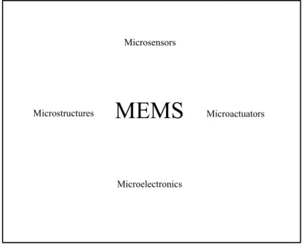
Generally, MEMS can be divided into four major components as shown in Figure 1.2. Most of the times, all the four components are integrated onto a single chip. Micro-sensors detect changes in the environment by measuring changes in mechanical, thermal or chemical properties or phenomena and convert them to an electrical signal. Sensors generally operate by monitoring displacement of structures like beams and diaphragms. These elements are manufactured using several processing techniques, some of which are described briefly in the following section.
MEMS
Microsensors Microactuators Microelectronics Microstructures11
1.4.1 Lithography
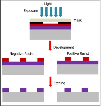
Lithography or photolithography is the process of transferring a pattern on a photomask onto a substrate using a photosensitive polymer. The photosensitive polymer is coated on the substrate using spin coating. Photoresists can be of two types: positive and negative depending on their reaction to UV light. Photolithography is a very common step and, in most cases, one of the first steps in MEMS processing. With the demand for increased resolution in the semiconductor industry, new methods such as X-ray lithography, e-beam lithography ion beam lithography and more recently Extreme UV Lithography have been developed. A schematic of the basic steps for lithography using both positive and negative photoresists is shown in Figure 1.3.
Negative Resist Positive Resist
Light
Mask Exposure
Development
Etching
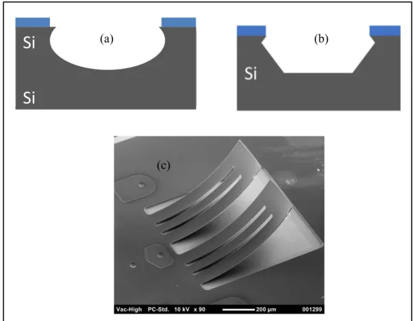
1.4.2 Bulk Micromachining
In Bulk micromachining, the substrate is selectively etched to create microstructures such as micro-cavities, channels. It is a subtractive process and generally, wet etch methods are preferred for cost effectiveness. The etchants used for wet etching can be either isotropic or anisotropic in nature. Isotropic etchants etch in multiple directions within the substrate and are limited by the geometry of the substrate. Examples of isotropic etchants include hydrofluoric acid (HF), Nitric acid (HNO3). Anisotropic etchants, like Potassium Hydroxide (KOH) on the
other hand, etch in one direction depending on the etchant’s affinity to the crystallographic orientation. Dry etching is based on vapor or plasma states of various reactive gases at high temperatures for etching.
Si
Si
(c)
(a) (b)
Figure 1.4 (a) Isotropic, and (b) Anisotropic etch profile, and, (c) Cantilever beam fabricated by Bulk Micromachining
Taken from https://www.memsjournal.com/2011/01/mems-contributions-grow-forthe-control-of-atrial-fibrillation.html (Consulted in December 2019)
13
Reactive Ion Etching, which utilizes additional energy in the form of Radio Frequency power is the most common dry etching technique used. More recently, Deep Reactive Ion Etching (DRIE) is used sometimes to create structures with complex geometries and high aspect ratios. Some examples of devices fabricated by bulk micromachining include pressure sensors, cantilevers and accelerometers.
1.4.3 Surface Micromachining
Deposit Sacrificial layer Pattern
Deposit Structural layer Etch Sacrificial layer
(a)
(b)
Figure 1.5 (a) Schematic of Surface Micromachining and,
(b) SEM image of a com-drive fabricated by a surface micromachining process Taken from Sandia National Laboratories SUMMiT™ Technologies
In surface micromachining, thin films are deposited as structural and sacrificial layers on top of a substrate, making it an additive process. The substrate in this case does not play a major role like in bulk micromachining. Examples of sacrificial layers include polymers, metals, polysilicon, etc. Added structural layers are usually deposited that may vary in thickness from 2 to 5 µm. These layers are generally patterned using photolithography and etched using either wet or dry etching techniques depending on the requirement.
Examples of MEMS devices fabricated by surface micromachining include micromotors, comb drives and springs. An important advantage of surface micromachining over bulk micromachining is that it is compatible with CMOS processing. This compatibility allows integration of mechanical components to logic circuits. Surface micromachining is also cost-effective as compared to bulk micromachining. One major issue that devices suffer is stiction. Close attention should be paid to the compatibility of different layers to reduce the effect of stiction in the devices. Surface micromachining techniques are primarily used for fabrication in this Ph.D. work.
1.4.4 LIGA
Figure 1.6 Schematic of the LIGA Process. Taken from
optics.de/index.php/en/10-hauptkategorie-en/208-15
LIGA, which is acronym for Lithographie, Galvanoformung, Abformung was developed in Germany to overcome the two-dimensionality of Surface Micromachining. LIGA forms a part of High Aspect Ratio Micromachining technique which sometimes uses molding techniques to form microstructures (Saile et al. 2009). LIGA uses X-rays instead of Ultraviolet light to expose a photosensitive layer such as polymethyl methacrylate (PMMA) that is normally a few hundred micrometers thick. The exposed areas are then stripped away chemically and metallized. The resulting component is generally used as a structural layer. A variety of structures with high aspect ratios ranging in height from a few microns to centimeters can be realized using this method. A variety of devices such as accelerometers and microfluidic devices have been fabricated by this method. Since this process is carried out on a Silicon substrate, this technique can be used to integrate the control electronics and circuitry for the MEMS sensor on the same chip. LIGA is limited by the need to have expensive X-ray synchrotron facility which adds to the production costs.
1.4.5 Wafer Bonding
Wafer Bonding is a way to join multiple wafers together and is an integral step in MEMS processing. It is one way to circumvent the limitations of wafer thickness on devices. Wafer bonding can be used to create multi-layer devices using either surface or bulk micromachining. Wafer bonding can be divided into:
• Direct bonding.
• Intermediate layer bonding.
In the direct bonding technique, two wafers are brought together under specific temperature and pressure conditions. Fusion bonding that bonds two Si surfaces together is the most common type of direct bonding. Another common direct bonding technique is anodic bonding that is used to fuse Si with glass.
On the other hand, intermediate bonding requires an intermediate layer such as an adhesive, polymer or metal between two wafers. The common type of intermediate bonding is eutectic bonding. Eutectic bonding uses a metallic intermediate layer to fuse two layers.
Wafer bonding has been used to fabricate MEMS devices, to heretically seal them or to transfer bond a MEMS device to a wafer with integrated circuits thereby becoming an important part of MEMS processing.
1.5 Summary
This chapter briefly summarizes the important aspects of MEMS technology and various fabrication methodologies. MEMS devices have been extensively used in sensor applications such as pressure sensing, mass sensing and gas sensing. In particular, MEMS based gas sensors integrate gas-sensitive materials in a MEMS architecture to enhance the sensing capabilities of the devices. This Ph.D. also incorporates MEMS fabrication methodologies in combination with SWCNTs as sensing materials for gas sensing. The envisioned gas sensor will have excellent performance metrics, operable at room temperature and can be easily integrated with above CMOS technologies.
CHAPTER 2
CARBON NANOTUBES – PROPERTIES AND APPLICATIONS Preface
The discovery of Carbon Nanotubes was a result of an observation of needle like structures under an electron microscope. CNTs were first discovered by Sumio Iijima in 1991 at NEC’s Fundamental Research lab. An individual CNT is composed of a single sheet of a honeycomb network of carbon atoms. The first reported structures were Multi-walled CNTs (MWCNTs) (Iijima 1991), while Single walled CNTs (SWCNTs) were discovered in 1993 (Iijima and Ichihashi 1993). After the first reports about CNTs, scientists began theoretically investigating the electronic band structures for SWCNTs and found excellent electrical and mechanical properties depending on to their diameter and chirality. This was later proved by many experiments and various electrical and optical measurements. In the past few, considerable research has been done to map out the applications of CNTs. The applications range from the concept of a space elevator to biomedical applications such as targeted drug delivery and building transistors of individual SWCNTs. The inherent properties of CNTs also make them excellent candidates for sensing applications. Devices such as pressure sensors, mass sensors, flow sensors and gas sensors have been developed with noteworthy results.
In the following chapter, a brief introduction to CNTs is presented where a discussion of the electrical and mechanical properties is presented in a bit more detail. This is followed by a discussion about their applications where a brief literature review of the different applications of CNTs is presented and discussed. Finally, the challenges facing the real-world application of CNTs is discussed briefly.
2.1 Introduction
The rapid development of the semiconductor industry has successfully extended the boundaries and capabilities of science and technology beyond what was perceived as science fiction only a few decades ago. To think that a modern cellular phone packs more computing power and capability than a supercomputer from the 70’s is an ode to the progress of semiconductor research and scaling achievements. As scaling continues to evolve beyond the 20 nm node, it faces a variety of problems that could hinder performance of the devices. Lithography and process variations, leakage, short channel effects, etc. prevent scaling beyond 20 nm. Devices such as fin-FETs and multi-core processors can be developed to mitigate the mentioned issues. However, to scale beyond the envisioned 10 nm, a new channel material is required.
Compound semiconductors such as GaAs and InP are promising materials and have been studied for a while due to high electron mobilities (~8000 cm2/Vsec for GaAs and 5400
cm2/Vsec for InP). However, low hole mobilities (~300 cm2/Vsec) mean that there is an
asymmetric transport mechanism in these materials. Another material that is of interest is Germanium due to its high electron (3600 cm2/Vsec) and hole mobility (1800 cm2/Vsec)
values. However, Germanium has been found to suffer from leakage and short channel effects (Eneman et al. 2008) due to its small energy gap (0.67 eV) which can inhibit performance of nanoscale devices. Innovations in device designs can help overcome material limitations. However, the unavoidable complexity of devices and fabrication costs involved have left the industry hunting on for the next wonder material. Recently, Carbon based electronics have emerged as a complimentary technology for other semiconductor materials. Carbon Nanotubes and Graphene have especially received considerable attention from both academia and the industry due to their remarkable electronic and mechanical properties. The following sections delve more into the properties of Carbon Nanotubes, which is the material of interest to this thesis.
19
2.2 Carbon Nanotube Basics
Carbon Nanotubes, first discovered by Iijima (Iijima 1991) in 1991 are essentially cylindrical sheets of graphene. CNTs typically have a diameter ranging from 1-5 nm with each Carbon atom sharing a sp2 covalent bond with three neighboring atoms that provides them with an
good tensile strength. Tens of concentric cylinders rolled onto each other with a uniform spacing between layers firm MWCNTs. Depending on the number of layers, the inner diameter of MWCNTs varies from ~0.4 nm upto a few nanometers while the outer diameter ranges from 2 nm to around 20 nm (Monthioux et al. 2007). In the case of SWCNTs, diameters range from 2 to 3 nm with lengths extending upto a few micrometers.
2.3 Carbon Nanotubes: Structure and Properties
The orientation of the graphene sheets that constitute CNTs can be represented by a pair of indices (n, m), that describe the chiral vector.
(a) (b) (c)
Figure 2.1 Types of CNTs based on chirality, (a) Armchair, (b) Zigzag and (c) Chiral
The relationship between the indices can have a direct effect on the CNT electrical properties and thus results in three categories of CNTs -namely, Zigzag, armchair and chiral nanotubes. n and m determine the determine the number of unit vectors in the crystal lattice of graphene in two directions. For the condition n=0 and m=0 and the chiral angle is 0º, the resultant nanotubes are zigzag. For the condition n=m and chiral angle being 30º, the resultant nanotubes are armchair. Lastly, for other values of n or m and chiral angle is between 0º and 30º, the resultant nanotubes are called chiral nanotubes. The chiral vector (C) can be expressed as:
𝐶 𝑛𝑎 𝑚𝑎 (2.1) Where a1 and a2 are the base cell vectors. The chiral vector also determines the diameter of the CNT and can also be used to gauge the direction of the graphene sheet rolling. The diameter, d, of a CNT can thus be calculated using the equation:
𝑑 √ (2.2)
Where a = 1.42x√3 is the lattice constant of the graphite sheet. Figure 2.2 MWCNT Structure
21
MWCNTs can be described using two models, namely the Russian Doll Model and the Parchment model. In the Russian Doll model, individual CNTS are arranged concentrically with the outer nanotube having a greater diameter than the inner nanotube.
On the other hand, if a single graphene sheet is rolled onto itself multiple times, it is known as the Parchment model. An advantage of MWCNTs is the ability of the outer walls to protect the inner walls from any unwanted chemical interactions and contamination.
2.4 Electrical Properties of Carbon nanotubes
The band structure of CNTs can be studied by considering the band structure of a single sheet of graphene. A unit cell of the sheet consists of two carbon atoms with four valence electrons each. According to the tight-binding model (Saito et al. 1992), this yields eight bands in total, four valence and four conduction bands. On rolling the sheet of graphene into a cylindrical shape, periodic boundary conditions are imposed. Thus, transport occurs only along the axis of the tube making CNT a 1D conductor in case of a single walled CNT.
(a) (b) (c)
Figure 2.3 Electronic band structure of CNTs (a) (5,5), (b) (9,0) and, (c) (10,0) obtained by folding of a graphene sheet
A range of conductivities have been reported in case of SWCNT films ranging from 12.5 S/cm (Meitl et al. 2004) to ~10,000 S/cm (Hone et al. 2000). The conductivity of SWCNT mats has also been reported in the range of 200 to 500 S/cm (Fischer et al. 1997; Kaiser, Düsberg, and Roth 1998). Lower conductivities for SWNT films are also possible due to the existence of high resistance Schottky barriers at the intertube junctions. The non-uniformity in length, diameter and chirality of the SWCNTs in a network further leads to complications in the electronic properties of the films.
Figure 2.4 Conductivity of various types of SWNT films as a function of film thickness
23
The conduction in thin films is a characteristic of the percolation effect (Kumar, Murthy, and Alam 2005). The conductivity of a CNT film is also influenced by the film density and is given by:
𝜎 = 𝑇 − 𝑇𝑐 (2.3)
Where 𝜎𝑐 is the conductivity, T is the film thickness and Tc is the critical thickness for the percolation threshold and a is the critical component. In a network of SWNTs, the overall resistance is usually dominated by the tube-tube/bundle-bundle contact resistance.
Therefore, the concentration of the conducting channels is proportional to the concentration of the low resistance intertube junctions. From equation 2.3 it is evident that the conductivity of CNT films is also dependent on the film thickness. In one study, the conductivity is shown to saturate at a film thickness of 50 nm (Bekyarova et al. 2005). Near the percolation threshold, the SWNT networks behave as 2D systems. In this Ph.D. work, the SWNT networks are above the percolation threshold evident by the dense networks thereby forming multiple conductive paths.
2.5 Mechanical Properties of Carbon nanotubes
The graphitic hexagonal ring based on sp2 C-C bond is one of the strongest chemical bonds
known due to hyperconjugation. Hyperconjugation is the stabilizing interaction that results from the interaction of the electrons in a σ-bond (usually C-H or C-C) with an adjacent empty or partially filled p-orbital or a π-orbital to give an extended molecular orbital that increases the stability of the system. The elastic modulus (E) which describes the slope of a stress (σ) vs strain (ε) curve given by:
𝜎 = 𝜀𝐸 (2.4) And the tensile strength (σs) defined as the maximum stress that a material can be subjected to
before fracture or irreversible plastic deformation. The exceptional mechanical properties have been proved by numerous theoretical simulations and experimental measurements.
The Young’s modulus of individual CNTs was first calculated by Treacy et al. (Treacy, Ebbesen, and Gibson 1996) to be of 1.8 TPa by measuring the amplitude of intrinsic vibrations using a transmission electron microscope (TEM). Other research groups (Krishnan et al. 1998) followed suit and measured it to be around 1.2 TPa experimentally. Wong et al. (Wong, Sheehan, and Lieber 1997) measured the elastic modulus of clamped single MWNTs to be of 1.3 TPa using an AFM cantilever. Plastic deformation of SWNTs was studied by Yu et al. (Yu et al. 2000) and it was determined that the breaking strength for SWNTs was of 30 GPa and an average of 3.1% for breaking strain. Many varying reports of the values of Young’s modulus and other mechanical parameters can be found in literature.
The difference in values reported mainly arise due to the presence of varying amount and different kinds of defects, arrangement of the nanotubes, etc. Since the electronic properties of CNTs are sensitive to the geometrical arrangement of atoms in the lattice, it enables us to study the effect of mechanical changes in the CNT on its electronic properties.
Theoretical studies (Heyd, Charlier, and McRae 1997) have shown that the bandgap of a semiconducting CNT can be modified by applying strain. Indeed, it has been experimentally proven that the bandgap of a semiconducting NT can be tuned by applying a small mechanical strain (σ) (Minot et al. 2003).
25
2.6 Applications of Carbon Nanotubes
The worldwide commercial interest in CNTs has grown considerably in the past two decades. Factors contributing to this include advancements in scientific research and improved production capacity. This has ultimately paved the way for an array of emerging applications in medical therapy (Hong et al. 2015), microelectronics (Park, Vosguerichian, and Bao 2013; Cao and Rogers 2009), chemical sensors (Schroeder et al. 2018). Although CNTs have been studied intensely and the properties are well understood, by no means has the field saturated and our understanding keeps growing continually. Advances in production techniques have enabled the preferential production of CNTs with either semiconducting or metallic properties. The high surface area to volume ratio of CNTs makes them a perfect candidate for manufacturing composite materials. MWNT-polymer composites have shown to reach conductivities as high as 10,000 Sm-1 (Bauhofer and Kovacs 2009).
Conductive CNT plastics have been used in the automotive industry for electrostatic assisted painting for fuel lines that may dissipate electrostatic charge. CNTs mixed with resins and polymers increase overall rigidity and toughness. These enhancements can be achieved by
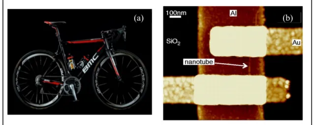
(a) (b)
Figure 2.5 (a) Bicycle made of CNT reinforced metal and, (b) AFM image of a CNT FET
minimal increase in weight percentage (Gojny et al. 2004). CNTs have also been used build lightweight turbines for windmills and hulls for naval boats.
CNT sheets have been demonstrated as materials for fuel cell electrodes and self-cleaning textiles (Lima et al. 2011). The addition of CNTs to metals has shown to increase the tensile strength and modulus. This can be used in aerospace and automobile applications.
It is well known that mechanical deformation can alter the electrical conductance of CNTs. This forms the basis for the application of CNTs in pressure sensing. A lot of works in the literature have been published about pressure and strain sensors based on CNTs. Electrical transition in SWNTs by radial deformation induced by hydrostatic pressure was studied using first principle calculations was studied by Wu et al. (Wu, Zang, et al. 2004). Kang et al. (Inpil et al. 2006) fabricated a CNT based strain sensor for applications in structural health monitoring. This work compared device performance between Buckypaper and a composite of SWCNT/Polymethylmethacrylate. A MWCNT based MEMS pressure sensor was developed and studied by Fung et al. (Fung et al. 2005) using dielectrophoresis to position the MWCNT network across a PMMA membrane. Deflection of the PMMA membrane under pressure induced bending in the MWNTs which was detected by fold electrodes with 3 µm to 10 µm spacing. This work uses conventional micromachining process without resorting to low throughput processes like electron beam lithography.
27
2.7 Carbon Nanotubes: Applications in MEMS and NEMS
CNTs have been extensively used to fabricate Nano and microscale resonators for applications in mass sensing. Jensen et al. (Jensen, Kim, and Zettl 2008) fabricated one of the most sensitive mass sensors using CNT as a resonator. The density of CNTs is lower than other materials fabricated by a similar method and thus the resonance frequency is lower which results in a larger magnitude of response at lower resonance frequencies, especially useful for sensing applications. The high carrier mobility in CNTs has been used to develop FETs. For example, CNT-FETs with conductance as high as the ballistic limit have been demonstrated previously with on/off ratios as high as 109 (Javey et al. 2003). The chirality and the metallic properties
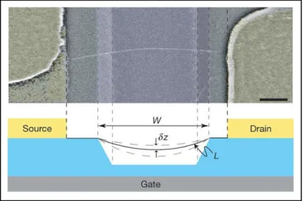
of CNTs highly influence the performance of the FETs. The metal contact to the FETs is also found to have a significant impact on the performance (Chen et al. 2005). Reproducibility for large scale applications remains a major challenge to overcome in this area since there is no process to produce CNTs with uniform electrical properties. Another example of such an application was a self-detecting nanotube resonator reported by Sazonova et al. (Sazonova et al. 2004) using the CNTs as transistors. The device design again consisted of an individual CNT suspended over a trench.
Figure 2.6 (Top) A false-colored SEM image of a suspended device and, (Bottom) Device geometry
Additionally, a gate electrode is used to induce an oscillatory motion using an AC voltage resulting in a resonant frequency of 55 MHz and a quality factor of 80. Upon subjecting the CNT to tension, a shift in the oscillation frequency was observed and thus the authors were able to tune the device to scale the resonant frequency from 3 to 200 MHz. The force sensitivity of the device was measured to be 1 fN/Hz-1/2 which is one of the best force sensitivities
determined to date. The authors predict that at temperatures of 1 kelvin, forces below 5 aN can be detected.
An important issue hindering the large-scale application of CNT FETs is that single CNT based devices can only be fabricated using e-beam lithography which is not feasible for large scale manufacturing. Many alternate methods have been proposed to overcome this challenge. For instance, highly aligned unipolar SWNTs grown by a CVD process have been demonstrated. The SWNTs are used as transistors with a conductance of 1000 cm2V-1s-1. Having an array of
highly aligned SWNTs improves the uniformity and reproducibility by reducing the role played by the chirality and defects in the SWNTs. However, determination of the number of active SWNTs during the FET operation remains an issue.
2.8 Carbon Nanotube Application Challenges
Even though the potential applications of CNTs are endless and there is an ever-growing interest in CNT research from thousands of researchers around the world, there are very few mass-produced products made from CNTs. One of the major challenges facing the commercial use of CNTs is cost. Even though the price of CNTs have reduced significantly in the past decade, the overall cost to manufacture CNTs on a large scale is still perceived to be too high. Another issue of concern is the growth and purity. To date, a technique to grow only a single species of CNTs with controlled chirality and diameter has not been developed fully, although techniques to sort nanotubes have certainly be developed (Janas 2018). Another issue is assembly. Billions of nanotubes are required for fabricating CNT based transistors or circuits. Manipulating billions of individual nanotubes is not an easy task and no techniques currently exist for doing so. However, with the speed of advancement in research, one can hope that it is only a matter of time that we can see CNTs in commercial applications such as sensors.
CHAPTER 3
GAS SENSING USING CARBON NANOTUBES Preface
The electrical and mechanical properties of CNTs have been studied and put to good use in many applications, especially sensing, as described in the previous chapter. One area of sensing that CNTs have been widely used is gas sensing. CNTs, both single and multiwalled, have been used successfully to detect gas concentrations as low as 1 ppb and gases such as Ammonia, Methane, CO2, etc. Many sensing principles such as change in capacitance,
resistance and thermal transfer mechanisms have been used in gas sensing applications. In the following chapter, a brief literature review of different gas sensors using CNTs as the sensing element is presented. Each reviewed work is then critically analyzed to determine the advantages and drawbacks of the as proposed device. In lieu of the theme of this Ph.D. work, a separate section about humidity sensing and humidity sensors is presented. A literature review for the common materials used for humidity sensing and a brief review about CNT based humidity sensors is presented.
Finally, a review of the CNT based ionization gas sensors is covered. The fabrication of an ionization sensor demonstrates the evolution of the device sensor. The discussion presents the working principle, advantages and disadvantages of ionization gas sensors.
3.1 Introduction
Gas sensors find widespread applications in space exploration, pharmaceutical industries and environmental monitoring. Sensors with high sensitivity and selectivity are of paramount importance to detect leakage of highly explosive gases such as hydrogen and other toxic gases such as methane. The basic criteria for a good gas sensor are:
1) Sensitivity, defined as the lowest concentration of the analyte that the sensor can detect, 2) Selectivity, defined as the ability of the sensor to detect a particular gas analyte in a mixture, 3) Fast response and recovery, defined as the time taken by the sensor to detect a minimum concentration of the analyte and recovery time is the time it takes for the sensor signal to return to its initial value after a step concentration change from a certain value to zero, 4) Long term stability.
The change in electrical properties of CNTs upon exposure to certain gases forms the basis of their application in gas sensing (Sinha, Ma, and Yeow 2006; Li et al. 2003).
31
3.2 Pristine Carbon Nanotube Gas Sensors
The presence of surface atoms on CNTs is ideal for the electrical detection of trace chemical elements. Two different configurations of CNT based gas sensors exist: chemiresistors and back-gated chemical field effect transistor (ChemFET).
In a chemiresistor configuration, CNTs are bridged between two electrodes. The analytes bind on the CNT surface resulting in charge transfer between the adsorbed molecule and the CNT surface resulting in change of electrical resistance. In the ChemFET configuration, the conductance of the CNT is modulated using a third gate electrode coupled by a thin dielectric layer. The ChemFET configuration is deemed a bit more sensitive than the Chemiresistor configuration due to the ability to tune the CNT conductance which makes them ideal candidates for electrical sensing, the downside being the requirement of complicated ancillary electronics.
Kong et al. (Kong et al. 2000) first demonstrated the use of semiconducting SWNTs can be used for gas sensing as ChemFETs. SWNTs were grown using Chemical Vapor Deposition (CVD) followed by patterning metal electrodes over individual SWNTs. The nanotubes
(a) (b)
Figure 3.1 (a) Response of SWNTs to NO2 and NH3 Taken from Kong et al. (2000) and,
(b) Device response of the ChemFET Sensor Taken from Novak et al. (2003)
showed good sensitivity to NO2 and NH3. The conductance of the CNTs increased by three
orders of magnitude when exposed to NO2 and decreased by two orders of magnitude when
exposed to NH3.
Novak et al. (Novak et al. 2003) also used CNTs in a chemFET configuration to detect dimethyl methylphosphonate (DMMP), a simulant for Sarin. The sensors demonstrated quick recovery on application of a gate voltage of 3 V. The fast desorption time was explained by Coulombic interaction, where application of a positive gate voltage induced a negative charge which interacted with DMMP, a strong electron donor and decreases the desorption barrier. For such applications, it is important for the CNT to have chemical selectivity against agents like water vapor. This has been addressed using polymers to filter out other vapors from air during testing. However, it remains to be seen how such a filtering system can be translated for commercial applications.
One of the potential drawbacks of using pristine nanotubes for gas sensing applications could be the lack of selectivity towards specific gaseous analytes and lack of sensitivity to species that do not interact with CNTs. This problem is solved by chemical functionalization.
There are two main types of functionalization possible: covalent and non-covalent functionalization. Most covalently functionalized CNTs are based either on amidation or esterification of carboxylic acid groups found on defect sites during acid treatment (Chen et al. 1998).
On the other hand, non-covalent functionalization is based on forces such as Van der Waal’s interactions and π – interactions without actually influencing the physical properties of the CNTs (Star et al. 2001). A Carbon monoxide (CO) sensor using SWNTs modified with thiolated heme (Dong et al. 2007) was fabricated in a ChemFET configuration. The sensor exhibited greater sensitivity to CO when contacted with Cr than Au showing that the CNT-metal interface is an important factor for determining sensor performance. The sensor had a response time of less than 100 s with a detection limit of 4.9 ppm. One potential drawback of this work is the repeatability. The authors report that the sensors perform optimally for 40 cycles after which there is a performance degradation. This can be a problem for long term applications.
33
CNT-polymer nanocomposites are also promising hybrid materials for use in gas sensing. For example, An et al. fabricated a polymer-CNT sensor for NO2 sensing (An et al. 2004). A
uniform film of polypyrrole on the surface of SWNT was achieved by in-situ chemical polymerization. The sensitivity of the SWNT-Polymer hybrid was 10x higher than the polymer alone. SWNTs functionalized with poly-(m-aminobenzene sulfonic acid) (PABS) were shown to have better sensitivity to NH3 than simple carboxylated SWNTs (Zhao, Hu, and Haddon
2004). The better sensitivity was attributed to the protonation and deprotonation of the PABS which altered the charge carrier density in the SWNTs.
A multifunctional chemical sensor based on CNTs that are vertically aligned was fabricated (Wei et al. 2006). The vertically aligned CNTs were coated with different polymers. The sensor showed fast and reversible sensing of volatile organic solvents (VOCs).
The sensing mechanism was explained based on charge transfer interaction with the gas molecules and the change in inter-tube distance due to polymer swelling during gas adsorption.
3.3 Suspended Carbon Nanotubes for Gas Sensing
In the previous section, a survey about CNT based gas sensors was discussed. Here, a review (b)
(a)
Figure 3.2 (a) Hysteresis free operation of a suspended NO2 gas sensor fabricated
Taken from Chikkadi et al. (2013) and,
(b) SEM micrograph of an individual suspended MWCNT acting as an electrothermal gas sensor Taken from Kawano et al. (2007)