HAL Id: tel-00697615
https://tel.archives-ouvertes.fr/tel-00697615
Submitted on 15 May 2012HAL is a multi-disciplinary open access
archive for the deposit and dissemination of sci-entific research documents, whether they are pub-lished or not. The documents may come from teaching and research institutions in France or abroad, or from public or private research centers.
L’archive ouverte pluridisciplinaire HAL, est destinée au dépôt et à la diffusion de documents scientifiques de niveau recherche, publiés ou non, émanant des établissements d’enseignement et de recherche français ou étrangers, des laboratoires publics ou privés.
Realization of ultrathin Copper Indium Gallium
Di-selenide (CIGSe) solar cells
Zacharie Jehl
To cite this version:
Zacharie Jehl. Realization of ultrathin Copper Indium Gallium Di-selenide (CIGSe) solar cells. Other [cond-mat.other]. Université Paris Sud - Paris XI, 2012. English. �NNT : 2012PA112058�. �tel-00697615�
Thèse de doctorat de l’Université Paris Sud-Orsay (Paris XI)
ED MIPEGE - Modélisation et Instrumentation en Physique, Energies, Géosciences et Environnement
Présentée par
Zacharie Jehl Li Kao
pour l’obtention du grade de docteur de l’Université Paris XI
Elaboration of ultrathin Copper Indium Gallium
Di-Selenide based Solar Cells
Présenté, le 4 avril 2012 devant le jury composé de : Abdelilah Slaoui Rapporteur
Nicolas Barreau Rapporteur Michael Powalla Examinateur Marc Burgelman Examinateur Isabelle Gérard Examinatrice Jean-Paul Kleider Président
Negar Naghavi Co-Directrice de thèse Daniel Lincot Directeur de thèse
Acknowledgements
The making of this thesis would not have been possible without Dr. Daniel Lincot, my PhD director. I am grateful for his remarkable scientific culture, his innovative ideas and his ability to express complicated concepts with simple sentences. I am thankful to Dr. Negar Naghavi, coordinator of the UltraCis project and co-director of this study. She supported me and encouraged me during the harsh times that every PhD student goes through. Her knowledge of alternative buffer layers was precious, and she spent hours and hours to review my articles and this thesis.
I wish to thank Dr. Abdelilah Slaoui and Dr. Nicolas Barreau for accepting to review this thesis. I know that they both are very busy scientists with many responsibilities and i really appreciate that they took time working on this thesis. I am also very happy that Dr. Michael Powalla could join the jury. Having such renowned person in the jury is an honor. Similarly, it is a real honor that Dr. Marc Burgelman is part of the jury. I worked for three years using the software that he and his team designed, and so I am thankful both for his presence, and his indirect scientific contribution. I gratefully thank Dr. Jean Paul Kleider for being part of the jury; his expertise in the field of electrical characterizations is precious to bring new insights on this thesis. And finally, I am more than thankful to Dr. Isabelle Gérard both for being part of this thesis jury, and for her work during the UltraCis project. She taught me the CIGSe etching technique, without which this thesis would not even exist. I also acknowledge Dr. Jean-François Guillemoles, for his advices, explanations, and general scientific contribution to this study. I particularly appreciated his availability and constant good mood. I am more than thankful to Dr. Felix Erfurth who was a post-doc at IRDEP for one year, and worked in close collaboration with me. His scientific qualities, hard work, and enthusiasm led us to significant breakthrough.
I would like to thank all the partners involved in the UltraCis project: “Institut Lavoisier de Versailles”, “Laboratoire de Photonique et Nanostructures”, “Laboratoire de Génie Electrique de Paris”, “Würth Solar/ZSW”, and last but not least, the “Laboratoire Charles Fabry” of “Institut d'Optique”; thank to their work, original ideas and collaboration with us, we were able to move forward with this project. I particularly thank Dr. Nir Dahan from “Institut d'Optique” who I worked with for the past two years. I appreciate you both as a scientific and as a person. I also acknowledge Dr. Jean Rousset from IRDEP, who worked with me in the
beginning of this thesis on the Zinc Oxide nanorods subject. I really had a great time with you.
Je remercie toute les personnes que j'ai pu côtoyer à l'IRDEP ces trois dernières années et tout particulièrement Arthur Lebris, inventeur de la contrepèterie la plus drôle depuis celle du Fakir, Frédérique Donsanti, dont l'aide fut précieuse dans les labos et la compagnie agréable à l'extérieur, Marie Jubault, ma "voisine d'en face" avec qui j'ai pu partager ma passion de la Nu-Soul, Myriam Paire, qui ne sait toujours pas calculer un pH, Jacqueline Destombes, dont la patience à mon égard concernant toutes les démarches administratives force le respect, et enfin Servane Haller, pour tant de choses que je n’aurais pas assez de ces 270 pages.
J'ai la chance d'avoir une famille qui s'est toujours souciée de moi, et je les remercie pour tout car ils sont à n'en pas douter la meilleur part de moi même. Merci à mes Grands Parents, merci à mon Frère, merci à mon Père et à ma Mère, et bien sur à tout(e) mes Cousin(e)s (Thierno, Simon, Nastunia, Jess…), Oncles, Tantes. J'ai une pensée toute particulière pour ma grand mère J. Li-Kao qui hélas n'aura pas vu cette thèse s'achever.
Mes amis sont tous une part très importante de ma vie et leur présence, certains depuis plus de 23 ans, m'a sans aucun doute apportée la stabilité et l'équilibre nécessaire pour achever mes études. Pape aka « Man of Stile », Sadat aka « Mâle Alpha», Menad aka « Le meilleur d'entre nous », Bren-ya aka « Bren de la P-loche », François aka « Freaka », Benjamin aka « casse toi que je mate mon Berserk », Jeff aka « Swagg-man », Harry aka « la Suisse », Hervé aka « Kyano_Thunderfury », Oumar aka « le mec balaise », André aka « B3NTO », Lev aka « le mec qui jette des pizzas par la fenêtre », Gihan aka « le futur marié », Habib aka « Satan », Baptiste aka « le dragueur de la tour C », ainsi que tout ceux que je n’ai pas la place de citer (Maxime, Christophe, Jean-Jacques etc. je vous ai pas oublié!). Merci, pour tout, et pour le reste. Je remercie également Bernard et Jean-Christophe, mes voisins profs! Et enfin, je remercie Wilaï, pour tout.
GENERAL INTRODUCTION 9
MOTIVATION 9
SCIENTIFIC APPROACH 10
CHAPTER I: 13
STATE OF THE ART 13
I) THE COPPER INDIUM GALLIUM DISELENIDE (CU(IN,GA)SE2) SOLAR CELL 14
II) STATE OF THE ART IN THINNING OF CIGSE ABSORBER 19
CHAPTER II 27
THEORETICAL ANALYSIS: EFFECT OF THINNING OF CIGSE ABSORBER LAYERS ON SOLAR CELLS CHARACTERISTICS AND POTENTIAL
IMPROVEMENTS FOR ULTRATHIN DEVICES 27
II.1) INTRODUCTION 28
II.2) MODELING OF A STANDARD CIGSE SOLAR CELL 29
II.2.A) DEFINITION OF THE INPUT PARAMETERS 29
II.2.B) MODELING OF CURRENT-VOLTAGE AND SPECTRAL RESPONSE 33
II.3) INFLUENCE OF CIGSE THICKNESS ON PHOTOVOLTAIC PARAMETERS 35
II.3.A) MODELING OF THE CURRENT-VOLTAGE CURVES 35
II.3.B) MODELING OF SPECTRAL RESPONSES 40
II.3.C) CONCLUSION 43
II.4) ANALYSIS OF POTENTIAL IMPROVEMENTS FOR ULTRATHIN CIGSE SOLAR CELLS 45
II.4.A) INTRODUCTION 45
II.4.B) FRONT AND BACK SIDE OPTICAL ENGINEERING FOR EFFICIENT LIGHT MANAGEMENT 45
II.4.C) REDUCTION OF THE BACK CONTACT RECOMBINATION BY ENERGY BAND ENGINEERING 49
II.4.D) POTENTIAL IMPROVEMENTS FOR AN ULTRATHIN 100 NM CIGSE SOLAR CELL 58
CHAPTER III 67 EXPERIMENTAL RESULTS ON CHEMICALLY ETCHED THIN OF CIGSE
ABSORBERS LAYER; SOLAR CELLS ELABORATION AND
CHARACTERIZATIONS 67
III.1) INTRODUCTION 68
III.2) STATE OF THE ART IN THINNING OF CIGSE ABSORBERS 69
III.3) CHEMICAL ETCHING OF CIGSE 76
III.3.A) EXPERIMENTAL SETUP 76
III.3.B) RESULTS 77
III.4) CHARACTERIZATION OF ETCHED CIGSE FILMS 82
III.4.A) MATERIAL CHARACTERIZATION 82
III.4.B) OPTICAL CHARACTERIZATION OF ETCHED CIGSE FILMS AND SOLAR CELLS BY
SPECTROSCOPIC REFLECTIVITY AND PHOTOLUMINESCENCE 94
III.5) ELECTRICAL CHARACTERIZATION OF CIGSE SOLAR CELLS WITH ABSORBER THINNED
BY CHEMICAL ETCHING 101
III.5.A) EXPERIMENTAL SETUP 101
III.5.B) CURRENT-VOLTAGE CHARACTERIZATION 102
III.5.C) SPECTRAL RESPONSE 106
III.5.D) CONCLUSION 110
III.6) INFLUENCE OF THE SURFACE ROUGHNESS ON THE CIGSE SOLAR CELLS 111
III.6.A) DEVICE CHARACTERIZATION 111
III.6.B) DISCUSSION 115
III.6.C) ANALYTICAL EXPRESSION OF THE SPECTRAL RESPONSE 118
III.6.D) CONCLUSION 122
III.7) CHAPTER CONCLUSION 124
CHAPTER IV 127
FRONT CONTACT ENGINEERING OF THIN CIGSE SOLAR CELLS 127
IV.1) INTRODUCTION 128
IV.2.A) ANTI-REFLECTING COATING LAYERS 130
IV.2.B) LIGHT SCATTERING EFFECT BY TEXTURATION OF THE FRONT ZNO:AL WINDOW 132
IV.2.C) ALTERNATIVE ZNS/(ZN,MG)O BUFFER LAYER FOR CIGSE SOLAR CELLS 142
IV.2.D) CONCLUSION 144
IV.3) EXPERIMENTAL RESULTS 145
IV.3.A) LIGHT SCATTERING AND ANTIREFLECTION EFFECT FOR ULTRATHIN CIGSE SOLAR CELLS BY ZNO:AL CHEMICAL TEXTURATION AND ELECTRODEPOSITION OF ZNO NANORODS 145 IV.3.B) COMPARATIVE STUDY BETWEEN STANDARD CDS AND ALTERNATIVE ZNS BUFFER LAYERS ON CHEMICALLY THINNED CIGSE ABSORBER SOLAR CELLS 164
IV.4) CHAPTER CONCLUSION 169
CHAPTER V 171
BACK CONTACT ENGINEERING FOR THIN AND ULTRATHIN ABSORBER
CIGSE SOLAR CELLS 171
V.1) INTRODUCTION 172
V.2) STATE OF THE ART 174
V.2.A) METALLIC BACK CONTACT 174
V.2.B) TRANSPARENT BACK CONTACT 181
V.2.B) CONCLUSION 184
V.3) METALLIC BACK CONTACT 185
V.3.A) INTRODUCTION 185
V.3.B) EXPERIMENTAL 185
V.3.C) CHEMICAL ANALYSIS OF THE MO/CIGSE BACK CONTACT INTERFACE 188
V.3.D) OPTICAL CHARACTERIZATION OF THE MO/CIGSE INTERFACE AND ALTERNATIVE BACK
CONTACT INTERFACE 191
V.3.E) ELECTRICAL CHARACTERIZATION BY TRANSMISSION LINE MEASUREMENTS OF THE METAL/CIGSE INTERFACE FOR DIFFERENT METALS 194 V.3.F) ELECTRICAL CHARACTERIZATION OF THIN ABSORBER SOLAR CELLS WITH AU BACK CONTACT AND COMPARATIVE STUDY WITH STANDARD MO BACK CONTACT 199
V.3.G) CONCLUSION 207
V.4) TRANSPARENT BACK CONTACT BASED ON ZNO:AL 208
V.4.B) ELECTRODEPOSITED THIN CU LAYER AT THE CIGSE/ZNO:AL INTERFACE 210
V.4.C) ELECTRODEPOSITED CU2O INTERFACIAL BUFFER LAYER 216
V.5) ULTRATHIN CIGSE SOLAR CELL WITH LAMBERTIAN LIGHT SCATTERING BACK
REFLECTOR 220
V.5.A) OPTICAL SIMULATION OF A 100 NM CIGSE SLAB WITH LAMBERTIAN BACK REFLECTION
221 V.5.B) LIGHT ABSORPTION IN AN ULTRATHIN 200 NM CIGSE SOLAR CELL STRUCTURE 223
V.5.C) CONCLUSION 228
V.6) CHAPTER CONCLUSION 229
GENERAL CONCLUSION AND PERSPECTIVES 233
REFERENCES 241
APPENDIX 253
I) MODELING PARAMETERS OF THE REFERENCE SOLAR CELL 253
II) CHARACTERIZATION TOOLS 260
SCANNING ELECTRON MICROSCOPY (SEM) 260
ATOMIC FORCE MICROSCOPY (AFM) 260
X-RAY PHOTOELECTRON SPECTROSCOPY 261
ELECTRICAL CHARACTERIZATION 262
III) STATE OF THE ART INSIGHTS FOR ZNS/(ZN,MGO) DEPOSITION 264 IV) OPTICAL SIMULATION OF A SOLAR CELL STACK USING THE RADIATIVE TRANSFER
General Introduction
Motivation
Copper indium gallium diselenide (CuIn1-xGaxSe2 or CIGSe) solar cells present the highest
conversion efficiency ever reported in thin film technology, with a record value of 20.3% recently reported by ZSW 1. Over the past decade, the CIGSe field experienced an increasing industrial development with the commercialization of high efficiency modules 2. It is now considered as one of the most promising alternative technology to silicon-based solar cells, and to meet the production milestone of 0.5 $ per watt for cost parity with other energy sources. In the scope of increasing the development of the CIGSe technology up to the Giga-Watt, the issue of possible material scarcity arises. While copper and selenium are abundant materials, gallium and more importantly indium are limited resources, and their availability may become a problem for future development of CIGSe-based solar cell 3; moreover, indium is already a widely used material for indium tin oxide (ITO) production which is strongly related to the overwhelming flat screen industry. Therefore, the future of the CIGSe technology seems closely tied with the question of materials savings.
In this scope, several alternatives have been proposed in the recent years, such as replacing In and Ga by more abundant materials such a Zn and Sn (kesterite material). Although recent improvements have been achieved (with efficiencies up to about 11% 4), the efficiency of these solar cells is still 2 times lower than record CIGSe solar cells. Another idea to reduce the material utilization in CIGSe solar cells is to reduce their dimensions, either by reducing the lateral dimensions 5 of the device, or the thickness of the device. In recent review 3, V. Fthenakis suggested that an extensive R&D is needed on developing thinner layers, which has not been sufficiently studied so far.
In this PhD thesis, we will focus on developing CIGSe solar cells with very thin and ultrathin absorber layers, down to 100-200 nm, while the standard thickness of CIGSe layers is 2500 nm. Besides using 25 times less indium in the fabrication of a solar cell, such an achievement will markedly reduce the deposition time of the material, and thus significantly increase the throughput of the process and the machinery utilization, leading major cost reduction.
However, the competitiveness of the CIGSe material relies on its high efficiency compared to other thin film technologies; therefore, the reduction of the CIGSe absorber thickness must not be linked to an efficiency decrease of the solar cell. It is thereby necessary to develop innovative theoretical and experimental designs that could allow to maintain the efficiency of ultrathin absorber solar cells at the same level as the current thick absorber solar cells. The main objective of our researches is to propose new front contact and back contact engineering on ultrathin absorber solar cells, to overcome the various efficiency limitations that exists when reducing the CIGSe thickness in a solar cell. For that, we will propose a novel approach combining chemical etching of the absorber, and low temperature back contact processing.
Scientific approach
In the first Chapter of this thesis, we will introduce the general state of the art of thinning the CIGSe absorber for very thin and ultrathin solar cells, with a short overview of the available literature on this subject. In a second Chapter, we will study from a theoretical point of view the effect of reducing the absorber thickness in a CIGSe solar cell by using numerical tools (SCAPS, and optical simulation ). New solution to increase the performances of the very thin and ultrathin absorber CIGSe solar cells will be proposed, and theoretically evaluated. In the third Chapter of this thesis, we will experimentally reduce the CIGSe thickness using a chemical bath etching based on a bromine solution. The resulting CIGSe films will be characterized by various tools in order to evaluate the chemistry, the crystallinity, the composition and the optical properties of the etched CIGSe films. Solar cells with very thin and ultrathin absorber thickness down to 200 nm will be realized and electrically characterized, in order to compare the experimental photovoltaic parameters with our simulations. In Chapter IV, we will investigate on the front contact engineering to improve the light absorption of very thin absorber CIGSe solar cell. Various solutions will be tested, including the introduction of new materials in the stack and nanostructuration of layers. In the final Chapter (V), we will study the back interface engineering of very thin and ultrathin absorber CIGSe solar cell. We will propose an innovative methodology for the replacement of the back contact of the CIGSe solar cell by alternative materials and structures, and demonstrate the feasibility of high efficiency ultrathin devices with proof of concept devices. At the beginning of each chapter, a specific state of the art of the current literature on the topic will be presented, in complement of the short overview from Chapter I.
Chapter I:
I) The Copper Indium Gallium DiSelenide (Cu(In,Ga)Se
2)
solar cell
Copper indium gallium diselenide (CuIn1-xGaxSe2 or CIGSe) solar cells is a multi layer thin
film technology which has been increasingly developed in the last decade thanks to its relatively low cost combined with high efficiencies 1,6. CIGSe is a direct bandgap semiconductor with a chalcopyrite structure, a p-type doping and a bandgap varying continuously with the gallium content x from about 1 eV (for pure CuInSe2) to about 1.7 eV
(for pure CuGaSe2). Thanks to the very high absorption coefficient of more than 105.cm-1 for
1.5 eV and higher energy photons 7, CIGSe solar cells require a much thinner film (~2 µm) than most of the other semiconducting materials. Although alternative plastic or metallic substrate can be used 8,9, we focus in this work on the study of CIGSe solar cells deposited on soda lime glass (SLG) which is both the most widely used substrate and the one giving the best efficiencies. The solar cell stack is presented figure 1. A Mo layer is deposited on the glass substrate by sputtering with a thickness of about 500 nm. This layer is the back contact of the solar cell. Mo has been chosen because of its excellent chemical compatibility with CIGSe (no interdiffusion of the species throughout the absorber during thermal stress) and its ability to form an ohmic contact with the CIGSe, because of the presence of a thin MoSe2
layer at the interface between the two materials 10–13. The p-CIGSe layer can be grown by several vacuum and non vacuum methods, such as co-evaporation 1,6, sputtering 14,15, electrodeposition 16,17 or nano-particles based techniques 18; in this work, we focus on the study of a 2.5 µm CIGSe layer deposited by co-evaporation using an industrial three stages process described in reference 2. This process allows to obtain high efficiencies along with a very good reproducibility. A n-doped buffer layer is deposited on top of the absorber; the most widely used is chemical bath deposited cadmium sulfide (CdS) 19 with a bandgap of 2.4 eV and a thickness of 50 nm. This layer allows the formation of the p-n junction with the CIGSe and passivates the absorber surface which strongly reduces recombination at the p-n interface. The band offset of the CdS on CIGSe is particularly suitable for the following ZnO:i/ZnO:Al bi-layer. However, the relatively low bandgap of this material has been highlighted as a major issue to overcome for increasing the photon absorption in the CIGSe. Cd toxicity is also pointed out as a reason for replacing this buffer layer by an alternative buffer. The top zinc oxide bi-layer is deposited by sputtering as a transparent front contact for
the solar cell. The thin (between 50 and 70 nm) intrinsic n-doped ZnO:i layer (IZO) provides an efficient isolation of potential small shunt conductance, along with protecting the CIGSe/CdS interface from the rest of the process. Degenerate n-doped ZnO:Al (AZO) with a thickness of about 400 nm is the most commonly used transparent conducting oxide in the CIGSe field, and act as a transparent front contact.
The band diagram of the complete solar cell under illumination is presented in figure 2. We see that the p-n junction between p-CIGSe and n-CdS/ZnO creates a space charge region which extends in the region of the structure, due to the much lower doping level of the p-region compared to the n-p-region. The difference in the work function between the p and the n materials creates a built-in potential VBI. Incident light passes through the wide gap
ZnO:i/ZnO:Al (Eg =3.3ev−3.5eV) front window, and through the CdS buffer layer (Eg =2.4eV) where high energy photons are partly absorbed but do not contribute to the photocurrent output. When the photons reach the CIGSe absorber, they are absorbed in the material, which separates the holes and the electrons by exciting them in the conduction band. This increases the density of electrons and holes above their equilibrium values leading to a splitting of the quasi Fermi levels (i.e. a difference in the chemical potential of electrons and holes). Migration of the electrons from the p-doped region to the n-doped region creates a minority carriers current, and the electrons are collected at the ZnO:Al front contact while the hole reach the metallic back contact.
Figure 1. Material stack of a standard CIGSe solar cell
Figure 2. Band diagram of a standard CIGSe solar cell with no polarization and under
The quasi fermi level splitting drives the maximum value of the Open-Circuit Voltage (Voc) of
the solar cell. The short circuit current (Jsc) is defined as the current delivered by the cell at 0
voltage. When the diode is polarized in direct, the maximum power output Pm =Vm.Jm is reached, also called the operating point, for a voltage Vm <Voc and a current Jm < Jsc. The Fill Factor FF is defined as
sc oc m m J V J V FF . .
= . The efficiency η of the solar cell is the ratio between the maximum power output P and the incident power m P . Under standard A.M. 1.5 s
solar radiation, Ps =1000W.m−2. Therefore, in standard conditions, we have 1000 . . 1000 .J V J FF Vm m = oc sc =
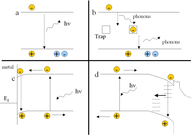
η . Several factors may limit the solar cell efficiency; the most important ones are shunt resistance arising from leakage of current through the cell, series resistance coming from each layer composing the solar cell and the interfaces between the layers, and carrier recombination that may occurs in the stack. The main recombination processes in solar cells are schematized figure 3. The band to band recombination process is basically the inverse process of the electron-hole pair generation from light absorption in the material (Figure 3.a). An electron from the conduction band falls back to the valence band and releases its energy in the form of a photon hν . Another very important recombination process is the recombination by phonon emission (Figure 3.b), also called Shockley-Read-Hall (SRH) recombination. This type of recombination is trap-assisted utilizing a defect at the energy Et
within the material bandgap Eg. The excess energy during the recombination of the carrier is
transferred to the crystal lattice by phonons. The theory describing this effect can be found in references 20,21. Interfaces, because of their higher defect density, are often region of high SRH recombinations. Back contact recombination (Figure 3.c), occurring when electron reach the metallic back contact, are often neglected for standard CIGSe solar cell due to the important thickness of the absorber. However, their influence becomes of major importance for thinner absorber layer, particularly for low energy photons that are absorbed deeper in the CIGSe, and thus closer to the back contact. Finally, recombination at the CIGSe/CdS interface which could be assisted by tunneling can also occur, due to interface defects (Figure 3.d).
Figure 3. Schematic representation of the major recombination processes in a CIGSe solar
cell. (a) radiative band-to-band; (b) Shockley-Read-Hall; (c) back contact; (d) interface recombination with possible tunneling
When reducing the absorber thickness, the device becomes more sensitive to various parameters such as the material absorption, the increased recombination etc… In the following, we will expose a general overview of previous studies related to thinning the CIGSe absorber, which will give us leads to follow throughout our experiments.
II) State of the art in thinning of CIGSe absorber
Since reducing the absorber thickness in CIGSe solar cell has been pointed out as a key issue in this sector, several groups have tackled the task both from a theoretical and experimental points of view and designed devices with thinner absorbers. Systematic study of the reduction of the absorber thickness was first reported by Shafarman et al. in 1997 22 and Negami et al. in 1998 23. Since then, the most active groups have been the NREL group 242526 and the Uppsala University group 27 28 with extensive studies on this topic. Those two groups proposed the same approach for reducing the absorber thickness, consisting in directly growing the CIGSe layer at a lower level, thus adapting the existing process to a lower thickness.
When reducing the absorber thickness of a photovoltaic device, the most expected problem is the reduction of the light absorption and so the decrease of the photocurrent generation in the solar cell. Although the absorption coefficient of the CIGSe material is very high, all the studies have shown that the amount of light absorbed is strongly affected when decreasing the absorber thickness to the sub-micrometer level. Moreover, other problems may appear due to the ultra-low scale of the devices. Negami 23 reported that the solar cells were electrically shunted when the absorber thickness became close to 0.5 µm; this was related to the natural roughness of as-grown CIGSe layers which was of the same order as the film thickness itself. Shafarman et al. 22 also reported a strong decrease of the parallel resistance when reducing the CIGSe thickness, most likely related to an increased shunt effect due to pinholes in the absorber. However, Karpov et al. predicted, in a theoretical simulation study, the existence of a critical device thickness in the submicron region, below which the leakage currents will harm the device performance 29. Gloeckler and Sites 30 also investigated on the properties of very thin and ultrathin absorber CIGSe solar cells from a theoretical point of view. Their simulations indicated that reducing the absorber thickness leads to a reduction of the short circuit current due to a combination of a reduced light absorption and increased back contact recombination. When the absorber is fully depleted however (thickness lower than the space charge region width), the authors state that the back contact recombination become negligible and the current of the cell depends only on the absorption in the CIGSe.
The Uppsala group’s first publication 27 on the topic used a Cu-poor fabrication process giving a relatively smooth surface (RMS ~ 40 nm), which strongly reduces the risk of shunting for thin CIGSe absorbers. However, a much smaller grain size is achieved when compared to a classical three stage process. In this study, a 1.8 µm solar cell with an efficiency of about 16 %, a Fill Factor (FF) of 75 % and an Open Circuit Voltage (Voc) of 650
mV is taken as a reference thick absorber solar cell, and solar cells with thinner absorbers are realized using the same process, down to 0.15 µm. Efficiencies close to 13 % are achieved down to 0.8 µm, showing a moderate decrease when reducing the absorber thickness; however a more pronounced decrease is observed for the lower thicknesses down to 8 % for a 0.36 µm absorber solar cell. The results indicate that the dominant loss is seen in short circuit current. External Quantum Efficiency (EQE) and absorption measurements are performed on the devices (figure 4), showing that the light absorption is only slightly reduced when decreasing the absorber thickness from 1.8 µm to 0.8 µm; the EQE was however strongly affected in the long wavelength range. This reduced carrier collection for low energy photons is interpreted to an increased back contact recombination, thus confirming the simulations from Gloeckler & Sites 30. For the ultrathin 0.36 µm device, the absorbed light was strongly reduced compared to a thick CIGSe layer in the red and infrared range. Moreover, the difference between absorbed light and collected carriers is even more important and a high fraction of the generated carrier do not contribute to the current. On the other hand, the Voc
and the FF are essentially not affected down to ~0.5 µm absorber thickness, maintaining high values close to 650 mV and 73 % respectively. At the ultrathin scale however (d < 0.4 µm), the Voc and the FF are reduced although still at relatively high values (600 mV and 70 % respectively).
Figure 4. Comparison between the calculated absorption curves (solid) and the corresponding
QE curves (dotted) for CIGS thicknesses of 1.8, 0.8 and 0.36 µm 27
This paper also studies the influence of a back surface field (BSF) on the devices created by inserting a CuGaSe2 layer. It has been shown that by using graded compositional profiles, i.e.
increasing the Ga content at the back side of the solar cell, the conduction band level in the CIGSe increases 31. This leads to a reduced back contact recombination as reported in reference 32. With the introduction of this layer, the FF increases above 75 % while the Voc is
increased by about 30 mV, whatever the CIGSe thickness. The short circuit current however, which is the dominant loss responsible of the efficiency drop, is not improved by the introduction of the BSF. Diode analysis using a 1-diode model with dark and illuminated J-V measurements revealed that reducing the absorber thickness leads to a gradual increase of the saturation current J0, which is governed by the recombination processes, and an increase of
the diode ideality factor A. This is interpreted as related to the reduction of the Voc of thinner
absorber devices, while the reduction of the FF is accounted to the increase of J0 and a
decrease of the shunt resistance Rsh. The authors attribute the increase of the saturation current
to a combination of different phenomena; firstly, thinner absorber increases the back contact recombination and thus reduces the carrier collection. The fact that the FF is improved by the back CGSe layer is an indication that some loss mechanism can be reduced with a BSF, but the losses observed in the EQE curves remain however unchanged with the BSF. The thinner CIGSe layers also have smaller grain and thus larger grain boundaries than thick layers, which
could also account for the increased recombination losses. Finally, according to reference 33, the fact that the EQE of the 360 nm absorber solar is reduced in the short wavelength range combined with an increased ideality factor indicates tunneling recombination in the region close to the CIGSe/CdS interface.
Ramanathan et al. 24 investigated the influence of the thermal evaporation growth process on 1 µm thick CIGSe solar cells; they compare a three stage process with simultaneous co-evaporation of all the elements in one step. The three stage process consists here in the deposition of a (In, Ga)2Se3 layer, then reacted with Cu and Se. The composition is controlled
by detecting the temperature change of the substrate during Cu-poor to Cu-rich transition at the end of the second stage. The third stage is the evaporation of In and Ga in the presence of Se. The reduction of the CIGSe thickness in the three stage process is achieved by reducing the thickness of the precursor film in the first stage. On the other hand, several co-depositions were made, starting with a Cu-rich CIGSe layer or a CuGaSe2 layer, and the flux were
adapted to obtain films with the desired element ratio.
These different methods were successfully adopted to deposit absorbers in the thickness range of 0.4-1 µm and a bandgap grading was achieved in all the scenarios. Table 1 presents the best solar cell results as a function of the absorber thickness. A reference thick absorber solar cell is also presented.
Figure 5. External Quantum Efficiency for a thin 1000 nm CIGSe solar cell (solid line) and
thick 2500 nm CIGSe solar cell (dotted line) 24
The highest efficiency for a 1 µm CIGSe solar cell was achieved for a three stage process absorber with 17.1 %. When comparing the EQE of this solar cell with the thick 2.5 µm solar cell (figure 5), they notice that the long wavelength energy edge is at higher energy for the thin absorber, which is an indication of a higher Ga content. The Voc is however lower than
expected in this configuration by about 50 mV, which is the most significant loss that contribute to the difference in the efficiency between a thin and a thick absorber solar cell as seen on table 1. Dark J-V curves analysis shows that while the diode ideality factors are identical between a thin and a thick solar cell, the reverse saturation current is slightly higher in the case of a thin absorber (8.10-11A.cm-2 versus 3.10-11A.cm-2) which partly explains the decrease in Voc observed for thin absorbers. Drive-level capacitance profiling (DLCP)
measurements were performed on three stage absorbers with different thicknesses in order to evaluate their free carrier and defect density. This characterization reveals an increasing trend in both the carrier and defect density when decreasing the absorber thickness. The increase in the free carrier density does not results in an increase of the Voc due to the counter effect of
the increasing defect density. This is attributed to a non-optimum growth of the thinner CIGSe layers.
Instead of directly growing the absorber to a thinner scale, which may lead to the problems previously reported, more fundamental studies can be performed by reducing the thickness of a standard absorber by chemical etching. The chemical etching of CIGSe surface was first introduced by Birkmire and McCandless in 1988 34, who realized specular CIGSe surface
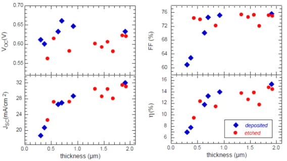
with this technique. This paper was followed by a publication from Canava et al. who reported a method to reconstruct the surface termination of CIGSe after etching by using a KCN post treatment 35. Based on these results, Shafarman’s team also investigated the etching of CIGSe films, but for reducing the absorber thickness 36. They performed a systematic comparative study between etched absorbers and as-deposited absorbers of the influence of reducing the CIGSe thickness on the photovoltaic parameters of the solar cells (Figure 6). They reported a similar trend for the Jsc when etching absorber as what was observed for
as-deposited CIGSe, with a progressive decrease due to the reduction of the thickness of the active material. However, in the case of etched absorbers the FF is found much more stable when reducing the CIGSe thickness than for as-deposited absorbers. On the other hand, the Voc of etched absorber solar cells is reported as slightly lower although the important dispersion of the results makes it difficult to interpret. Overall, the efficiency trend and value is identical between etched and as-deposited absorbers.
Figure 6. Compared photovoltaic parameters for CIGSe solar cells with different absorber
thicknesses realized with two different techniques: direct deposition of the absorber (blue dots), and chemical etching of thick absorbers (red dots) 36
In this Chapter, we had an overview of the general literature on CIGSe solar cells with thinned absorber. When reducing the CIGSe thickness, the short circuit current has been identified as the dominant loss in the solar cell. This has been attributed to a contribution of both incomplete absorption of incident photons due to the thinning of the absorber, and increased back contact recombination due to the increased proximity of the back interface for thin CIGSe layers. Open Circuit Voltage and Fill Factor are also affected although in much lower proportions, especially for very thin CIGSe absorber (less than 500 nm).
In this work, our goal is to study the feasibility of very thin and ultrathin absorber device with photovoltaic properties comparable to standard thick absorber solar cells. In the following Chapter, we will firstly study the influence of reducing the absorber thickness in a state of the art CIGSe solar cell by numerical simulation. We will try to investigate the physical factors that are involved in the decrease of the performances of the device, in order to address new and adapted techniques to significantly enhance the photovoltaic parameters of very thin (down to 400 nm) and ultrathin (down to 100 nm) absorber CIGSe solar cells. These materials and structures will be implemented in a numerical modeling to evaluate their potential in the scope of future application to experimental proof of concept devices.
Chapter II
Theoretical Analysis: Effect of thinning of
CIGSe absorber layers on solar cells
characteristics and potential improvements
for ultrathin devices
II.1) Introduction
As presented in the previous chapter, thin film solar cells and especially chalcogenide thin film solar cells have been extensively studied in the last three decades, and significant advances have been achieved leading to an increasing development of this technology. We however pointed out that although the current material cost is only a small fraction of the total solar panel cost, this rising evolution may lead to a major increase of the material price (both for CIGSe and CdTe) in a near future 3 37, and the limited material resources (for In and Te) may become an important limitation to upcoming developments of the sector. In order to limit the bottleneck due to the availability of the material, recent researches have been carried out to reduce the material consumption by thinning the absorber layer, both in CdTe 37 38 39 and CIGSe 22 23 24 27; this is the topic of our present study. In order to evaluate the influence of reducing the absorber thickness in a CIGSe solar cell, it is important at first to perform numerical simulations of very thin and ultrathin absorber solar cells, and to establish interpretations and hypothesis that will give us a trail to follow in the experiments.
In this Chapter, we focus on modeling a standard CIGSe solar cell using SCAPS 2.904, that will be used as a baseline. We will then study the influence of progressively reducing the CIGSe absorber thickness down to 100 nm. SCAPS is a worldwide recognized simulation software created by Prof. Burgelman from the University of Gent 40. Numerical simulations allow us to discriminate the key parameters of the solar cell that are affected by the absorber thickness reduction, and SCAPS, being both a user-friendly and a powerful tool for 1-D simulation of thin films solar cell, is a very well suited program for this study.
Previous theoretical work shows that sub-micrometer CIGSe solar cells could be greatly improved with a suitable engineering of the device 30,41. To supplement these results, we will suggest some realistic improvements to the solar cell and evaluate their potential in the perspective of a performance improvement. Optical simulations of novel CIGSe solar cell structures with very thin absorbers will be presented.
II.2) Modeling of a standard CIGSe solar cell
II.2.a) Definition of the input parameters
The first stage in modeling the influence of the absorber thickness on the photovoltaic parameters of a CIGSe solar cell is to establish a “baseline” solar cell; the parameters used to model this state of the art solar cell are either taken from literature 42 43 or from direct characterizations of a standard CIGSe solar cell from Würth Solar 2. The modeled baseline solar cell should match as close as possible the experimental solar cell.
Numerical simulations were performed using the program SCAPS in order to theorically evaluate the influence of the absorber thickness on the properties of the solar cell, and to investigate possible improvements of the device both with an optical and an electrical engineering of the solar cell. SCAPS is a free program developed at the Gent university by M. Burgelman et al. designed for thin film solar cells 1-D modeling 40 and made available to university researchers in the photovoltaic community in 1998. The version used in this work is the 2.904. SCAPS allows to model the main electrical characterizations of solar cells, i.e. Current-Voltage (dark and illumination), Spectral Response, and Capacitance-Voltage and Capacitance-Frequency which will not be used in this work. The user enters electronic and optical parameters to define the different materials and interfaces that compose the solar cell. Recombination model including different types of defects (Neutral, Single/Double Donor/Acceptor, Amphoteric…) are also input parameters. The main limitation of this software simulation tool is that a very good knowledge of the parameters of the materials composing the cell is needed, and experimental characterizations must be performed as much as possible to sharpen the simulations results.
In order to establish a reference solar cell, which will be used as a baseline for the study of the influence of the absorber thickness reduction, the electrical and optical parameters of each layer of the solar cell have been chosen according to experimentally measured parameters and compared to reference 42 and 43. Table 1 shows the main material parameters used in this study, and the Appendix I summarizes the complete parameters set for simulation of a standard CIGSe solar cell. Repeated simulation by varying each parameter highlighted the fact that some parameters such as the doping level of the CIGSe absorber are of the utmost importance and need to be determined with high precision and reliability. For example, the majority carrier concentration in CIGSe that we use in our simulation is 2.1016 cm-3; this
carrier concentration was deduced from an experimental Capacitance-Voltage curve of a standard CIGSe solar cell at room temperature (no illumination). It is in perfect agreement with the references 42 and 43 and thus can be used as one of our baseline parameter for further simulations. Different set of parameters may lead to similar results in the photovoltaic parameters, this is why the user has to be very cautious.
CIGSe CdS ZnO:i ZnO:Al
εr [-] 13.6 10 9 9
χ [eV] 4.5 4.2 4.45 4.65
Eg [eV] 1.15 2.4 3.3 3.5
µe [cm
2
.V-1.s-1] 1.00E+02 1.00E+02 1.00E+02 1.00E+02
µh [cm
2
.V-1.s-1] 25 25 25 25
Nc [cm
-3
] 2.20E+18 2.20E+18 2.20E+18 2.20E+18
Nv [cm
-3
] 1.80E+19 1.80E+19 1.80E+19 1.80E+19
NA [cm
-3
] 2.00E+16 1.00E+00 1.00E+00 1.00E+00
ND [cm
-3
] 1.00E+01 1.00E+17 1.00E+18 5.00E+20
νe [cm.s
-1]
1.00E+07 1.00E+07 1.00E+07 1.00E+07
νh [cm.s
-1]
1.00E+07 1.00E+07 1.00E+07 1.00E+07
Table 1. Material parameters used for the simulation of a reference CIGSe solar cell.
εr: dielectric permittivity (relative); χ : electronic affinity; Eg: bandgap; µe/h: electron/hole
mobility; Nc/v: conduction/valence band density of states; NA/D: acceptor/donor density; νe/h:
An accurate definition of the optical properties of the different layers is needed for sharp simulation to match well the experimental characterizations. Some baseline absorption coefficients (Numos) are included in the SCAPS folder, coming from different sources: Numos_ZnO 44, Numos_CdS 44 and Numos_CIGS 28. Although these data showed good agreement with our experiments, it is also possible to input absorption coefficients from spectroscopic ellipsometry in the simulation for a better accuracy; the reflectivity/transmission at the front and at the back contact of the solar cell are also parameters that can be implemented in the definition of the solar cell. Finally, it is also possible to include a generation function G(x), which can be simulated using an optional program that we developed in our laboratory 45 and included as a .txt file in the SCAPS simulations. In our simulations, however, G(x) was calculated by SCAPS, and Numos files will be used for ZnO and CdS absorption. The absorption of the CIGSe layer is determined from ellipsometry measurements and is presented figure 1.a. The reflectivity Ri of the back
contact at the CIGSe/metal interface is also determined using spectroscopic ellipsometry (see Chapter V) for the CIGSe and the back contact (see figure 1.b), and it is calculated using the Fresnel’s equation: 2
~
~
~
~
CIGSe Metal CIGSe Metal in
n
n
n
=
R
+
−
where ñMetal and ñCIGSe are the complex optical indexes of the CIGSe and the metal
determined from spectroscopic ellipsometry measurements. The reflectivity of the front side of the solar cell is experimentally determined by reflectivity spectroscopy measurements of a complete CIGSe solar cell stack (ZnO:Al/ZnO:i/CdS/CIGSe/Mo) in our laboratory using an integrating sphere and implemented in the SCAPS simulations (figure 1.b).
Figure 1. (a) Absorption coefficient of a standard CIGSe layer from spectroscopic
ellipsometry measurements; (b) Measured front side reflectivity of a standard CIGSe solar cell (orange curve) and calculated back contact reflectivity (green curve) from ellipsometry data
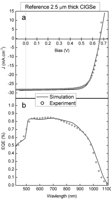
After the complete definition of the material and optical properties of the solar cell stack, we perform simulations of the Current-Voltage (J-V) curve and Spectral Response, and compare the results with the measurements performed on a reference 2500 nm CIGSe solar cell.
II.2.b) Modeling of current-voltage and spectral response
The CIGSe absorber thickness taken as the default thickness for a reference solar cell is 2500 nm. Figure 2.a shows a superposition of the J(V) curve of an experimental (dots) and a simulated (solid line) reference CIGSe solar cell and Figure 2.b shows the corresponding external quantum efficiencies.
Figure 2. Comparison between a state of the art 2500 nm CIGSe solar cell from Würth Solar
From the J-V curves presented figure 2.a, the photovoltaic parameters of the SCAPS baseline solar cell are:
Voc = 667 mV, FF = 73.9%, Jsc = 28.6 mA.cm-2 and Eff = 14.1%
Which are similar to those of the experimental reference CIGSe solar cell are: Voc = 663 mV, FF = 73.3%, Jsc = 28.1 mA.cm-2 and Eff = 13.7%
We can achieve a very good agreement between the simulated and the experimental results; we can also note that the slight differences are much lower than the usual spreading of the parameters observed on standard solar cells.
In addition, the Spectral Response curves presented in figure 2.b show a very close match between the experimental and the simulated curves. The CdS absorption in the UV range is well reproduced, along with the CIGSe absorption plateau in the visible range. The curves however slightly differ in the 800 nm to 900 nm, maybe due to some small interference effects that may appear in the ZnO layer for the experimental solar cell, even if the interfaces of a standard CIGSe solar cells is relatively rough. Also, the bandgap between the two curves seem slightly different. This is attributed to the fact that the ellipsometry data that are used to input the absorption coefficient has to be extrapolated in the vicinity of the bandgap due to the very low absorption of the material in the region, and therefore may lead to a lack of precision.
The agreement between experiments and simulations being good both for the J(V) characteristic and the spectral response, this validates our set-of parameters as a baseline state-of-the-art solar cell for simulating the influence of the absorber thickness on the photovoltaic parameters of the device. However, it is important to highlight the fact that the array of parameters to input in SCAPS is very large; As pointed by M. Burgelman et al. 40, one cannot be sure that another set of parameters does not exist and may lead to calculations which could be judged equally well as the one in figure 2. To prevent this from happening, we performed as many possible characterization on our material and compared it to state-of-the-art literature.
In the following, the thickness of the absorber will be progressively reduced and we will investigate on the evolution of the photovoltaic parameters together with proposing some interpretations.
II.3) Influence of CIGSe thickness on photovoltaic
parameters
In this section, we study the effect of the progressive reduction of the absorber thickness from the reference 2500 nm down to 100 nm on the J-V characteristics, the recombination currents in the device and the External Spectral Response (EQE). The doping level of the CIGSe, the mobility µ and the density of states in the conduction band and the valence band are considered homogenous throughout the layer. Using SCAPS 2.904, the absorber thickness is reduced from 2500 nm down to 100 nm starting from the baseline reference solar cell previously established in part I.
II.3.a) Modeling of the current-voltage curves
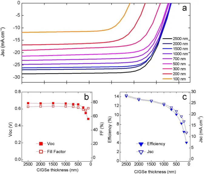
The figure 3 shows the simulated J-V curves (3.a) and the corresponding photovoltaic parameters (3.b and 3.c) for the different absorber thicknesses. We clearly see that two different regimes in the variation of the parameters emerge. The first one is from 2500 nm to around 500 nm, where the variations of the parameters is moderate. In this configuration, the absorber thickness is roughly higher or of the same order than the mean absorption length of the photons. The absorber layer can still be considered as relatively optically thick. In the second regime, from 500 nm to 100 nm, the variation of the parameters is much more abrupt; in this case, the absorber thickness and so the mean absorption length and the layer cannot be considered as optically thick anymore.
Figure 3. Simulated J-V characteristic (a) of CIGSe solar cells with different absorber
thicknesses from 2500 nm down to 100 nm (from dark blue to orange); (b) and (c) are the photovoltaic parameters of the solar cells extracted from the J-V curves.
In the first regime, both the open circuit voltage and the fill factor remain stable down to 500 nm absorber thickness with respective values close to 650 mV and 72-73 % respectively (figure 3.b). On the other hand, the short circuit current is linearly reduced from 28 mA.cm-2 for a 2500 nm thick absorber down to 20 m.A.cm-2 for a 500 nm absorber (figure 3.c). This drop is both related to non absorption of the photons due to the reduced absorber thickness and to an increased recombination current at the back contact (Jback). To illustrate
quantitatively the effect of an increase of the recombination current at the back contact when the efficiency decreases, we plot on figure 4.a the calculated back recombination current (calculation by SCAPS). The recombination current Jback increases from 1.2 mA.cm-2 at zero
voltage for the reference 2.5 µm thick absorber up to 2.8 m.A.cm-2 for the 0.5 µm absorber solar cell, so an absolute loss of 1.6 mA.cm-2. The rest of the losses are therefore attributed to non absorption of the photons due to an insufficient absorber thickness. The observed loss is however moderate, with a 29% relative decrease of the current for a removed thickness of about 80 % relatively to the initial 2500 nm absorber. Ultimately, the efficiency drops down to 11 % for a 500 nm thick absorber solar starting from a 14 % reference efficiency for a 2500 nm thick absorber; this efficiency loss is only related to the decrease of the Jsc as shown on
figure 3.c when reducing the absorber down to 500 nm.
Since the majority carrier concentration in the CIGSe is fixed at 2.1016 cm-3, it is possible to evaluate the space charge region width SCRW when no voltage is applied to the diode with
the simplified formula BI
a r
V qN
SCRW = 2
ε
ε
0 where VBI is the built-in potential (VBI~1 V), Nathe acceptor density, εr the relative permittivity of the CIGSe (εr = 13.6), and ε0 the absolute
vacuum permittivity (ε0 = 8.85.10-12 F.m-1). In our case, we obtain SCRW = 275 nm;
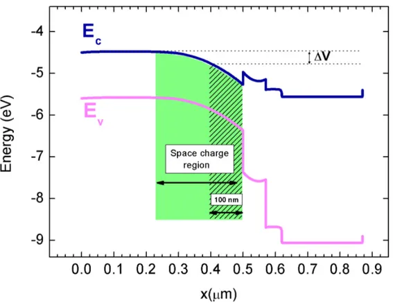
therefore, when the second regime is reached and the absorber thickness is lower than 500 nm (ultrathin absorber), it becomes of the magnitude (or even smaller) than the space charge region width and is fully depleted. This results in a ∆V shift of the conduction band that limits the Voc (460 mV for a 100 nm absorber solar cell) of the cell as it is illustrated figure 5. In this
case, the quasi fermi level separation is incomplete because of the early “cut” of the band bending region. This particular effect becomes noticeable for an absorber thickness at about 300 nm, thus very close to the value of the space charge region width. The Fill Factor is also slightly affected, although only for the 300 nm and 200 nm samples, where it decreases from its previously stable value of 72% down to 68%, before returning to its ~72% value for the 100 nm sample. The Jsc is dramatically decreased for the ultrathin absorbers (300 nm, 200 nm
Figure 4. (a) Back recombination current calculated for CIGSe solar cells with different
absorber thicknesses, from reference 2500 nm (dark blue curve) to 100 nm absorber (orange curve); (b) calculated band diagram of a 200 nm CIGSe solar cell under 4 different bias: 0 V, 0.3 V, 0.4 V and 0.6 V (from dark blue to light blue).
Figure 5. Band diagram of a thinned (500 nm) CIGSe solar cell, illustrating the effect on Voc
that has an ultrathinning of the absorber.
It might seem surprising that the back contact recombination is greatly reduced in our simulations for the samples 300 nm, 200 nm and 100 nm, as shown Figure 4.a; there is however a very consistent explanation to this. The absorber being completely depleted, every generated carrier is being driven to the p-n junction by the band bending and the strong electric field in the absorber prevents the generated carriers to drift to the back contact. Gloeckler & Sites 30 already highlighted this phenomenon when the absorber thickness is lower than the space charge region width and they showed that the Jsc is nearly independent of
the back contact and is only governed by the absorption of the CIGSe layer. The back recombination current curves figure 4.a for fully depleted absorbers are however not parallel to the rest of the curves (absorbers thicker than 500 nm) and they increase with a much more important slope: close to the operating point (450-500 mV), the back recombination currents of the ultrathin solar cells with fully depleted absorbers (300 nm, 200 nm and 100 nm) increase and exceed the recombination currents of the thicker absorber solar cells (> 500 nm). This is due to the fact that the positive polarization of the diode tends to reduce the band bending in the absorber by leveling the -p and the -n sides as it is schematized Figure 4.b.
Therefore, an increasing proportion of photons are absorbed in a quasi flat band region for ultrathin solar cell when applying a positive bias to the diode. While the 100 nm sample is still fully depleted at its much lower operating point, this is not the case for the 200 nm and 300 nm sample where a flat band region appears in the absorber. Therefore, back contact recombination is possible and it slightly reduces the photocurrent at this voltage; it directly affects the FF, which drops from 72% to 68% for the 200 nm and 300 nm sample as shown figure 3.b. For the 100 nm sample, the photocurrent is almost unchanged between V = 0V and the operating point, and so the FF recovers its initial level. As a result from the combined decrease of the Voc and the accelerated decrease of the Jsc, the efficiency is strongly reduced
from 11% for a 500 nm CIGSe solar cell down less than 4% for a 100 nm.
Eventually, the decrease of the short circuit current is clearly the dominant parameter limiting the efficiency of thinned solar cell although the open circuit voltage becomes an issue at ultrathin scale. In the perspective of using optical management techniques to improve the properties of the solar cell, it is important to investigate the spectral region where the losses occur and so spectral response of the solar cell.
II.3.b) Modeling of Spectral Responses
In this part, we simulate the External Spectral Response (External Quantum Efficiency EQE) of the solar cells when varying the absorber thickness. For these simulations, we used SCAPS 2.904 with exactly the same parameters as used previously for the J-V simulations. No interference effects within the device are being taken into account in these simulations. The obtained EQE curves are presented on figure 6. In the short wavelength region (λ = 400-600 nm), the absorption and carrier collection is almost not affected down to 500 nm of absorber thickness (first regime), with the EQE slightly decreasing from 83% for the reference 2500 nm thick CIGSe to 80% for the 500 nm thick CIGSe solar cell at λ = 550 nm. For the lower thicknesses however (second regime/ultrathin), an accelerated decrease of the EQE is observed. Despite the high energy of the incident photons, the film thickness is insufficient for a complete absorption on the whole spectrum. When the wavelength is increased, the losses due to the absorber thickness reduction become more important. From thicknesses between 2500 nm to 2000 nm, almost no change is observed; however, as the thickness is reduced down to 500 nm, the EQE is significantly reduced especially in the low energy range.
According to reference 30, this is partly due to an increased back contact recombination for carriers generated outside the depletion region close to the back contact, the non-absorption of the thinned CIGSe absorber being the other limiting factor. To support this assumption, we plot on figure 7 the photon absorption depth
α
δp = 1 in the CIGSe versus the wavelength, and the CIGSe thickness is schematically shown on the right side of the graph; this figure clearly illustrates the fact that a non negligible part of the spectrum is not absorbed when the CIGSe thickness is reduced from 2500 nm to 500 nm. In this range, the average absorption depth decreases by 100 nm on the spectrum (from about 1000 nm down to 900 nm). This is in direct relation with the decrease observed in this wavelength range in the EQE curves. Moreover, it confirms the fact that a non negligible part of the photons are also absorbed very close to the back contact, which tends to enhance the back contact recombination. For absorber thicknesses lower than 500 nm, the non absorption by the CIGSe becomes nearly the only parameter limiting the EQE as the back contact recombination is strongly reduced as previously stated. We see on figure 6 that for the 100 nm thick absorber, the EQE is dramatically lowered and it becomes less than 30% after 750 nm. Figure 7 shows that the absorber thickness is significantly lower than the absorption depth and so that the intercept between those two is at 510 nm (dark grey square); after this wavelength, the absorption of the 100 nm film is very poor as confirmed by the EQE simulation figure 6.
Figure 6. External Quantum Efficiencies of CIGSe solar cells with different absorber
thicknesses from 2500 nm down to 100 nm (from dark blue to orange).
Figure 7. Penetration depth in the CIGSe plotted with the photons incident wavelength. The
colored rectangles and the right side of the figure are illustration of the potential absorption of CIGSe layers with different thicknesses.
II.3.c) Conclusion
We have evaluated with numerical simulations the influence of reducing the absorber thickness in a CIGSe solar cell. It was possible to establish a “baseline” state of the art solar cell with SCAPS by using realistic parameters most of the time deduced from experimental data or from literature for the different layers composing the device. The baseline solar cell is in very good agreement with our state of the art experimental solar cell. In our simulations, the absorber thickness was varied from 2500 nm down to 100 nm while keeping constant the other parameters of the device. These simulations, although one-dimensional, gave us a fairly clear idea of the influence of the absorber thickness on the photovoltaic parameters of the solar cell. Two different regimes were identified:
- From 2500 nm down to 500 nm absorber thickness, the short circuit current is the only parameter that is affected by the absorber thickness reduction, decreasing from 28 mA.cm-2 (2500 nm CIGSe) down to 20 m.A.cm-2 (500 nm CIGSe). We attribute this drop to a combination of non absorption of low energy photons and back contact recombination affecting the carriers that are generated close to the back contact. Accordingly to the evolution of the Jsc, the efficiency decreases from 14% (2500 nm
CIGSe) down to 11% (500 nm). Although substantial, this variation is rather moderate when one considers the amount of active material that is removed, and at this stage, the CIGSe absorber could still be roughly considered as optically thick.
- From 500 nm down to 100 nm absorber thickness, the absorber becomes fully depleted, being thinner than the space charge region. The intense electric field forces the generated electrons to migrate to the p-n junction and almost completely prevents back contact recombination when no voltage is applied; accordingly to previous results from Gloeckler & Sites 30, the short circuit current is in this case only dependent on the absorption of the CIGSe. The absorption of ultrathin CIGSe layer is very low, which results in very important decrease of the photocurrent down to 12 mA.cm-2 for the 100 nm absorber solar cell; moreover, the fact that the absorber is thinner than the space charge region leads to an incomplete separation of the quasi fermi levels which limits the Voc (~460 mV for a 100 nm absorber solar cell). The
combination of these different losses dramatically reduces the efficiency of the solar which decreases down to 4% for a 100 nm CIGSe solar cell.
We have highlighted the main issues encountered when one reduces the thickness of the CIGSe absorber down to 100 nm. Both optical (light absorption) and electrical (limited voltage and back recombination) aspect are impacted in the perspective of very thin (500 nm) and ultrathin (100 nm) absorber solar cell. In the following part, optical simulations are done to suggest potential solutions that may allow to overcome the parameter’s limitations previously reported. Our solutions will first focus on the intermediate 500 nm CIGSe thickness (first regime), which already provides a substantial saving of material where the photocurrent is the only parameter that needs to be improved compared to a state of the art thick solar cell. Solutions to increase the efficiency of an ultrathin 100 nm CIGSe solar cell will also be presented.
II.4) Analysis of potential improvements for ultrathin
CIGSe solar cells
II.4.a) Introduction
In order to improve the performances of thinned absorber solar cells, an engineering of both the front and the back side of the device is needed. In this part, our study will focus on an intermediate 500 nm CIGSe, which cannot be considered as ultrathin, but offers interesting experimental short and mid-term perspectives along with a need for optimizations that can be realized as a first step in efficient thinner CIGSe solar cells. The purpose here is to improve the carrier collection and to increase the broadband light absorption in the active layer (CIGSe), which will allow the Jsc of the thinned CIGSe solar cell to match the Jsc of a standard
thick absorber device. The effect of reducing the losses in the supporting layers (front and back side) is modeled, by using an anti-reflection coating (ARC), a buffer layer with a wider bandgap, and a more reflective back contact. In addition, the effect of a p+ doped electron blocking back layer to reduce the back contact recombination is also presented.
II.4.b) Front and back side optical engineering for efficient light
management
Identifying the regions of the thinned absorber solar cell where the optical losses occur is a key issue for designing light management solutions. In the following, a complete CIGSe solar cell stack Mo-500 nm/CIGSe-500 nm/CdS-50 nm/ZnO:i-70 nm/ZnO:Al-400 nm is modeled and the light absorption of each layer depending on the wavelength is calculated. These calculations were performed at the Institut d’Optique by Dr. Nir Dahan and Prof. Jean-Jacques Greffet. For the optical modeling, the structure is considered as a stratified media with flat interfaces where the electromagnetic waves can be calculated at each position for any wavelength λ, incident angle θi, and polarization p. Here, the transfer-matrix method is
used to calculate the spectral absorption in layer m with thickness L by
Aλ(θi, m, p)=
S(m,0)−S(m,L)