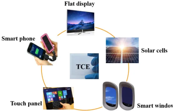
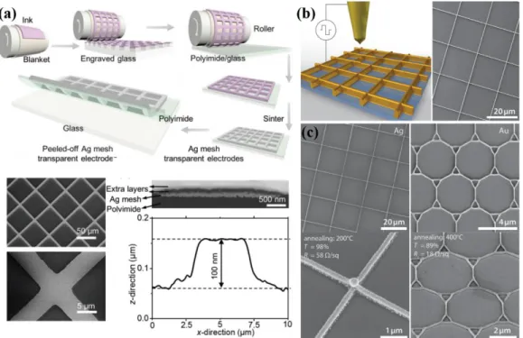
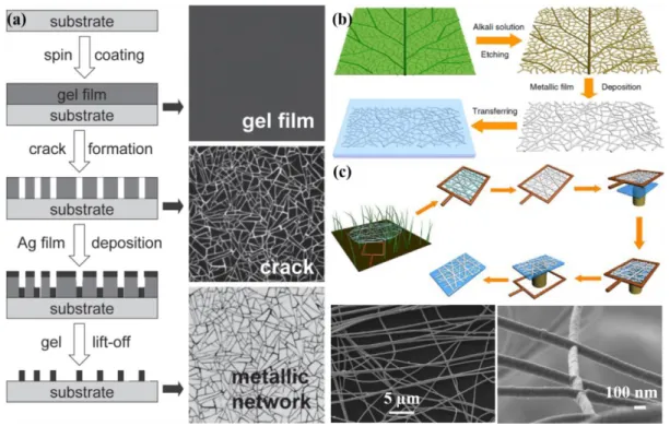
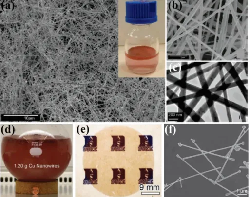
Metal nanowire-based transparent electrodes for smart window applications.
Texte intégral
Figure
Documents relatifs
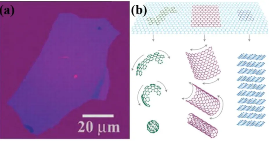
Integration of few kayer graphene nanomaterials in organic solar cells as (transparent) conductor electrodes.. Azhar Ali
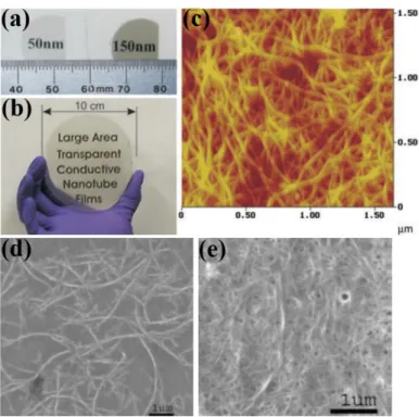
These measurements are performed using an atomic force microscope mode functioning contactThe obtained results on the preparation and characterization of transparent electrodes based
The obtained results on the preparation and characterization of transparent electrodes based on indium oxide ITO, shows that the ITO thin film has good transparency
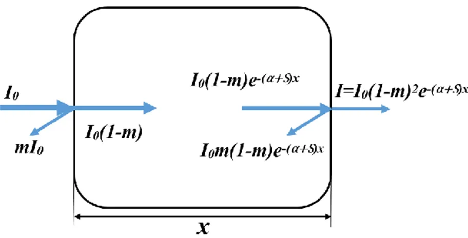
In the case of transparent conducting films with applications in photovoltaic devices, the measurements of the electrical resistivity during many successive heating and
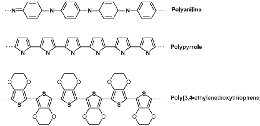
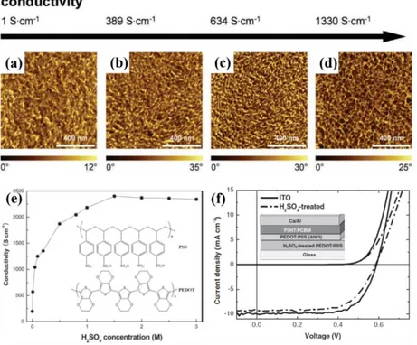
PEDOT:PSS (poly(3,4- ethylenedioxythiophene) polystyrene sulfonate) is the transparent conductive polymer the most often used as ITO free electrode, it is known to be a
Le chapitre 10 présente la qualité des rejets pluviaux stricts du site, l’efficacité de traitement de la mare et du filtre planté de roseaux, l’impact des
- incorporation de la solution (colorant/butanone) durant la synthèse du vernis sol-gel afin d’obtenir une incorporation optimale dans la matrice. Ces
Un cultivar de maïs, un de sorgho et un de melon ont été identifiés dans les plaines de sorgho repiqué du Chari Baguirmi (Tchad) ; trois cultivars de niébé, deux cultivars de
