UNIVERSITÉ DE MONTRÉAL
ELECTROSPINNING OF CONDUCTING POLYMER FIBERS FOR STRETCHABLE ELECTRONICS
FANNY BOUBÉE DE GRAMONT INSTITUT DE GÉNIE BIOMÉDICAL ÉCOLE POLYTECHNIQUE DE MONTRÉAL
MÉMOIRE PRÉSENTÉ EN VUE DE L’OBTENTION DU DIPLÔME DE MAÎTRISE ÈS SCIENCES APPLIQUÉES
(GÉNIE BIOMÉDICAL) MARS 2017
UNIVERSITÉ DE MONTRÉAL
ÉCOLE POLYTECHNIQUE DE MONTRÉAL
Ce mémoire intitulé :
ELECTROSPINNING OF CONDUCTING POLYMER FIBERS FOR STRETCHABLE ELECTRONICS
présenté par : BOUBÉE DE GRAMONT Fanny
en vue de l’obtention du diplôme de : Maîtrise ès sciences appliquées a été dûment accepté par le jury d’examen constitué de :
M. AJJI Abdellah, Ph. D., président
M. CICOIRA Fabio, Ph. D., membre et directeur de recherche
M. DE CRESCENZO Gregory, Ph. D., membre et codirecteur de recherche M. PELLERIN Christian, Ph. D., membre
DEDICATION
iv
ACKNOWLEDGEMENTS
I would like to start by thanking my supervisor and my co-supervisor, Professors Fabio Cicoira and Gregory de Crescenzo, for their help, advice and for giving me the opportunity to attend many interesting training sessions throughout the whole course of this project. I would also like to thank Marie-Hélène Bernier for giving me the opportunity to train students, as a lab assistant for the Microfabrication class.
I would like to thank the Professor Peter Grütter from McGill university and his group, and more particularly Maddy, for the help and advice they provided in the course of a collaborative project related to the one presented in these pages.
I am grateful to all the funding agencies and governmental groups without which this project would not have been possible: the Groupe de Recherche en Sciences et Technologies Biomédicales (GRSTB) and CMC Microsystems.I am also thankful to École Centrale-Supélec for giving me the opportunity to come to École Polytechnique Montréal for my studies. This experience abroad certainly was an instructive and enjoyable one.
I would like to thank Christophe Clément for his help and training on microfabrication, Daniel Pilon for his technical help on electrospinning and good advice, and Marie Richard-Lacroix for spending some of her time just before her thesis defense to discuss electrospinning with me. Your help and support were always valued.
I am also deeply grateful to all my colleagues and friends who helped me through this project, and more specifically to Zhihui and Eduardo for training me on general lab related work, Prajwal for training me on electrospinning, Shiming for his awesome knowledge about stretchable electronics and for his contagious motivation, and Gaia and Irina for their help and their totally not chocolate-free moral support. I’m thankful to all my other colleagues and former colleagues, Guido, Tania, Xu, Alexander, William, Francis, Jonathan, Côme, Yang, Xiang, Tian, Martin, Dominic, Zhaojing, Manuel, Michael, for all the time we spent together, both in lab and outside. To Bogdan, Shalin and Tom, that I had the pleasure to train in lab, I was happy that you all patiently listened to my explanations and asked way too many questions. Also, I would like to thank my other friends here, and especially Julien and Adrien for being like a family for the time they spent here, and Edwige, Sylvain, Alona, the Jacks (including the mad one) for always being a blast at parties, but also Alfredo, Olivier, Benji, and all the others for all the nice and crazy moments we spent together,
playing board games or spending the night cooking and talking. I was very fortunate to have you all around. I also was very lucky to have Alice, Anaïs, Gwen, Alex’, Baudouin, Charlie and Thibaut who all supported me even though we had an ocean and 6 hours of time difference between us. Thank you for giving me the motivation to come back home as soon as possible.
Finally, these last few lines are for my family. To my parents, who somehow managed to decide that it was ok to encourage me to fly across the Atlantic just so I could do what I wanted, to Peyot and Nanon, who went back to using Skype while pretending this did not bother them, and to Oscar and Candice, who always reminded me that half a world still was not quite enough to stop siblings from jokingly bickering: thank you, and I love you.
vi
RÉSUMÉ
L’électronique étirable est un domaine prometteur en ce qui concerne les applications au biomédical. En effet, les dispositifs étirables peuvent être utilisés pour remplir diverses fonctions, qui incluent l’électronique portable (ou les vêtements intelligents), la peau artificielle, et de façon plus générale l’ensemble des fonctions qui exigent d’avoir de l’électronique placée directement sur la peau apte à se conformer au style de vie du patient, par exemple pour de la surveillance quotidienne des constantes biologiques d’un patient. De nombreuses stratégies ont été mises en place jusqu’à présent pour produire de l’électronique étirable, cependant celles-ci peuvent être grossièrement séparées en deux catégories principales. Dans la première se retrouvent toutes les stratégies où les matériaux sont étirés grâce à l’utilisation d’une géométrie spécifique, tandis que la seconde catégorie comprend l’ensemble des matériaux qui sont intrinsèquement étirables. Ainsi, des formes spécifiques comme des fibres peuvent être utilisées pour améliorer la capacité à s’étirer d’un matériau autrement peu étirable, ce qui inclut des matériaux conducteurs comme les métaux ou certains polymères conducteurs et semi-conducteurs utilisés en électronique organique. Cependant, la mise en pratique de ces fibres requière l’utilisation d’une technique apte à aisément générer des fibres conductrices. Pour les applications en biomédical, les matériaux électroniques organiques présentent l’avantage sur l’électronique classique de posséder une bonne compatibilité avec les systèmes biologiques du fait de leur capacité à aisément faire l’interface avec le milieu biologique. Ils présentent aussi l’avantage pour ces applications de disposer d’une capacité à conduire à la fois les ions et les électrons.
Le but de ce projet de recherche est de démontrer la faisabilité de la fabrication de tels films, faits de nanofibres en polymère conducteur, qui maintiennent leur capacité à conduire le courant même lorsque ceux-ci sont étirés.
Bien que de nombreuses méthodes existent pour produire de telles fibres, l’électrofilage apparaît comme étant l’une des méthodes les plus simples pour réaliser des couches poreuses et non tissées de nanofibres, couches qui peuvent aisément se conformer à la surface de leur substrat. En combinant l’électrofilage avec une technique appelée la polymérisation en phase vapeur, nous avons fabriqué des nanofibres conductrices de poly(3,4-éthylènedioxythiophène) dopé avec de l’acide paratoluènesulfonique (tosylate, PEDOT:Tos) directement sur du polydiméthylsiloxane (PDMS), un élastomère organique siliconé. Cette méthode simple à deux étapes nous a permis de
produire des nanofibres de poly(3,4-éthylènedioxythiophène) dopé avec du tosylate (PEDOT:Tos) sur du PDMS. Des couches fibreuses non tissées composées de nanofibres conductrices possédant un diamètre moyen d’un peu moins de 700 nm ont ainsi été obtenues directement sur le PDMS. Nous avons caractérisé ces fibres pour étudier leur comportement électrique lorsqu’une tension était appliquée à leurs extrémités. Ces tapis de fibres ont alors pu être étirés tandis qu’un voltage fixé appliqué directement dessus forçait l’écoulement d’un courant à l’intérieur des films, courant qui a été mesuré. Cela nous a permis de démontrer que ces films possédaient la capacité de s’étirer jusqu’à 140% de leur longueur initiale sans variation majeure de la quantité de courant s’écoulant dans les films.
viii
ABSTRACT
Stretchable electronics is a promising field for biomedical applications. Stretchable devices can be used for various purposes, including wearable electronics (or smart clothes), artificial skin, and more generally for any purpose requiring to have on-skin electronics that conform to the lifestyle of the patient, for example day-by-day biomonitoring. Many strategies have been used so far to produce stretchable electronics, however these can be split between two main categories. In the first one are the materials that stretch due to a specific geometry, while in the second category are the materials that are intrinsically stretchable. Specific shapes such as fibers can thus be used to improve the stretchability of an otherwise poorly-stretchable material, including conductive materials such as metals or conducting and semi-conducting polymers used in organic electronics. However, the practical application of fibers in stretchable electronics requires the use of a technique that can easily yield conductive fibers. For biological applications, organic electronic materials present the advantage over conventional electronic materials to possess a good compatibility with biological systems due to their ability to easily interface with the biological milieu and their mixed ionic / electronic conduction.
The objective of this research project is to demonstrate the fabrication of such films, made with conductive polymer nanofibers that can still conduct the current even when stretched.
Although many methods exist to produce such fibers, electrospinning is one of the easiest ways to directly make non-woven porous nanofiber mats that can conform to the surface of their substrate. By combining electrospinning with vapor phase polymerization, we fabricated conductive nanofibers of poly-(3,4-ethylenedioxythiophene) doped with paratolenesulfonate (tosylate, PEDOT:Tos) directly on polydimethylsiloxane (PDMS), an organosilicon elastomer. Non-woven fiber mats composed of conductive nanofibers with an average diameter of around 700 nm were obtained directly on PDMS. We characterized these fibers to study their electrical behavior when a strain was applied to them. These mats were then stretched while the current flowing inside them was measured, at fixed voltage. This allowed us to demonstrate a stretchability up to 140% of the initial length without major variation of the current flowing in the mats.
TABLE OF CONTENTS
DEDICATION ... III ACKNOWLEDGEMENTS ... IV RÉSUMÉ ... VI ABSTRACT ... VIII TABLE OF CONTENTS ... IX LIST OF TABLES ...XII LIST OF FIGURES ... XIII LIST OF SYMBOLS AND ABBREVIATIONS... XIXCHAPTER 1 INTRODUCTION ... 1
1.1 General context ... 1
1.1.1 Stretchable electronics ... 1
1.1.2 Organic electronics ... 2
1.1.3 Principles of electrospinning ... 2
1.1.4 Principles of vapor phase polymerization ... 3
1.2 Problematics ... 3
1.3 Research objectives ... 3
1.4 Organization of the memoir ... 3
CHAPTER 2 CRITICAL REVIEW OF LITERATURE ... 5
2.1 Stretchable electronics ... 5
2.1.1 Stretching non-stretchable materials ... 5
2.1.2 Organic materials for stretchable purposes ... 10
2.2 Fibers ... 12
x
2.2.2 Fabrication methods ... 13
2.2.3 Electrospinning ... 17
2.3 Vapor phase polymerization ... 38
2.3.1 Working principle of vapor phase polymerization ... 39
2.3.2 Production of PEDOT fibers using vapor phase polymerization ... 41
CHAPTER 3 MATERIALS AND METHODS ... 43
3.1 Substrate preparation ... 43
3.2 Electrospinning ... 44
3.2.1 Preparation of the mixture ... 44
3.2.2 Cleaning of the syringe ... 44
3.2.3 Electrospinning parameters ... 44
3.3 Vapor phase polymerization ... 45
3.4 Sample rinsing ... 46
3.5 Characterization ... 47
3.5.1 Diameter of the fibers ... 47
3.5.2 Electrical characterization during stretching ... 47
CHAPTER 4 ARTICLE 1: HIGHLY STRETCHABLE ELECTROSPUN CONDUCTING POLYMER NANOFIBERS ... 49 4.1 Article presentation ... 49 4.2 Authors ... 49 4.3 Abstract ... 50 4.4 Article ... 50 4.5 Acknowledgements ... 59 4.6 References ... 60
5.1 Patterning of the fibers ... 62
5.2 Complementary electrical measurements ... 63
5.2.1 Unrinsed fibers ... 63
5.2.2 PEDOT:Tos fibers with a strain-sensing behavior ... 64
5.3 Cell cultures ... 65
CHAPTER 6 GENERAL DISCUSSION ... 66
6.1 Main results ... 66
6.1.1 Appearance of the fiber mats before/after stretching ... 66
6.1.2 Current measurement while stretching ... 67
6.2 Future challenges ... 68
6.2.1 Preparation of the solution ... 68
6.2.2 Relative humidity during electrospinning ... 69
6.2.3 Limitations of using PDMS as the support for the fibers ... 69
6.2.4 Improving the stretchability ... 70
6.2.5 Testing the removal of the PVP core ... 71
CHAPTER 7 CONCLUSION AND RECOMMENDATIONS ... 72
BIBLIOGRAPHY ... 75
xii
LIST OF TABLES
Table 2.1: Effect of different parameters on the diameter and the morphology of electrospun fibers. ... 26
LIST OF FIGURES
Figure 2.1: Three-dimensional profile of a Au surface wave after release from 15% pre-stretch [34-35]. © 2004 IEEE ... 7 Figure 2.2: SEM image of an array of stretchable, 3-stage CMOS ring oscillators in a twisted
configuration. [36] © 2008 National Academy of Sciences ... 7 Figure 2.3: Finite element analysis (FEA) was used to estimate the internal stresses in several
copper track patterns in the idealized case considering linear behavior (Young modulus E = 117 GPa) of the materials and neglecting the influence of any substrate material. By taking a horseshoe shape instead of an elliptical shape with the same wavelength/amplitude ratio, the maximum internal stress was reduced from 3610 to 1942 MPa. Splitting up the track into four parallel narrow tracks leads to a further reduction from 1942 to 230 MPa. (a) Elliptic. (b) Horseshoe. (c) Multitrack horseshoe. [39] © 2007 IEEE ... 8 Figure 2.4: Optical image of a folded circuit (left) consisting of an array of CMOS inverters and
scanning electron microscopy image (center). The images on the right provide views at the folded edge (right top) and side (right bottom). [40] © 2009 John Wiley and Sons ... 9 Figure 2.5: Scheme of a compliant zinc carbon dry gel cell. The cell is based on pastes as electrodes,
chemically active cells, and an electrolyte gel to close the circuit. Intermixing and short-circuiting of the electrochemical power supply are prohibited by laterally separating the electrodes with an elastomer separator [50]. © 2010 John Wiley and Sons ... 10 Figure 2.6: Schematic illustration of nanofibers fabrication by direct drawing process from molten
poly(trimethylene terephthalate) (PTT). I, An iron or silica rod is approaching the molten PTT. II, The rod end is immersed into the molten PTT. III, The rod conglutinated PTT is being drawn out. IV, A PTT nanofiber is formed. [83] © 2008 Optical Society of America ... 14 Figure 2.7: Schematic diagram of a wet-spinning apparatus [88]. © 2007 Elsevier ... 15 Figure 2.8: Number of publications in the database Web of Science(TM) containing the words
"electrospinning", "electrospun" or "electrical spinning" since 1997. The histogram on the left shows the detail between 1997 and 2002, while the one on the right shows all the results for the years 1997 to 2016. The results were obtained on the 01/10/2017. ... 20
xiv
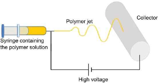
Figure 2.9: Schematic drawing of an electrospinning setup. The syringe is usually connected to a syringe pump to ensure a constant flow rate in the nozzle. The mandrel (or “collector”) can be made in different shapes and composed of different materials. It is usually grounded or put at a slightly negative voltage (around -3 kV), while the syringe is put at a high voltage (tens of kV). ... 21 Figure 2.10: First 1.4cm of a glycerin jet 4.66cm long, showing the structure known as Taylor cone
on the right, at the tip of the nozzle [137]. © 1969, The Royal Society ... 22 Figure 2.11: Evolution of the shape of a fluid drop. The time 0 was chosen as the time when the jet
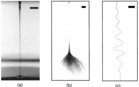
first appeared. The electrical potential was applied for a little more than 28 ms earlier. The first picture (-28 ms) thus shows the elongation of the drop into a cone-shape due to the electrical potential. The second (-8 ms) and third (-2 ms) pictures show the further elongation of the drop into a cone, followed by the apparition of the jet (0 ms). Finally, the shape rapidly changed into a rounder one, in the form of the Taylor cone (+32 ms). This last shape was stable as long as enough fluid was brought to the nozzle to compensate for the fluid lost in the jet [141]. © 2008 Elsevier ... 22 Figure 2.12: Jet images of a 2 wt% solution of PEO (MW = 2 000 000) in water during
electrospinning. (a) Stable jet (scalebar = 5mm); (b) unstable jet (scalebar = 5 mm, 1 ms exposure); (c) close-up of the onset of instability (scalebar = 1 mm, 18 ns exposure) [142]. © 2001 AIP Publishing LLC ... 23 Figure 2.13: Schematic diagram of an electrospinning jet, showing three different levels of bending
instability [141]. © 2008 Elsevier ... 24 Figure 2.14: A scanning electron microscopy (SEM) picture of beaded fibers [144]. © 1999
Elsevier ... 25 Figure 2.15: Scheme of various kinds of collecting systems used in electrospinning, showing (a) a
metal plate collector, (b) a rotating drum, (c) a triangular frame placed near a single plate and (d) a parallel dual plate. [151] © 2004 Elsevier ... 27 Figure 2.16: (A) Schematic illustration of the setup for electrospinning used to generate uniaxially
aligned nanofibers. The collector contained two pieces of conductive silicon stripes separated by a gap. (B) Calculated electric field strength vectors in the region between the needle and
the collector. The arrows denote the direction of the electrostatic field lines. (C) Electrostatic force analysis of a charged nanofiber spanning across the gap. The electrostatic force (F1) resulted from the electric field and the Coulomb interactions (F2) between the positive charges on the nanofiber and the negative image charges on the two grounded electrodes. Reprinted with permission from [161]. Copyright 2003 American Chemical Society. ... 28 Figure 2.17: Continuous as-spun nanofibers deposited on a rotating multi- frame structure [106].
© 2003 Elsevier ... 29 Figure 2.18: Schematic drawing of the electrospinning process with a rotating disk collector,
showing the jet path and the region where the bending instability rapidly grew into a conical envelope. This later changed into an inverted conical envelope with its apex on the rotating disk’s edge. The disk is made of aluminium and has an overall diameter of 200 mm and thickness of 5 mm [164]. DOI: https://doi.org/10.1088/0957-4484/12/3/329 © IOP Publishing. Reproduced with permission. All rights reserved. ... 30 Figure 2.19: On the left: scheme of a dual grounded ring configuration for the collection system.
On the right: once the fibers are formed, the ground on the right is rotated while the ground on the left stays stationary. This allows for the formation of a yarn. [151] © 2004 Elsevier 30 Figure 2.20: Aligning electrospun fibers with an auxiliary electric field [106]. © 2003 Elsevier. 31 Figure 2.21: A multiple-field technique to obtain aligned fibers [167]. © 2001 Elsevier ... 32 Figure 2.22: (a) Schematic illustration of fabrication of fibrous tubes by electrospinning technique
using 3D columnar collectors. 1: 3D columnar collectors. 2: relevant fibrous tubes. (w, working collector; pa, plane assistant collector; sa, stick assistant collector) (b) Fibrous tube with diameter of 500 μm (inset is the cross-section image). (c) SEM image of fiber assemblies of tube shown in panel b. Reprinted with permission from [169]. Copyright 2008 American Chemical Society. ... 33 Figure 2.23: Schematic of electrolyte-assisted electrospinning (ELES) to self-assemble electrospun
fibers. a) Experimental setup of ELES to self-assemble electrospun fibers on a collector made of an electrolyte solution (potassium chloride). b) Self-assembled nanofiber membranes on a curved surface. Scale bar: 10 µm [172]. © 2015 John Wiley and Sons ... 34
xvi
Figure 2.24: Schematic drawing of the setup used in [194] and chemical structures of MEH-PPV and P3HT (written here as PHT). © 2004 John Wiley and Sons ... 36 Figure 2.25: PEDOT:PSS/PEO fibers as “stranding fibers” trying to reach the spinning nozzle
[203]. © 2015 Elsevier ... 38 Figure 2.26: A typical procedure for deposition of conjugated polymer films by VPP. Alternative
methods, such as sublimation, have been used to achieve oxidant preapplication (Step I). [207] © 2012 John Wiley and Sons ... 39 Figure 2.27: Chemical reaction between EDOT and Tosylate leading to PEDOT:Tos [222-223]. ... 42 Figure 3.1: Glass slide (dark blue) with a home-made support (orange) attached on it. A PDMS
substrate (transparent lighter blue) is attached on top on the support. This configuration allows for an easier removal of the PDMS substrate after electrospinning by limiting the contact and thus the adherence between the PDMS and its support. The PDMS can also be removed by cutting if necessary. ... 43 Figure 3.2: Schematic drawing of the fibers structure before and after vapor phase polymerization
(VPP). The yellow coating also contains imidazole (not specified on the schematic), while the PVP core (in grey) also contains Fe3+, Tos and Imidazole. ... 46 Figure 3.3: Setup used to measure the current while stretching the samples. EGaIn is used as a
liquid metallic electrode to ease the connection between the fibers (in blue) on the PDMS substrate and the copper wires. ... 48 Figure 4.1: Process used to obtain fibers of PEDOT:Tos. A mixture containing PVP, Fe(III)Tos
and Imidazole is electrospun directly on a PDMS substrate attached to a rotating cylindrical collector. The applied voltage is 20 kV, and the distance is 15 cm (Step 1). The PDMS covered with fibers is placed inside a chamber at atmospheric pressure. A crucible containing EDOT is warmed at 50°C to evaporate the monomer, thus allowing the polymerization of PEDOT:Tos on the fibers (Step 2). The fibers are rinsed with ethanol to remove the unreacted chemicals (monomer and oxidant) and to dissolve the PVP core of the fibers. Removing the PVP core allows for better long-term stability of the fiber mat, by preventing the PVP from melting by absorbing ambient water later. ... 54
Figure 4.2: PEDOT:Tos fibers on PDMS obtained after 3 min of electrospinning at 20 kV and 15 cm nozzle-collector distance, 30 min of VPP and rinsing in ethanol. a) SEM micrograph of a network of fibers. The fibers appear to be fused together at the intersections, which suggests an easier conduction of the current at the junctions. A few fibers show beaded structures. The “flatness” of the fibers is due to the removal of the PVP core following rinsing with ethanol (the scale bar is 20 µm). b) Close-up of one PEDOT:Tos fiber (scale bar is 1 µm) with a diameter of about 600 nm. c and d) optical microscopy of a network of fibers c) before and d) after a 100% stretch. The white arrow shows the stretching direction, and the oval highlights a small tear in the network, as well as a few broken fibers (the scale bars in c) and d) are 20 µm). ... 55 Figure 4.3: a) Current vs time plots for PEDOT:Tos fibers on PDMS. A logarithmic scale is used
for the current. The sample was stretched in cycles, from 20% to 140% strain percentages at 0.1 cm/s. Five consecutive cycles of stretching and release were performed at each of the different strains percentage between 20% and 140%. The PDMS substrate broke at 160% strain. The samples were kept in each state (stretched or released) for a resting time of 1min. Inset: scheme of the setup used for this measurement. EGaIn was used for the connection between the fiber mat and the copper wires. The arrows show the stretching direction of the sample. b) Current vs time plots for a similar sample stretched at 100% strain percentage for 50 cycles, with a stretching speed of 0.1 cm/s. One stretching cycle consisted of stretching at 100% strain during 15 s followed by release to the initial length during 15 s. The 50 cycles were performed without pause. Inset: Close-up of the behavior of the current during three cycles, with indication of the time during which the strains were applied and released. The samples were 1.5 cm long and 1 cm wide. The fibers were obtained after 3 min of electrospinning at 20 kV and 15 cm nozzle-collector distance, 30 min of VPP, and rinsing with ethanol. The measurements were made at 200 mV. ... 57 Figure 5.1: Patterned PEDOT:Tos nanofibers on PDMS. These were produced using a parylene
mask. The patterns shown are 800 µm wide and 2 mm long. The top patterns appear to be slightly deformed, due to small wrinkles on the PDMS or on the parylene during the patterning. Bubbles under the PDMS are also visible on the top left and right corners, as well as in the bottom right and on the pattern. ... 62
xviii
Figure 5.2: Current vs time for fibers obtained after 3min of electrospinning and VPP on PDMS, without ethanol bath, with a voltage of 200mV applied. The initial 120% stretching leads to a drop in the current. After this first drop, the sample was brought back to its initial position, but no recovery of the current was observed. ... 63 Figure 5.3: Current vs time for fibers obtained after 3min of electrospinning and VPP on PDMS,
with a voltage of 200mV applied, when the PDMS underwent a UV-ozone treatment before the electrospinning, stretched at 50% 2 times, followed by a third stretch at 100%. The PDMS film broke during this third stretch. ... 64
LIST OF SYMBOLS AND ABBREVIATIONS
Ag silver
Al aluminium
Ar argon
Au gold
BEC block copolymer elastic conductors CHCl3 chloroform
CNT carbon nanotube
CTAB cetyl trimethylammonium bromide CVD Chemical Vapor Deposition DBSA dodecylbenzene sulfonic acid DEHS di(2-ethylhexyl) sebacate DMF N,N-Dimethylformamide DMSO dimethylsulfoxide
ECM extracellular matrix
EDOT 3,4-ethylenedioxythiophene EGaIn eutectic gallium indium
F8BT poly[(9,9-dioctylfluorenyl-2,7-diyl)-alt-co-(1,4-benzo-{2,1′,3}-thiadiazole)] Fe(III)Tos iron(III) p-toluenesulfonate, or ferric p-toluenesulfonate
FeCl3 iron(III) chloride, or ferric chloride FeCl3·6H2O ferric chloride hexahydrate
FTIR Fourier transform infrared spectroscopy
GO graphene oxide
xx
ICP Intrinsically Conducting Polymer LED light emitting diode
MEH-PPV poly[2-methoxy-5-(2-ethylhexyloxy)-1,4-phenylenevinylene]
Mw Molecular weight
N2 nitrogen
NaDEHS di(2-ethylhexyl) sulfosuccinate sodium salt
NW nanowire
oCVD oxidative chemical vapor deposition OECT organic electrochemical transistor P3DDT poly(3-dodecylthiophene)
P3HT poly(3-hexylthiophene) PAN polyacrylonitrile PANI polyaniline
PANI:HCSA polyaniline doped with aphorsulfonic acid PCBM (6,6)-phenyl-C61-butyric acid methyl ester PCL poly(ε-caprolactone)
PDMS polydimethylsiloxane
PEDOT poly-(3,4-ethylenedioxythiophene)
PEDOT-PIL poly-(3,4-ethylenedioxythiophene) mixed with poly(ionic liquid)
PEDOT:PSS poly-(3,4-ethylenedioxythiophene) doped with poly(styrenesulfonic acid) PEDOT:Tos poly-(3,4-ethylenedioxythiophene) doped with tosylate
PEEA poly(ether-b-ester) PEO poly(ethylene oxide)
PI polyimide
PIL poly(ionic liquid)
PLGA poly(lactide-co-glycolide) PMMA poly(methyl methacrylate) PPV poly(phenylene vinylene)
PPy polypyrrole
PPy-Tos polypyrrole with p-toluenesulfonate
PS polystyrene
PSS poly(styrenesulfonic acid) PTT poly(trimethylene terephthalate)
PU polyurethane
PVA poly(vinyl alcohol)
PVF2-TrFE poly(vinylidene fluoride-trifluoroethylene) PVP poly(vinylpyrrolidone)
SEBS poly(styrene-co-ethylenebutylene-co-styrene) SEM Scanning Electron Microscopy
SIBS poly (styrene-block-isobutylene-block-styrene) SWCNT single-walled carbon nanotubes
Tos tosylate, or p-toluenesulfonate
UV ultraviolet
VDP Vapor Deposition Polymerization VPP Vapor Phase Polymerization Zonyl fluorosurfactant Zonyl-FS300
1
CHAPTER 1
INTRODUCTION
1.1 General context
Healthcare in our societies is currently seeking for innovative solutions, mostly because of the aging of the population and the rise in medical costs. One of the main objectives is personalized healthcare [1-2], which would give patients access to a more personalized medicine. A primary role in the creation of personalized healthcare systems will be played by materials and technologies that could allow the creation of more affordable and more specific healthcare systems. Systems and devices for personalized healthcare need to be both inexpensive and easy to use for non-professionals, so that patients can safely and properly monitor their conditions from home whenever required. Moreover, a more personalized access to healthcare should limit the use of invasive devices while promoting systems that are as non-obtrusive as possible [3]. For instance, diagnostic devices, such as biosensors, need to become less bulky, more flexible and stretchable, so that they can be put in direct contact with the human skin or integrated in wearables [4]. This would allow them to even be used as ambulatory systems, thus leading to easier ways to monitor the patients over long periods of time [5].
1.1.1 Stretchable electronics
Wearable and on-skin electronics require devices that maintain their electrical properties when a tensile strength is applied. These are known as “stretchable electronic devices”. The human skin can be stretched to a about 30% without breaking [6], although some authors report variations from 35% to 115% in the human population [7]. These differences in the literature can be explained by the changes in elasticity underwent by the human skin during life, since babies’ skins are a lot more elastic than seniors’ skins. With these values in mind, it appears important to ensure that a device in direct contact with a patient’s skin would be able to stretch at least as much, without rupturing or undergoing important changes that would render it unable to function. Stretchability of electronic materials can be achieved using two different and complementary approaches, i.e. by shaping the electronic components in a specific geometry, or by exploiting the intrinsic mechanical properties of the materials used.
1.1.2 Organic electronics
Biomedical applications such as biosensing require stretchable devices possibly made of materials that can be either functionalized or fine-tuned during their synthesis or the processing and that can be interfaced with a biological milieu. These specifications are achieved with organic conductors and semiconductors.
Electrical conductivity in organic materials was discovered in the beginning of the 1970’s by H. Shirakawa, A.J. Heeger and A.G. MacDiarmid [8]. This discovery, that opened up the field of organic electronics, was awarded the Nobel Prize in 2000 [9]. Since then, organic electronic materials have been widely investigated due to their exciting properties for lighting, electronics and energy applications. There are a wide range of conducting or semi-conducting organic materials available, with virtually as many choices for one specific application. What is more, they are easily processed from solutions, and they allow ionic and electronic conduction, which allows them to be used as an interface with the biological milieu [10-11]. All these properties are intriguing for biological applications and thus lead to a wide investigation of these materials for biomedical applications.
1.1.3 Principles of electrospinning
During this work, a technique called electrospinning was used to obtain fibers of organic conducting polymers. This method consists of using an electric field between two metallic parts (one charged and one grounded) in order to cause a liquid to go from a nozzle (usually the charged part) to a mandrel (usually the grounded part) in the form of a jet, if the mixture presents satisfactory mechanical properties. The mixture can either contain a polymer in solution or a molten polymer. In the latter case, the technique is sometimes called “melt electrospinning”.
The jet formed between the nozzle and the mandrel solidifies. This is done either by evaporation of the solvent used or by solidification of the molten polymer (case of the melt electrospinning). This allows to collect fibers made of the mixture materials. Electrospinning will be discussed more in detail in Chapter 2.
3
1.1.4 Principles of vapor phase polymerization
Another important technique called Vapor Phase Polymerization (VPP) was used during this work. In VPP, a monomer is evaporated in a closed chamber in the presence of a film containing an oxidant (or polymerization initiator). The evaporated monomer reacts with the oxidant and polymerizes directly on the film. This technique, when combined with electrospinning, allows to obtain fibers of conducting polymers. This will be discussed more in Chapter 2.
1.2 Problematics
This memoir focuses on the following problematics:
- How to produce stretchable conducting polymer fibers able to follow the natural human movements of the skin?
- Is it possible to pattern such materials to obtain a functioning device usable for complex applications?
1.3 Research objectives
This work was based around several objectives:
- The production of conducting organic fibers, first on a flexible substrate then on a stretchable one;
- The characterization of the stretchable fibers;
- The patterning of the obtained fibers to fabricate a functioning device usable for complex applications.
1.4 Organization of the memoir
This introductory chapter presented the context, the problematics and the research objectives that this memoir is meant to tackle. This introduction is followed by six other chapters. Chapter 2 consists of a literature review about the main topics of this work, i.e. stretchable electronics, electrospinning and vapor phase polymerization. Chapter 3 explains the different materials and methods used during this memoir. This chapter is divided into several sections, explaining substrate preparation, formation of the fibers with a method using a combination of electrospinning and
vapor phase polymerization, and their characterization. Chapter 4 is comprised of the article related to this work as it was submitted, and thus also includes the main results of this project. Supplementary results are presented in Chapter 5. Chapter 6 consists of a discussion, leading to conclusion and perspectives in Chapter 7.
5
CHAPTER 2
CRITICAL REVIEW OF LITERATURE
2.1 Stretchable electronics
Stretchability is a crucial property for several non-invasive biomedical applications, including artificial muscles [12], artificial skin [13-14], and on-skin devices [15], a category of systems placed directly on the user’s skin in a conformable way, while being mechanically undetectable for the patient. Stretchable electronics can be used to achieve different functions, e.g. strain sensing, bio sensing, radio frequency induction, electrical sensing for the heart or the brain, motion detection [16]. By using stretchable electronic devices, a higher conformability to living tissues can be achieved [17], allowing for a better monitoring of biological parameters (e.g. cardiac rate, temperature, strain due to the contraction of the muscles, biomolecules concentrations) without putting any unnecessary strain on the patient’s daily life [18]. Examples are stretchable sweat biosensors [19], heart rate monitoring devices [20] or techniques like surface electromyography [21]. As mentioned in the introduction, two different strategies can be used to achieve this intriguing property. The first one is to use specific shapes with particular geometrical properties that allow to get usually non-stretchable materials to stretch, using the fact that any material in thin form will be able to bend [22]. This method is mostly used for traditional electronic materials, since most of them are non-stretchable and it will be discussed in more detail later in this section. The second strategy is to use intrinsically stretchable materials to achieve the stretchability of the whole device. These two strategies can also be combined, particularly in organic electronics. Below I will discuss the methods used to stretch both non-stretchable materials for conventional electronics (e.g. metals) and organic electronic materials.
2.1.1 Stretching non-stretchable materials
Several methods have been developed to achieve stretchability with materials that are intrinsically non-stretchable. Most of these methods are based on the conversion of stretching motions into microscopic bending strains, thus linking stretchability to a more easily achievable flexibility. The peak strain experienced by a film during bending is linked to the substrate thickness, the film thickness and the radius of curvature according to the following equation (Equation 2.1) [23]:
𝜀 = (𝑑𝑓+ 𝑑𝑠
2𝑟 ) × 100%
Equation 2.1: Relation between ε the peak strain, df the thickness of the film, ds the thickness of the substrate used, and r the curvature radius
The bending strain can be converted into tensile strain by using coiling and buckling [24], thus using flexibility to achieve stretchability. This means that by locally improving the flexibility of the materials with shape-engineering, stretchability of the whole structure can be achieved.
As for the methods used, they are diverse and require different levels of shape-engineering. Some groups focused on directly using the surface shape of the film deposited on top of a stretchable substrate, with the “buckling” method using vapor deposition or lamination directly on pre-strained elastomers used as substrates [25-26]. Once released, the film compresses and forms buckles, leading to the conversion of the stretching motions into unbuckling of the structure [27]. This leads to structures such as conductive “surface waves” that can be stretched flat [28] (Figure 2.1) and “wavy” silicon electronics [29-30]. These structures were even used in fully integrated circuits using single crystalline silicon in a wavy structure on stretchable elastomers [31]. In these different cases, the top structure is designed in such a way that it changes its form in order to accommodate the strain exerted on the whole device, while being mechanically supported by the underlying polydimethylsiloxane (PDMS) substrate, a clear semi-transparent silicon-based organic polymer widely used in stretchable devices. Once the force stops, the elastomer ensures that the original shape is restored. However, this is not the only available solution to obtain stretchable devices from non-stretchable materials. The controlled formation of micro-cracks during stretching on a film formed directly on a stretchable substrate can also ensure the uninterrupted stretchability and the conduction using percolated pathways [32]. Unfortunately, these quite simple methods yield materials with a limited ability to stretch: the films cannot be stretched more than a few tens of percent of their initial length without using a few tricks to boost the performance. Such “tricks” lead to a stretchability that can be improved up to 100%. This is done by increasing the roughness of the substrate, by pre-stretching it, and by raising the thickness of the metallic layer deposited [33].
7
Figure 2.1: Three-dimensional profile of a Au surface wave after release from 15% pre-stretch [34-35]. © 2004 IEEE
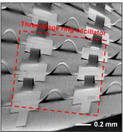
Figure 2.2: SEM image of an array of stretchable, 3-stage CMOS ring oscillators in a twisted configuration. [36] © 2008 National Academy of Sciences
Other groups rely on engineering the shape of the conducting materials in order to improve their stretchability. The shapes used to achieve this goal range from simple structures, such as highly stretchable (up to 370%) long metallic nanowires (NWs) [37] or hexagonal and triangular metallic nanosheets [38], to more complex structures, such as 3D pop-up structures that flatten when stretched [36] (Figure 2.2), or 2D ellipses and variations of horseshoe-like shapes [39] (Figure 2.3),
or 2D serpentine meshes [40] (Figure 2.4). These more complex shapes can yield stretchability to up to 300% [41].
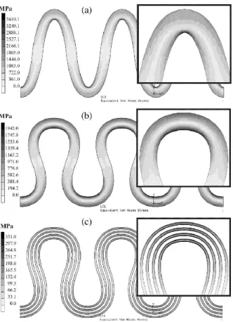
Figure 2.3: Finite element analysis (FEA) was used to estimate the internal stresses in several copper track patterns in the idealized case considering linear behavior (Young modulus E = 117 GPa) of the materials and neglecting the influence of any substrate material. By taking a horseshoe shape instead of an elliptical shape with the same wavelength/amplitude ratio, the maximum internal stress was reduced from 3610 to 1942 MPa. Splitting up the track into four parallel narrow tracks leads to a further reduction from 1942 to 230 MPa. (a) Elliptic. (b) Horseshoe. (c) Multitrack horseshoe. [39] © 2007 IEEE
9
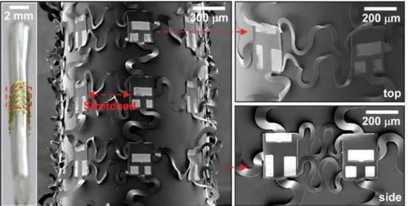
Figure 2.4: Optical image of a folded circuit (left) consisting of an array of CMOS inverters and scanning electron microscopy image (center). The images on the right provide views at the folded edge (right top) and side (right bottom). [40] © 2009 John Wiley and Sons
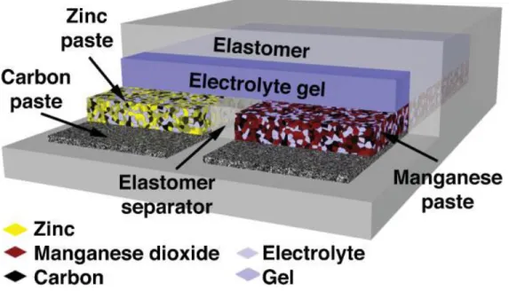
Silver (Ag) has been widely used to improve the conductivity of stretchable materials, either in the form of nanowires (NWs) or as flakes. Ag NWs embedded inside a PDMS elastomer were reported [42], while Ag NWs were also used with a carbon nanotubes (CNTs) percolation network to achieve conductive films that could be stretched to up to 460% before losing their conductive properties [43]. The use of CNTs or single-walled carbon nanotubes (SWCNT) was also widely studied and yields good results when trying to obtain stretchable electronics [44-46], allowing some groups to obtain conductivities as high as 100S/cm for films that could be stretched at more than 100% [47] while others managed to maintain a conductive behavior with strains superior to 700%, although they noticed the appearance of an increasing number of non-conductive areas the more they stretched their films [48]. Conductivities ranging from 5710 S/cm (at 0% stretch) to 20 S/cm (at 140% stretch) were also achieved by adding materials such as silver flakes in the CNTs structures [49]. The use of carbon paste supporting metallic pastes has also been reported for printable stretchable electronics. This method also required the use of an electrolyte gel to ensure the electrical contact between the two metals. The devices were completed by enclosing the pastes and the gel inside an elastomer structure (Figure 2.5), thus ensuring that the metallic pastes do not physically contact with each other during the stretching [50]. Graphene oxide (GO) was also used several times. In particular, it was used in combination with Ag NWs for a fully-stretchable LED
[51]. Carbon-based inks were also used to print fully stretchable devices embedded inside highly stretchable elastomers, by using a method called embedded 3D printing [52]. Finally, transfer methods allow for the production and patterning of the films on a solid substrate before transferring them on stretchable substrates such as PDMS [53]. All these solutions allow for the use of non-intrinsically stretchable organic and inorganic materials in complex systems.
Figure 2.5: Scheme of a compliant zinc carbon dry gel cell. The cell is based on pastes as electrodes, chemically active cells, and an electrolyte gel to close the circuit. Intermixing and short-circuiting of the electrochemical power supply are prohibited by laterally separating the electrodes with an elastomer separator [50]. © 2010 John Wiley and Sons
2.1.2 Organic materials for stretchable purposes
The strategy based on shape-engineering of the materials is not solely limited to purely inorganic materials. Some authors developed devices using non-stretchable platforms called “islands” connected by stretchable organic electronics; by using the geometry of the elastomer substrates, the strain can be limited to the connections, thus protecting the more brittle electronics [54]. Other authors used matrix shapes [55] or honeycomb meshes [56] to obtain fully stretchable organic devices.
11
Another strategy using both organic and inorganic is to include organic materials such as polyacrylate composites [57] in the conducting materials to obtain stretchable metallic-organic devices. The opposite strategy of adding inorganic materials, in particular conductive nanoparticles or CNTs, into organic elastomers can also yield good results, with a stretchability as high as 600% obtained by including silver flakes into a polyurethane (PU) elastomer [58].
However, due to the large spectrum of mechanical properties shown by organic materials, intrinsically stretchable organic materials are also widely studied for stretchable devices, to be used either alone or in combination with a shape designed to improve the stretchability of the system. Simple films made of poly-(3,4-ethylenedioxythiophene) doped with poly(styrenesulfonic acid) (PEDOT:PSS), a widely used conducting polymer, mixed with a fluorosurfactant, for example Zonyl-FS300 (Zonyl), and with dimethylsulfoxide (DMSO) as a secondary dopant already yield good stretchability results [59]. It was also reported that using the slightly brittle surface created on PDMS by the UV-ozone treatment allowed the formation of wavy structures in films composed of PEDOT:PSS mixed with Zonyl and DMSO. These structures allowed the films to be reversibly stretchable with conductivities as high as 550S/cm for a 0-188% stretchability [60]. PEDOT:PSS can also be used with other compounds, such as a blend of regioregular poly(3-hexylthiophene) (P3HT) and (6,6)-phenyl-C61-butyric acid methyl ester (PCBM) (P3HT:PCBM) and processed as a film on a PDMS substrate for applications in stretchable organic solar cells in a sandwich structure. This resulted in a 0-25% stretchability, with a surface resistivity of around 750 Ω/sq [61]. In another work, PEDOT mixed with a poly(ionic liquid) (PIL) or PEDOT-PIL was used to increase the miscibility of PEDOT with a non-conducting elastomeric polymer called poly(ether-b-ester) (PEEA) so that an homogeneous blend of the two polymers could be obtained. A stretchability as high as 350% was obtained, although the resultant surfacic resistivity was quite high, with a value of 8.108 Ω/sq [62]. More recently, a blend of PEDOT:PSS and PU was reported for a pressure sensor using PDMS shaped as a micro-pyramids array. The blend was used to form electrodes on top of the pyramids, and thus was required to keep a high conductivity (around 168 S/cm for a blend with 60 wt% PU, and around 120 S/cm for the 73 wt% PU blend) [63]. Work was also done to improve the geometry of the PEDOT:PSS used, for example by making nano-arches out of a nanowire of PEDOT:PSS that led to a stretchability as high as 240% without having to compromise on the electrical conduction, keeping a 200S/cm conductivity during the whole stretching [64].
Some of these organic materials achieve a conductivity high enough to be used as electrodes, as reflected in the use of stretchable polypyrrole (PPy) with p-toluenesulfonate (Tos), or PPy-Tos electrodes for battery applications. The PPy-Tos electrodes are placed on top of an Au/poly (styrene-block-isobutylene-block-styrene) (SIBS) substrate and can stretch up to 30%, with a surfacic resistivity going up from 171 Ω/cm2 (0% stretch) to 240 Ω/cm2 (30% stretch) after 2000 cycles [65]. High conductivity in stretchable electronics is also achieved with more complex structures, such as “block copolymer elastic conductors” (BEC) based on conductive polyaniline (PANI) and the block copolymer poly(styrene-co-ethylenebutylene-co-styrene) (SEBS) [66], or by using SWCNT-polymer composite electrodes [67]. Metallic conductivities were also achieved by directly injecting the liquid metal eutectic Gallium Indium (EGaIn) in hollow fibers made of SEBS. This resulted in a very high conductivity, coupled with an ultra-high stretchability of 700% [68].
2.2 Fibers
2.2.1 Interest of fibers
One-dimensional nanostructures such as nanofibers, nanotubes or nanowires have been largely studied in the recent years. This is due to their intriguing properties related to their small size. Fibers present a real interest in stretchable and wearable devices. They exhibit a good flexibility and tensile strength, and can thus be stretched, twisted, bent or sheared [69]. Due to their mechanical properties and their usually light weight [70], they can be used for textiles and thus are the more obvious candidates for wearable electronics or intelligent clothing [44] [71] and more specific applications such as artificial muscles [12]. They also exhibit a high surface area and a good flexibility regarding their surface functionalization [72]. These properties make them excellent candidates to achieve both the stretchability and the high functionality required for applications in the biomedical field, in particular for wearable biosensors. Conducting fibers thus present the double advantage of being usable for wearable applications and for electronic applications, rendering it possible for the development of smart textiles [73] for smart or intelligent clothing [74] that could then be functionalized for specific applications. Due to the fibers flexibility and stretchability, it would allow for intelligent wearable systems that are non-obtrusive, by avoiding bulky options for biomedical applications [5]. Sensors based on fibers have already been
13
demonstrated by several groups [75-76], rendering it possible to use them more widely for biomonitoring in the future. The path of wearable sensors has already been opened by several groups [77-80] but more work on the materials is necessary to improve the already encouraging results obtained.
2.2.2 Fabrication methods
Several methods exist to produce fibers from polymers. This section will focus on explaining some of the main methods used in literature by different groups. As for the electrospinning process, it will be discussed in the next section.
2.2.2.1 Drawing
Drawing is a method consisting of pulling a mixture over a relatively long distance to obtain a thin liquid fiber. Two drawing techniques are typically employed: dry spinning and melt spinning, which differ by the way the fibers are obtained from the original mixture. Once the mixture is drawn, the evaporation of the solvent (dry spinning) or the solidification of the whole mixture due to cooling (melt spinning) yields solid one-by-one fibers. In the case of melt spinning, heating of the mixture before drawing is necessary [81]. The melt spinning technique is explained in Figure 2.6. This method requires the use of a highly viscoelastic material that can undergo strong deformations and still stay cohesive enough to avoid ruptures during the drawing process due to stress [82]. If the material used satisfies this constraint, drawing is a fast, easy and cheap method to obtain one-by-one single fibers. Diameters as low as 60 nm have been reported with poly(trimethylene terephthalate) (PTT) [83]. However, some materials do not fulfill these requirements and cannot be drawn. Drawing has been demonstrated for the polymers polyethylene (PE), polypropylene (PP), polyoxymethylene (POM), nylon-6 (Ny-6), polyvinylalcohol (PVA) [84], PTT [83], mixtures of SWNT and poly(methyl methacrylate) (PMMA) [85] as well as mixtures of SWNT and PVA [86].
Figure 2.6: Schematic illustration of nanofibers fabrication by direct drawing process from molten poly(trimethylene terephthalate) (PTT). I, An iron or silica rod is approaching the molten PTT. II, The rod end is immersed into the molten PTT. III, The rod conglutinated PTT is being drawn out. IV, A PTT nanofiber is formed. [83] © 2008 Optical Society of America
2.2.2.2 Wet-spinning
Wet-spinning is a method in which the desired polymer or other material is in solution inside a spinneret, a device used to form fibers. The liquid is slowly pushed out of the nozzle immersed into a solvent bath, in which it coagulates in the form of fibers [87]. Once the fibers are formed, they can be collected using a take-up system, so that the total time spent in the solvent is carefully controlled, or stay in the solvent until the end of the spinning process for less-controlled processes. A coagulation solvent adapted to the specific solution is necessary for this process to yield fibers, as shown on Figure 2.7.
15
Figure 2.7: Schematic diagram of a wet-spinning apparatus [88]. © 2007 Elsevier
This method has been used to produce conductive fibers. In particular, PEDOT:PSS conductive microfibers by using acetone as the coagulation bath [89-90], polyaniline (PANi) in a coagulation bath of either acetone, butyl acetate or 4-methyl-2-pentanone [87], poly(pyrrole) (PPy) in a coagulation bath of 40wt% dimethyl formamide (DMF) in water [88], continuous macroscopic graphene fibers in a coagulation bath of hexadecyltrimethyl ammonium bromide (CTAB) solution [91] and graphene oxide fibers in liquid nitrogen [92]. Wet-spinning was also used for several non-conductive materials, including poly(lactic acid) [93] and natural cellulose [94],
The wet-spinning process requires the use of a solvent where the fibers will be formed. As such, this process can be more expensive and less eco-friendly than other processes mentioned in this section, such as drawing [93].
2.2.2.3 Template synthesis
Template synthesis is a method based on the utilisation of a template (usually a nanoporous membrane) to form nanofibers. The templates used can also be of various kinds. They can be small features like step-edges or V-shaped grooves on solid substrates; channels inside of porous materials; self-assembled structures such as cylindrical micelles made of surfactant molecules; or they can be made of a pre-existing nanofibers or nanowires [95] on which the material of interest is grown, for example using vapor phase polymerization. In this last case, another fabrication method yielding nanofibers is obviously required to produce the pre-existing structure that will serve as the template.
Due to the high diversity of techniques that can be labelled as “template synthesis”, this method presents the main advantage of being usable for the fabrication of several kinds of materials, including electronically conducting polymers, metals, semiconductors, metal oxides, carbon, and composite materials [96]. To form the nanofibers, several methods are possible, depending on the material, e.g. sol-gel processing, electrochemical synthesis, in-situ polymerization, chemical vapor deposition. The membrane or template used is generally destroyed in the process to recover the nanofibers formed within, e.g. by etching. This low-cost and rapid method yields well-ordered bundles of nanofibers either with a solid shape, called “fibrils” or with a hollow shape, called “tubules” [97]. However, it cannot easily be used by itself to produce long continuous one-by-one fibers, and it is limited by the necessity to find inexpensive templates adapted to the required dimensions. A variety of materials have been used to produce fibers by template synthesis, including metals such as lithium [98], gold, palladium, nickel, and tantalum [99] or germanium [100]; semiconductors such as silicon [101] or cadmium sulfide [102]; polymers such as PPy [103] or PANI [104]; and even polymer-metal hybrid nanotubes [105].
2.2.2.4 Phase separation
Phase separation is a relatively complex and long five-step process allowing the transformation of a solid polymer into a nano-porous foam [106]. The first step consists of the dissolution of a polymer into a suitable solvent, followed by phase separation and gelation, solvent extraction from the gel with water, freezing and finally by a freeze-drying under vacuum step [107]. This method yields membranes without going through the full textile processing, with several control parameters
17
to change the morphology of the final product, such as gelation time and temperature (which can also be changed during the process). However, phase separation is relatively complex and requires a long processing time to obtain the final product.
This method is well-adapted for structures requiring scaffolds made from polymers, such as polyester [107], poly(α-hydroxyl acids)/hydroxyapatite porous composites [108], poly (L-lactic acid)/apatite composites [109], but also simple poly (L-lactic acid), poly (D,L-lactic acid) and poly (D,L-lactic-co-glycolic acid) [110] and nano-hydroxyapatite/poly (L-lactic acid) [111].
2.2.2.5 Self-assembly
Self-assembly is a process in which pre-existing components assemble in a way that can be controlled by designing the “disordered” components properly so that they assemble in the intended way. Different kinds of interactions can be used to achieve the self-assembly, such as van der Waals, electrostatic, hydrophobic interactions or hydrogen bonds, to the macroscopic level with gravitational or electromagnetic interactions among others. Regardless of the interactions that take place in one specific self-assembly process, it is always necessary that the different components are easily able to move and thus do not irreversibly aggregate together after colliding. This necessity to achieve movement between the different components makes it more common to obtain self-assembly processes in fluids or on smooth surfaces [112].
Self-assembly processes that do not correspond to any of the other categories mentioned in this memoir have been reported in the literature to yield nanofibers. In particular, a group reported the formation of nanofibers by a selective photo-cross-linking of the cylindrical domains of a bulk block copolymer [113-114]. Others reported the pH-induced self-assembly of a peptide-amphiphile into a scaffold made of fibers. This rendered a structure similar to the extracellular matrix (ECM) [115].
2.2.3 Electrospinning
Electrospinning is a process in which an electrical field is used to form a jet from a polymer solution. The jet travels from a nozzle to a metallic collector as the solvent evaporates, thus forming a solid fiber that is collected directly on the metal [116]. One of the many possible setups is shown
in Figure 2.9. This process is similar to the dry, melt and wet spinning processes described above, with the notable difference that the force used to draw the fiber is electrical [75]. It is all at once a versatile, simple, inexpensive and scalable method to produce fibers [117].
In this section, a brief history, the working principle and the applications of electrospinning will be presented.
2.2.3.1 A brief history of electrospinning
Although its history has roots in the early days of science in the 17th century [118], the electrospinning method was first invented in the beginning of the 20th century, when John Francis Cooley obtained the first patents about it in 1900 in Great Britain [119] and in 1902 in the US [120]. The same year, another US patent related to electrospinning was published by William James Morton [121], followed by several other international patents by different inventors more than 20 years later [122-123]. Anton Formhals patented in 1931 (in France) [124] and in 1934 (in the US) an electrospinning process and apparatus, and then kept on depositing more than 20 patents related to electrospinning between 1931 and 1944 [125-128] in the US, France, Germany and UK. The further development of this method was however hindered by technical limitations. This explains why it only became a popular technique twenty years ago, around the year 1997, when the term “electrospinning” was coined [106].
The apparatus designed by Formhals in 1934 allowed to produce and collect cellulose acetate fibers on a mobile belt. However, the spinneret and the collector were too close, preventing the complete evaporation of the solvent before the fibers hit the belt. This led to fibers that tended to stick to each other as well as to the collector. In his second design in 1939, Formhals solved this problem by increasing the distance between the spinneret and the collector. Formhals also introduced the first electrospinning process with several spinnerets, worked on different nozzle designs, made shorter fibers by interrupting the liquid current flow, worked on a way to control the fibers formation by controlling the electric field, proposed a design to electrospin composite fibers, and made serious attempts at collecting the fibers in a directly usable form by designing different winding devices to do so.
In the mean time during the 1930’s, Nikolai Albertowich Fuchs was also working on electrospinning in the Aerosol Laboratory in the L. Ya Karpov Institute in the USSR. He and co-workers managed to use electrospinning to produce commercial filters, named after one of their
19 inventor, the “Petryanov filters” [129]. These filters were later used in gas masks and as a protection from nuclear-active aerosol releases, radioactive particles released in the air through ventilation stacks in nuclear power plants. As such, this technique was not disclosed to the western world for decades, being considered a military secret in the Soviet Union.
The theory of electrospinning takes root in the theory of another technique called electrospraying, a method used to spray a liquid into small charged droplets directly on a surface. This other method has been used for applications in mass spectrometry as the ionization source [130] and in drug delivery to allow for a smaller dosage of the drug [131]. The theoretical study of both electrospinning and electrospraying started in 1907, when Zeleny began a series of papers in which he studied the electrical discharge of a liquid or a solid surface and the effects of various parameters on the discharge [118]. In particular, between 1914 and 1917, he worked solely on the discharge from a liquid surface [132-133], laying the foundation of the theoretical studies of electrospinning and its sister method electrospraying. In 1953, Bernard Vonnegut and Raymond L. Neubauer developed an apparatus for electrical atomization able to produce streams of highly electrified droplets with uniform diameters around 0.1mm [134], leading to the further development of electrospraying. Further work was performed by Vadim G. Drozin in 1955 who managed to obtain highly dispersed aerosols composed of relatively uniform droplets [135].
In 1966, a patent by Harold L. Simons disclosed a method to produce patterned non-woven fabrics [136] with an electrospinning method. The most viscous solutions yielded relatively continuous fibers whereas the less viscous solutions yielded fibers that tended to be both shorter and finer. In 1969, Sir Geoffrey Ingram Taylor published a significant work on the theory behind electrospinning, including a mathematical model of the shape of the cone formed by the fluid at the tip of the nozzle when put in the presence of an electric field [137]. This characteristic shape has since been renamed Taylor cone. This study led to a better understanding of the necessary conditions for electrospinning to work.
In 1971, Peter Karl Baumgarten designed an electrospinning apparatus able to electrospin acrylic fibers with diameters ranging from 50 nm to 1.1 µm and devised a way to take photographs of in-flight electrospun fibers [138]. This allowed him to investigate the effects on fiber diameter and jet length of several parameters, among which the solution viscosity, the voltage and the jet radius.
This also allowed him to confirm that the electrospinning process yields one single fiber, although the spun filament loops a lot when electrospun.
The electrospinning process as described by Baumgarten is the one that has been used since the 1980’s, with slight variations depending on the authors and the applications. In recent years, the electrospinning process regained the scientific community’s attention and has been largely studied, as can be seen in Figure 2.8, showing the number of publications related to electrospinning by year since 1997 (source: database Web of Science™). The increase in the number of publications related to electrospinning in the recent years has been almost constant, with a considerable growth between 1997 and 2014.
Figure 2.8: Number of publications in the database Web of Science(TM) containing the words "electrospinning", "electrospun" or "electrical spinning" since 1997. The histogram on the left shows the detail between 1997 and 2002, while the one on the right shows all the results for the years 1997 to 2016. The results were obtained on the 01/10/2017.
2.2.3.2 Working principle of electrospinning
The general setup used in electrospinning is displayed on Figure 2.9. This setup is similar to the one used in electrospraying. Due to this similarity, electrospinning greatly benefits from the knowledge obtained by studying the theory behind the electrospraying method, as was mentioned in the history part.
21
Figure 2.9: Schematic drawing of an electrospinning setup. The syringe is usually connected to a syringe pump to ensure a constant flow rate in the nozzle. The mandrel (or “collector”) can be made in different shapes and composed of different materials. It is usually grounded or put at a slightly negative voltage (around -3 kV), while the syringe is put at a high voltage (tens of kV).
In electrospinning, the surface tension holds the polymer in a continuous form, despite the mutual repulsion between the charges induced inside the liquid by the electric field. The charge injection is therefore a critical step of the process. It can be done directly by induction in the case of a fluid with a conductivity in the order of 10-2 S/m [139]. In the case of polymer melts and other non-conductive fluids, the charge injection can be realised directly into the fluid by using two electrodes, with one in direct contact with the fluid [140].
Once the charges are injected, the process requires the surface tension to be overcome for a jet to be formed. Sufficient increase of the electric field intensity leads to the elongation of the hemispherical liquid surface at the nozzle into a conic shape, known as the Taylor cone [137]. By increasing the electric field intensity even further, the equilibrium is broken and the repulsion between the charges overcomes the surface tension. This results in the ejection of a charged jet from the Taylor cone, following the electric field (Figure 2.10). The fact that the jet is ejected from the top of the cone explains why electrospinning can yield fibers with a diameter noticeably smaller than the nozzle diameter.
Figure 2.10: First 1.4cm of a glycerin jet 4.66 cm long, showing the structure known as Taylor cone on the right, at the tip of the nozzle [137]. © 1969, The Royal Society
The formation of the jet and the cone was studied more recently by Darrell H. Reneker and Alexander L. Yarin [141]. They recorded a frame every 2 ms to highlight the important parts of the process. The main steps of the formation of the Taylor cone and the jet are shown in Figure 2.11. The round drop becomes sharper in presence of an electric field, until the jet breaks from the tip. After that, the elongated drop went back to a rounder shape, the one known as “Taylor cone”. This final shape, shown on the last picture of the Figure 2.11, was stable according to the authors. They reported the ability to maintain the shape whilst sufficient solution was still provided to the tip.
Figure 2.11: Evolution of the shape of a fluid drop. The time 0 was chosen as the time when the jet first appeared. The electrical potential was applied for a little more than 28 ms earlier. The first picture (-28 ms) thus shows the elongation of the drop into a cone-shape due to the electrical potential. The second (-8 ms) and third (-2 ms) pictures show the further elongation of the drop
23
into a cone, followed by the apparition of the jet (0 ms). Finally, the shape rapidly changed into a rounder one, in the form of the Taylor cone (+32 ms). This last shape was stable as long as enough fluid was brought to the nozzle to compensate for the fluid lost in the jet [141]. © 2008 Elsevier
The “cone-jet” regime is specific to electrospinning, and represents the first step of the fibers formation. The liquid jet is attracted towards the collector (usually grounded) in the form of a very thin and continuous filament as it follows the electric field formed by the nozzle at high potential and the grounded collector. This electric field has a complex behavior since the charges inside the liquid jet itself tend to affect it. During the fluid travel between the spinneret and the collector, jet instabilities commonly appear. Among these, the “whipping” instability is the most common. In this regime, the jet shifts laterally from the nozzle-collector direction. Examples of this instability can be seen on the Figure 2.12. Another important instability in electrospinning is the one called “droplet break-up”. In a similar way to the process behind electrospraying, part of the fluid manages to leave the nozzle as droplets. Instabilities in electrospinning are currently still an object of study, with authors developing models to understand it better.
Figure 2.12: Jet images of a 2 wt% solution of PEO (Mw = 2 000 000) in water during electrospinning. (a) Stable jet (scalebar = 5 mm); (b) unstable jet (scalebar = 5 mm, 1 ms exposure); (c) close-up of the onset of instability (scalebar = 1 mm, 18 ns exposure) [142]. © 2001 AIP Publishing LLC

![Figure 2.7: Schematic diagram of a wet-spinning apparatus [88]. © 2007 Elsevier](https://thumb-eu.123doks.com/thumbv2/123doknet/2325260.30207/36.918.349.567.103.532/figure-schematic-diagram-wet-spinning-apparatus-elsevier.webp)