En vue de l’obtention du
DOCTORAT DE L’UNIVERSITÉ DE TOULOUSE
Université Toulouse 3 Paul Sabatier (UT3 Paul Sabatier)Présentée et soutenue par :
Thi Ly LE
le vendredi 30 septembre 2016 Titre:
PREPARATION OF TRANSITION METAL OXIDE THIN FILMS
USED AS SOLAR ABSORBERS
École doctorale et discipline ou spécialité : ED SDM : Sciences et génie des matériaux – CO034
Unité de recherche:
UMR 5085 CIRIMAT – Centre Inter-Universitaire de Recherche et d’Ingénierie des Matériaux Directeur/trice(s) de Thèse :
Sophie GUILLEMET-FRITSCH Christophe TENAILLEAU
Jury:
André AYRAL Professeur, IEM, Montpellier Rapporteur
Fabrice ROSSIGNOL Directeur de Recherche, SPCTS, Limoges Rapporteur
Catherine AMIENS Professeur, LCC, Toulouse Examinateur
Dinh Phong TRAN Docteur, USTH Hanoï, Vietnam Examinateur
Sophie GUILLEMET-FRITSCH Directeur de Recherche, CIRIMAT, Toulouse Examinateur
Christophe TENAILLEAU Maître de Conférences, CIRIMAT, Toulouse Examinateur
In 2nd October 2013, I started as a PhD student in the Centre Inter-Universitaire de Recherche
et d’Ingénierie des Matériaux (CIRIMAT) laboratory. My three-years journey arrived to its end,
with all its fine and became to a part of my life. The journey would not have succeeded without the cooperation and encouragement I received all along.
First of all, I would like to thank Dr. Philippe TAILHADES, the director of CIRIMAT for accepting me in the laboratory. I appreciate the working conditions and the warming reception. Thanks to the Vietnamese government and University of Sciences and Technology in Hanoi (USTH) program, that opened the door of research for me in Toulouse.
I am very thankful to two reviewers of my manuscript, Professor André AYRAL and Research Director Fabrice ROSSIGNOL, as well as all the jury members, Dr. Dinh Phong TRAN and Professor Catherine AMIENS. Thank you for your time and your expertise.
My deepest and most sincere gratitude goes to my supervisors, Sophie GUILLEMET-FRITSCH, Christophe TENAILLEAU and Pascal DUFOUR, who have guided me through the doctoral research. I would like to thank you for giving me support and encouragement. Special thanks to you for your kindness and enthusiasm, for providing me valuable suggestions in research. Without your help, my thesis would not have been possible.
I would like to thank Professor Juan Claudio Nino from University of Florida, who has guided me to prepare the thin films by Pulsed Laser Deposition method and Dr. Rémis Arras from CEMES (Centre d’élaboration de Matériaux et d’études structurales) who calculated and explained for me about the first-principles electronic structure calculation.
I would like to thank equally to people who provided me logistic, administrative and technical assistance, Marie-Claire, Murielle, Nabila, Maryse, Isabelle, Benjamin, Abdé, Vincent, Yohan, Jean-Jaque… from CIRIMAT. Thank you for your kindness and easy going manner of work. Thanks to all the colleagues in CIRIMAT. Thank you Mai Anh and Hoa for sharing all the tips and helping me all the papers that I needed for my first days in laboratory. Sébastien, Tawfik, Hyksu, Mong Cam, Soufiane, Nahum, Precious, Elsa, thank you for the friendly atmosphere in the office and all the encouragement during the last few months of my thesis. I had with you in
I want to thank all my friends from Vietnam, Hoa & Nhi, Viet & Thu, Thao, Yen, Tam, Dung, Thuy, Trung…Thank you all for sharing with me the great moments apart from work no matter where, thank you for your support from everywhere, and most importantly thank you for your confidence in me. Thank you Yen and Tam for helping me to prepare the party for my defense. From bottom of my heart, I would like to express my honest gratitude to my family for love and encouragement. Thank for them, I always be on the right track.
All my thanks, LE Thi Ly.
LIST OF ABBREVIATIONS ... i
GENERAL INTRODUCTION ... 1
General introduction ... 1
CHAPTER I ... 5
TOWARDS ALL-OXIDE SOLAR CELLS ... 5
I.1. Introduction... 7
I.1.1. Decreases in fossil fuels reserves ... 7
I.1.2. Climate change and global warming... 9
I.2. Renewable energy: Energy of the future ... 10
I.2.1. Wind power ... 10
I.2.2. Hydroelectric energy ... 11
I.2.3. Biomass energy ... 12
I.2.4. Geothermal energy ... 13
I.2.5. Solar energy ... 13
I.3. Most familiar generations of photovoltaic cells ... 14
I.3.1. First generation of photovoltaic cells ... 15
I.3.2. Second generation of photovoltaic cells ... 16
I.3.3. Third generation of photovoltaic cells ... 18
I.4. Metal Oxide semiconductors for photovoltaic cells ... 20
I.4.1. n-type wide band gap metal oxides ... 20
I.4.2. p-type metal oxide light absorbers ... 22
I.5. All-oxide photovoltaics: The next generation of photovoltaic cells? ... 24
I.5.3. Spinel oxide solar cells ... 29
I.6. Mixed valence spinel oxides as solar absorbers ... 31
I.6.1. Crystal structure ... 31
I.6.2. Electrical conductivity ... 34
I.6.3. Optoelectronic properties ... 35
I.6.4. Transition metal (Ni or Cu or Zn)-doped cobalt-based spinel systems ... 38
I.7. References ... 41
CHAPTER II ... 51
EXPERIMENTAL TECHNIQUES... 51
II.1. Introduction ... 53
II.2. Preparation methods ... 53
II.2.1. Powder synthesis ... 53
II.2.2. Thin film deposition ... 54
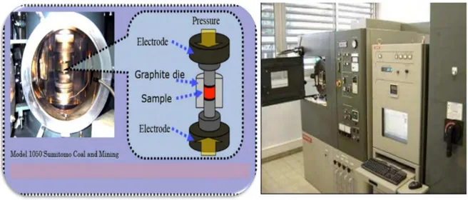
II.2.3. Elaboration of dense ceramics ... 57
II.2.4. Conventional sintering ... 60
II.3. Analyses techniques ... 60
II.3.1. Analysis of chemical compositions by X-ray fluorescence (XRF) ... 60
II.3.2. Analysis of crystalline structure by X-ray diffraction (XRD) ... 61
II.3.3. Microstructural analysis by Field Emission Gun Scanning Electron Microscope (FEG-SEM) ... 64
II.3.4. Thermal gravimetric analysis (TGA) ... 66
II.3.5. Thermal mechanical analysis (TMA) or dilatometry ... 67
II.3.8. Electrical properties of the thin films ... 72
II.4. References ... 73
CHAPTER III ... 75
FIRST-PRINCIPLES ELECTRONIC STRUCTURE CALCULATIONS FOR THE WHOLE SPINEL OXIDE SOLID SOLUTION RANGE MnxCo3-xO4 (0 ≤ x ≤ 3) ... 75
III.1. Introduction ... 77
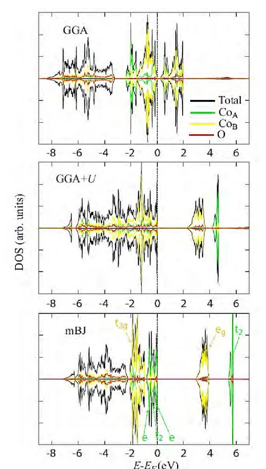
III.2. Atomic, magnetic and electronic structures of Mn and Co spinel oxides ... 78
III.2.1. Co3O4 ... 78 III.2.2. Mn3O4 ... 81 III.2.3. MnxCo3-xO4 ... 86 III.3. Conclusion ... 98 III.4. References ... 100 CHAPTER IV ... 107
SYNTHESIS AND CHARACTERIZATION OF POWDERS AND THIN FILMS OF SPINEL OXIDES MxCo2-xMnO4 (M = Ni, Cu, Zn; x = 0, 0.15, 0.30, 0.60) ... 107
IV.1. Introduction ... 109
IV.2. Synthesis and characterization of the powders ... 110
IV.2.1. Synthesis ... 110
IV.2.2. Characterization of the powders ... 112
IV.3. Preparation and characterization of thin films ... 130
IV.3.1. Stabilization of colloidal dispersion ... 131
IV.3.2. Thin films preparation using the dip-coating technique ... 132
IV.3.3. Characterization of thin films ... 133
(GI-XRD) ... 137
IV.4.2. Microstructure characterization determined by Field Emission Gun Scanning Electron Microscope (FEG-SEM) ... 142
IV.5. Conclusion ... 146
IV.6. References ... 148
CHAPTER V ... 151
PHYSICAL PROPERTIES OF SPINEL OXIDE THIN FILMS MxCo2-xMnO4 (M = Ni, Cu, Zn; x = 0, 0.15, 0.30, 0.60) AND CHARACTERIZATION OF THIN FILMS PREPARED BY PULSED LASER DEPOSITION ... 151
V.1. Introduction ... 153
V.2. Physical properties of spinel oxide thin films deposited by the dip-coating technique ... 153
V.2.1. Optical properties ... 153
V.2.2. Electrical properties of the spinel oxide thin films ... 172
V.3. Preparation and study of spinel oxide and cuprite thin films deposited by the PLD technique ... 178
V.3.1. Thin films preparation ... 178
V.3.2. Characterization of the oxide thin films deposited by the PLD method ... 179
V.4. Conclusion ... 183
V.5. References ... 185
AALD Atmospheric Atomic Layer Deposition
ASR Area Specific Resistance
AZO Aluminium doped Zinc Oxide CB Conduction Band
CCD Charge Coupled Device
CET Coefficient of Temperature Expansion CIGS Copper Indium Gallium Selenide CIS Copper Indium Selenide
CMOS Complementary Metal Oxide Semiconductor CNG Compressed Natural Gas
CSD Chemical Solution Deposition CZTS Copper Zinc Tin Sulfide DFT Density Function Theory DOS Density Of States
DSSC Dye Sensitized Solar Cells EQE External Quantum Efficiency
FEG-SEM Field Emission Gun Scanning Electron Microscope FTO Fluorine doped Tin Oxide
FWHM Full Width at Half Maximum
GI-XRD Grazing Incidence X-Ray Diffraction HTM Hold Transport Material
ICP-AES Induced Coupled Plasma Atomic Emission Spectrometry IQE Internal Quantum Efficiencies
ITO Indium Tin Oxide
MOS Metal Oxide Semiconductor
P25 Degussa, average size equal to 25 nm of TiO2
PES Photoemission Spectroscopy PLD Pulsed Laser Deposition PLZT (Pb, La)(Zr, Ti)O3
PMMA Polymethylmethacrylate PSCs Perovskite Solar Cells PV Photovoltaic
SPS Spark Plasma Sintering
TCOs Transparent Conducting Oxides
TGA Thermal Gravimetric Analysis TMA Thermal Mechanical Analysis
UPS Ultraviolet Photoelectron Spectroscopy UV-VIS-NIR Ultraviolet Visible Near Infrared VASP Vienna Ab initio Simulation Package VB Valence Band
XPS X-ray Photoelectron Spectroscopy XRD X-Ray Diffraction
General introduction
The development of societies across the world and increase in energy consumption show that we will require more energy in the future. In the context of energy crisis, climate change, long-term supply and security, solar energy is an attractive source. It is plentiful, virtually inexhaustible and can provide more than enough energy to our society. However, the issue with producing electricity and fuels from solar energy is that it is still expensive, primarily from the materials used in building the cells.
Metal oxide semiconductors are an attractive class of materials that are extremely low cost and can be produced at the scale needed to meet widespread demand. The synthesis and studies of nanosized materials have been intensively pursued in the recent years not only because of their characterization interest but also for their interesting properties such as catalytic, thermal, magnetic, electrical and optical properties and the variety of applications related to them. In the recent years, various methods have been developed for the preparation of nanostructured spinel oxides: physical and chemical vapor depositions, soft-chemistry methods, etc… The spinel structure is an important class of materials and metal oxide based spinels exhibit very interesting properties for uses in sensors, fuel cells, catalysis, solar cells, transformers, etc.
We wish to develop further a young thematic at the CIRIMAT based on the search for new inorganic materials, including spinel oxides, that can be integrated in solar cells. Researchers around the globe are racing to develop efficient thin film solar cells. Besides the Si and CuInSe2 main families of inorganic semiconductor materials for solar cell applications,
CdTe and GaAs are also important. However, indirect band gap energies (for Si), scarcity and/or toxicity of elements, and expensive ways of production are restricting factors for mass production of such type of solar cells. Thus, simultaneously to the search for solar cell efficiency improvements, it is necessary to find new compounds with suitable semiconducting properties in order to open new horizons for lower cost cells. Metal oxide based solar cells have the potential to counteract all the difficulties encountered in the usual solar cells. The all-oxide photovoltaic approach is very attractive due to the chemical stability, negligible toxicity and abundance of many metal oxides that potentially allow manufacturing of solar cells under ambient conditions. Metal oxides are widely used as components in photovoltaic cells such as
transparent conducting front electrodes or electron-transport layers, while only very few metal oxides have been used as light absorbers, basically p-type Cu2O.
It is proposed here to synthesize by soft-chemistry routes and study nanoparticles and powders of new semiconductor and light absorber spinel oxides, with controlled size and morphology, for processing as thin films that could be easily integrated in an energetic system of conversion. Various doping schemes will drive to suitable physical characteristics such as the energy gap, sunlight absorption and charge transport for different applications, firstly for photovoltaics. The new semiconductors will be processed into thin layers for being used in simple photovoltaic cells with the ambition of preparing a complete solid oxide solar cell and replacing Si-based solar cells thanks to higher performances and lower production costs.
Therefore, the main objective of this thesis is to develop and study new photon-absorbing oxide materials based on the spinel structure with semiconducting properties. Our study focuses on Metal-doped MnCo2O4 spinel oxides (with Metal = Ni, Zn or Cu), since the
reference material MnCo2O4 exhibits good electrical p-type semi-conductivity and sun light
absorbance, while trying to improve these properties thanks to doping.
A large description of the world energy resources, the main families of inorganic materials usually found in thin film solar cells, the future and promising alternative of photovoltaics and the main features of spinel metal oxides that can be integrated in solar cells will be done in the first chapter. The second chapter will present all the experimental procedures and systems used during this work to prepare and characterize our materials. Chapter III presents first-principles calculations performed over the whole solid solution range of manganese and cobalt spinel oxides aimed at determining their density of states and electronic band structure, through a collaborative work with the essential contribution of an academic partner. In chapter IV, a full description of the synthesis method used to prepare nanopowders of metal spinel oxides, with controlled size and morphology, is given. Various characterization techniques were used in order to address the (micro-)structural properties of nano materials obtained at low temperature (T < 120 °C). Colloidal dispersions were also stabilized in order to prepare oxide thin films at room temperature without complexing agent. Their structural properties were characterized in details at room and high temperatures on various substrates, essentially by means of X-ray diffraction and electron microscopy. Finally, chapter V presents the optical and electrical transport measurements performed at different temperatures on the
Metal-doped MnCo2O4 spinel oxides prepared to increase the film compactness and density, as
well as its electrical conductivity. The energy band gaps were also determined for each compound. Thin films light absorption and electrical conductivity were studied in detail in order to incorporate these materials into existing or especially designed types of solar cells in the near future. A study based on thin film preparation of Cu2O and pure MnCo2O4 obtained by using
CHAPTER I
I.1. Introduction
The world energy demands are based on limited natural resources. These natural resources are harder to reach and can take hundreds of thousand years to replenish while the world demands are increasing with the expected 9.7 billion population growth from now to 2050. Global warming and climate change refer to an increase in average global temperatures. Moreover, the burning of fossil fuels releases greenhouse gases such as CO2 or COx and also
NOx, SOx …which causes air pollution to the atmosphere.
The main reason for international energy crisis in the 1970s was due to a lack of oil procurement in major industrial nations such as Germany, France, the United States, Canada, and other main developed countries. More recently, fuel protests in the United Kingdom (UK) in 2000 were caused by a rise in the price of crude oil combined with already relatively high taxation on road fuel in the UK. North American natural gas crisis occurred from 2000 to 2008. Central Asia energy crisis in 2008 was caused by abnormally cold temperatures and low water levels in an area dependent on hydroelectric power. At the same time, the South African President was appeasing fears of a prolonged electricity crisis in his country. China experienced severe energy shortages towards the end of 2005 and again in early 2008. During the latter crisis they suffered severe damage to power networks along with diesel and coal shortages. Supplies of electricity in Guangdong province, the manufacturing hub of China, were predicted to fall short by an estimated 10 GW. In 2011, China was forecast to have a second quarter electrical power deficit of 44.85 - 49.85 GW [1].
Alternative resources are thus necessary and renewable energies, including solar cells, which can provide enough energy to the world should now be a priority.
I.1.1. Decreases in fossil fuels reserves
Fossil fuels are created within the earth’s crust, over extended periods of time, due to the extreme pressure applied to fossilized plants, animals and other organisms. Fossil fuels include coal, oil, and natural gas. Fossil fuels play a crucial role in the world energy market.
Figure I. 1: Energy obtainable from fossil fuels as a function of time (a) and comparison of the world energy consumption to the total energy supplied by fossil fuels (b) [2].
Figure I. 1 shows the energy obtainable from fossil fuels as a function of time and the world energy consumption compared to the total energy supplied by fossil fuels. Since 1900, the consumption of fossil fuels has nearly doubled every 20 years (Figure I. 1a). It is obvious that current use of fossil fuels continues threatening global stability and sustainability. This problem is even further compounded by increasing world population, rapid technological development, increasing energy requirements. With the rapid increase of world energy demand and energy consumption (Figure I. 1b), the fossil fuels energy cannot be considered as the principal energy sources in the future.
I.1.2. Climate change and global warming
Climate change is a change in the statistical distribution of weather patterns when that change lasts for an extended period of time (i.e., decades to millions of years). Climate change may refer to a change in average weather conditions, or in the time variation of weather around longer-term average condition. The primary cause of climate change is the burning of fossil fuels, such as oil and coal, which emits greenhouse gases into the atmosphere, primarily carbon dioxide.
Figure I. 2: The annual greenhouse gas emission by sector [3].
Global warming is caused by greenhouse effect. Greenhouse gases in the atmosphere act like a mirror and reflect back to the Earth a part of the heat radiation, which would otherwise be lost into space. The higher the concentration of greenhouse gases in the atmosphere, the more heat energy is being reflected back to the Earth. As shows in Figure I. 2, the major greenhouse gases emission comes from the fossil fuels.
Evidence for a warming world comes from multiple independent climate indicators, from high up in the atmosphere to the depths of the oceans. They include changes in surface, atmospheric and oceanic temperatures, glaciers, snow cover, sea ice, sea level and atmospheric water vapor. Scientists from all over the world have independently verified this evidence many times [4, 5].
In the context of the present energy crisis and global warming, we need to develop energy generation techniques that support the requirements of sustainability and renewability. The production and use of renewable energy sources needs to be largely improved in order to provide sufficient energy to Humanity and to protect our Environment.
I.2. Renewable energy: Energy of the future
Renewable energy is any energy source that is replaced rapidly by a natural process and virtually inexhaustible, such as sunshine, wind, flowing water, biological processes and geothermal heat flows. Renewable energy sources may be used directly or to create other more convenient forms of energy. Examples of direct use are solar ovens, geothermal heating and windmills. Examples of indirect use, which require energy harvesting, are electricity generation through wind turbines or photovoltaic cells or production of fuels such as ethanol from biomass [6]. Renewable energy sources also are friendly with the environment, economic and are sustainable. However, they have some disadvantages and drawbacks, some of which are intrinsic or due to the status of technology development.
There are many sources of energy that are renewable, considered to be environmentally friendly and harness natural processes. Tidal power, wave power and hot hydrogen fusion are sources that can be used to generate electricity. However, each of these suffers from one or another significant drawback and cannot be relied upon at this time to solve the upcoming energy crunch. Among the most reliable renewable energy sources are wind power, hydroelectric energy, biomass energy, geothermal energy and solar energy.
I.2.1. Wind power
Wind power is the conversion of wind energy by wind turbines into a useful form, such as electricity or mechanical energy. The blades of the windmill are attached to a turbine that turns the kinetic energy (energy of movement) into electricity. Countries that have an abundance of empty land and high wind speeds have been able to utilize this renewable source of energy to fill in the gap between demand and supply from traditional means of energy. For example, France has the third largest wind resources in Europe with a 10358 MW total installed capacity in 2015 from 910 wind farms [7]. Wind power tower can be found singularly, but
usually many together in wind farms. Manufacture and implementation of wind farms can be costly and some local people object to on-shore wind farms, arguing that it spoils the countryside. Figure I. 3 shows the wind farm and wind power schematic.
Figure I. 3: Wind farm and wind power schematic.
I.2.2. Hydroelectric energy
Hydroelectricity is electricity produced from the energy of falling water or fast running water. In the late 1800's, hydro-power became a feasible method for generating electricity. Decent-sized bodies of water, such as streams or rivers with high elevation drops and high currents are the best candidates for hydro power. The current provides substantial energy, which is harvested when water pushes through the paddles of an installed turbine, creating mechanical energy. If connected to an electrical generator, the water-powered turbine will spin the generator, converting mechanical energy into electrical energy. The first commercial hydroelectric power plant was built at Niagara Falls in 1879. Hydroelectric power provides about 20 % of the world's electricity. Hydropower has seen a recent jump in popularity with the World Bank naming it as one viable solution to keep up with growing energy demands while simultaneously avoiding carbon and carbon emissions into the atmosphere. Figure I. 4 shows the dam and schematic of hydropower.
Figure I. 4: Dam hydropower images.
I.2.3. Biomass energy
Biomass energy is obtained from combusting or decomposing organic matter. Types of biomass are obtained from plants, plant waste and crops, landfills, municipal and industrial waste, trees and agricultural waste making them ‘biological’ in nature. Biogas has been produced in natural circumstances for thousands of years. It is only recently that we have been able to produce it in controlled conditions and compress it to make Compressed Natural Gas (CNG). Biofuels are basically ethanol, which is made when sugar is fermented. Similarly for CNG, this alcohol substance that is normally blended with gasoline as a form of car fuel, is used in the transportation sector. Figure I. 5 presents the converting biomass sources into energy.
I.2.4. Geothermal energy
Geothermal energy is a very powerful and efficient way to extract a renewable energy from the Earth through natural processes. Within the Earth, there is a great deal of energy trapped inside molten magma. All of this heat moves to the deep stores of water and air that flow through the Earth. In order to release the heat and regulate the temperature of the core, the heated water and air are released through vents, which are seen as holes in the crust of the Earth. The vents of heated air and steam are used to generate power which is yet another renewable source of energy. Geothermal energy is completely renewable, reduces dependence on fossil fuels, provides job benefits and significant cost saving. Figure I. 6 presents a diagram of geothermal power plant.
Figure I. 6: Diagram of geothermal power plant.
I.2.5. Solar energy
The primary source of energy is sunlight. Solar energy is used by plants in the process of photosynthesis. It is the reason why life on the planet Earth has flourished. About 70 % of sunlight gets reflected back into the space and only 30 % of sunlight is enough to meet up our energy demands. This source of energy relies on the nuclear fusion power from the core of the Sun. It can be collected and converted in a few different ways. One example is solar heaters. Whether it is industrial grade water heating or simple heating to cook food, solar energy can be utilized quite easily. With the development of solar panels and photovoltaic cells, it can also be used to create and store energy as needed. Solar powered homes, cars and appliances are
becoming common these days, as are solar farms that provide electricity to areas that are not on the grid. Solar cells are becoming more efficient, transportable and even flexible, allowing for easy installation. Two types of solar energy production are presented in Figure I. 7.
Figure I. 7: Solar energy production.
This thesis is mainly concerned primarily with renewable energy from the sun, which can product electrical energy by using the photovoltaic effect. In the next section, the different generations of photovoltaic cells will be presented.
I.3. Most familiar generations of photovoltaic cells
A solar cell or photovoltaic cell is an electrical device that converts the energy of light (photons) directly into electricity (voltage) by the photovoltaic effect. This effect was first noted by a French physicist, Edmond Becquerel, in 1839. He first observed the photovoltaic effect by using an electrode of platinum covered with a thin layer of light sensitive material such as silver chloride. He was able to demonstrate that the current was not due to a heating effect and obtained a rough spectral response curve by means of color filters placed between the electrode and the light source, which was the sun. In addition, he postulated that the current resulted from a chemical reaction at the electrode and gave the correct reaction [8]. In 1905, Albert Einstein described the nature of light and the photoelectric effect, for which he later won a Nobel Prize in physics. The first photovoltaic module made of silicon was built by Bell Laboratories in 1954. Throughout the 1960s, photovoltaic cells were primarily used to provide electrical power
for earth-orbiting satellites. In the 1970s, improvements in manufacturing, performance and quality of photovoltaic modules helped to reduce the cost. This opened up a number of opportunities for powering remote terrestrial applications, including battery charging for navigational aids, signals, telecommunications equipment and other critical, low-power needs. In the 1980s, photovoltaic cells became a popular power source for consumer electronic devices, including calculators, watches, radios, lanterns and other small battery charging applications. Following the energy crises of the 1970s, significant efforts also began to develop photovoltaic power systems for residential and commercial uses, both for stand alone, remote power and utility connected applications. During the same period, international applications for photovoltaic systems to power rural health clinics, refrigeration, water pumping, telecommunications, and off-grid households increased drastically; it remains a major portion of the present world market for photovoltaic products. Today, the industry’s production of photovoltaic modules is growing at approximately 25 percent annually and major programs in the United States, Japan and Europe are rapidly accelerating the implementation of photovoltaic systems on buildings and interconnection to utility networks.
I.3.1. First generation of photovoltaic cells
The first generation includes cells consisting of silicon (or germanium) doped with boron (p-type) and phosphorus (n-type) in a pn junction (see Figure I. 8). This generation is dominating the commercial market. Silicon cells have a quite high efficiency, but very pure silicon is needed. Due to the energy requiring process, the price is too high compared to the power output. Also, silicon possesses an indirect band gap and thicker cells are required in order to compensate for the energy loss (mainly as heat). The first generation solar cells are produced on wafers. Each wafer can supply 2-3 Watts of power. To increase power, solar modules, which consist of many cells, are used. Generally, there are two types of first generation solar cells. They differ by their crystallization levels. If the whole wafer is only one crystal, it is called a single crystal solar cell. If the wafer consists of crystal grains, it is called a polycrystal solar cell as shown in Figure I. 8. Although efficiency of single crystal solar cells is higher than polycrystal solar cells, production of a polycrystal wafer is easier and cheaper. Polycrystal cells do not go through the cutting process used for single crystal cells. Instead, the silicon is melted and poured into a square mold, hence the square shape of polycrystal. Therefore, they are much
more affordable since a negligible amount of silicon is wasted during the manufacturing process and are more competitive than single crystals.
Figure I. 8: pn-junction and two types of first generation solar cells: single crystal and polycrystal.
I.3.2. Second generation of photovoltaic cells
Second generation photovoltaic cells are usually called thin film solar cells. They are made from layers of semiconductor materials only a few micrometers in thickness such as cadmium telluride/cadmium sulfide (CdTe)/CdS, copper indium selenide (CIS) or copper indium gallium selenide (CIGS), copper zinc tin sulfide (CZTS) and gallium arsenide (GaAs). Since the second generation solar cells avoid use of silicon wafers and have a lower material consumption thanks to direct band gaps, it has been possible to reduce production costs. These thin films can also be grown on flexible substrates. So, second generation solar cells are
applicable on textile products or on foldable devices. While many variations of thin film products exist, they typically achieve efficiencies of 7-13 % [9, 10]. However, a lot of research and development is being put into thin film technologies and many scientists suspect efficiencies to climb as high as 23.3 % in coming models (see Figure I. 9).
Figure I. 9: Current status of photovoltaic cells and their efficiency [11].
Another perk is that high heat and shading have less of a negative impact on thin film technologies. For these reasons, the thin film market continues to grow. Figure I. 10 shows example of major systems of thin films solar cells.
Thin film solar cells such as CIGS/CdS or CdTe/CdS are particularly studied for improving efficiency. Since CdTe has an optimal band gap of 1.49 eV for single junction
devices, efficiencies above 20 % should be achievable in the commercial CdTe solar cells [12]. Contreras et al. (2005) presented several devices with an energy conversion efficiency of 19.5 % for CIGS (with band gap of 1.14 eV) thin film solar cells [13]. But there are some drawbacks for this type of solar cells as Te is not abundant and Cd is toxic. More recently, copper zinc tin sulfide (CZTS) with a kesterite structure (CZTS/CdS – see Figure I. 10), is considered to be an alternative material to the CIGS which is currently under extensive development. CZTS is assumed to be analogous to CIGS when In (III) is replaced by Zn (II), Ga (III) is replaced by Sn (IV) and Se (VI) by S (VI). For the CZTS, the high absorption coefficient (104 cm-1) and optimum band gap (1.0 – 1.5 eV) cover the maximum solar spectrum
and open a gateway for economic and ecological thin film devices fabrication. The highest efficiency (12.6 %) was reported using hydrazine based non-vacuum particle solution approach [14-16].
Figure I. 10: Schematic of thin film solar cells systems [14, 17].
I.3.3. Third generation of photovoltaic cells
Third generation photovoltaic cells are novel technologies which are promising but not commercially proven yet. Most developed third generation solar cell types are nanocrystal based solar cells, polymer based solar cells, dye sensitized solar cells (DSSC) and concentrated solar cells. DSSC are based on dye molecules between electrodes that create electron/hole pairs (excitons) after absorbing light and transferring electrons to n-type conductive TiO2
nanoparticles. An electrolyte based on iodine is necessary to refurbish the valence band of the light absorber dye. The structure of a dye-sensitized photovoltaic cell is shown in Figure I. 11.
Figure I. 11: Structure of a dye-sensitized solar cell [18].
Their production is easy with respect to other technologies. DSSC can be of various colors and is still efficient under small illumination. Michael Graetzel, the original DSCC designer, recently announced the fabrication of solid state DSSC with 15.0 % power conversion efficiency, by the means of PbI2 firstly introduced from solution into a nanoporous TiO2 film
and subsequently transformed into the perovskite by exposing it to a solution CH3NH3PbI3 [19].
Concentrated photovoltaic cell is another promising technology. The main principle of a concentrated cell is to concentrate large amounts of solar radiations onto a small region where the photovoltaic cell is located. These cells are typically applied in the concentrator modules based on a concept of the small-aperture refractive concentrators. Figure I. 12 shows a schematic of a concentrated photovoltaic cell system. The amount of semiconductor material, which might be very expensive, is reduced in this way. In this system a perfect optical system should be integrated. Concentration levels start from ten suns to thousand suns. Their total cost can be lower than for conventional systems. Concentrated photovoltaic cells are thus promising technologies for the near future.
Figure I. 12: Schematic of a concentrated photovoltaic cell.
I.4. Metal Oxide semiconductors for photovoltaic cells
I.4.1. n-type wide band gap metal oxides
Wide band gap metal oxides are electrically conductive materials with a comparably low absorption of visible light (from 380 nm to 780 nm of wavelength) and with an optical band gap usually greater than 3.2 eV. n-type metal oxide semiconductors are widely used as components in photovoltaic cells and modules, either as transparent conducting front electrodes, as electron (and hole) transport layers that provide the required charge selectivity between absorber and the contacts, or as back electrodes [20, 21]. Among the most popular transparent conducting front electrodes used for electronic devices are the so-called transparent conducting oxides (TCOs) such as fluorine doped tin oxide (FTO), indium tin oxide (ITO) or aluminium doped zinc oxide (AZO) [22]. Wide band gap metal oxides for electron conducting layers such as TiO2, ZnO, SnO2 are also n-type metal oxides. For instance, ZnO and AZO are
used as electron transport layers for the top and front electrodes, respectively, in thin film Cu(In, Ga)Se2 (CIGS) solar cells [17, 23]. Compact thin films of ZnO and TiO2 have been used
in polymer based thin film solar cells to achieve a selective contact [24, 25]. In organic solar cells, hole transport materials such as V2O5, WO3, MoO3 and NiO were used for hole-injection,
hole-extraction interlayers, charge generation and charge recombination layers [26, 27].
The electrical conductivity of wide band gap metal oxides can be explained by the band theory of semiconductors. When atoms come together to form a compound, their atom orbital energies mix to form molecular orbital energies. As more atoms begin to mix and more molecular orbitals are formed, it is expected that many of these energy levels will start to be very close to, or even completely degenerate, in energy. These energy levels are then said to form bands of energy. Electrons occupy the lowest energy orbitals and electrons in bulk materials fill the bands starting at the lowest energy. The energy gap between the highest energy level of electron-occupation with the next available energy level provide a means for understanding the electrical conductivity of a material. Electrons carry a current by moving through a material, and this motion can be thought of in terms of electrons moving from one orbital to another. But electrons within a filled band cannot move readily to conduct electricity. To have mobile electrons, we will need to have an unfilled band or portion of a band that is close in energy to a filled band or portion of a band. Diagrams of energy bands for solids are shown in Figure I. 13.
Figure I. 13: Diagrams of energy bands for different solids
For the large energy gap between the valence and conduction bands in an insulator, at ordinary temperatures, no electrons can reach the conduction band. In semiconductors, the band gap is small enough that so thermal energy can bridge the gap for a small fraction of the electrons. The highest filled energy level is at the top of the valence band, but the next band is only modestly higher in energy. In semiconductors, some electrons have enough thermal energy to reach the upper band even at room temperature, and therefore they present limited electrical
conductivity. If the temperature is increased, more electrons should occupy the upper band, and the conductivity of semiconductors increases at higher temperatures. In conductors, there is no band gap since the valence band overlaps the conduction band (or consist of an unfilled valence band). The energy below which an energy level is likely to be filled is called the Fermi level [28].
I.4.1.2. Optical properties of n-type metal oxide semiconductors
Optical properties of wide band gap (greater than 3.2 eV) metal oxides thin films usually exhibit transparency in visible and near infrared regions of wavelengths and are reflective to thermal infrared radiation. For long wavelengths, wide band gap metal oxides are reflective due to free electrons in the conduction band and for very low wavelengths, absorption is observed due to the band gap of the material [20, 29, 30].
The most striking feature of band gap absorption in wide band gap metal oxides is a strong blue-shift of the determined band gap for increasing doping. N-type semiconductors are materials in which charge carriers are electrons in the conduction band, while p-type materials present electrical current carried by holes in the valence band.
I.4.2. p-type metal oxide light absorbers
Generally, solar cells are built from different main elements (as shown in section I.3).
Besides their electrical properties, it also has to fulfill essential optical requirements. In a typical
n-transparent/p-absorber solar cell, p-type and n-type are put side by side and a pn-junction is
formed. Figure I. 14 shows a simplified illustration of a pn-junction. When light goes on the
p layer where most of the absorption takes place, they transfer energy to some valence electrons,
promote them to higher energy levels; from the lower energy valence bands to higher energy, i.e. excited states of the conduction bands. When the pn-junction is formed, some electrons in the intermediate region are attracted from the n side to combine with holes on the nearby p side. Charge builds up as electrons and holes combine at the pn-junction and excess charges create an electric field. Direct band gaps are a good choice because in a direct band gap semiconductor, the top of the valence band and the bottom of the conduction band occur at the same value of momentum. Therefore, the electron does not need to be given very much momentum to produce
an electron-hole pair. And in the recombination process of electrons and holes to produce photons, the efficiency for a direct band gap is higher. The absorbed photons create electron/hole pairs. Then electric field of the pn-junction separates them and directs them in opposite directions to the electric contacts. It is particularly important to ensure a reasonable transport of the photo-generated minority charge carriers because they dominate the electric behavior of the pn-junction. In most semiconductors the mobility is higher for electrons than for holes, the latter carried by the absorber of p-type conduction [31, 32].
Figure I. 14: pn - junction and electric field inside photovoltaic cells.
For all-oxide photovoltaic cells, the metal oxide absorbing semiconductors should have
a direct band gap, high absorption coefficient in the relevant energy range for photovoltaics (105 cm-1), with most of sunlight absorbed within a small range beneath the surface, and offer
the possibility to fabricate thin films.
Optical characterization is important for p-type oxide semiconductors to be applied in photovoltaic cells. When a radiant flux is incident upon a material surface, three processes occur: transmission, absorption, and reflection. Application of conservation of energy leads to the statement that the sum of the transmission, reflection, and absorption of the incident flux is equal to unity (and in the absence of nonlinear effects) [33]. Measurements of the power reflection, transmission or absorption are the simplest and most direct methods of semiconductor materials spectroscopic analyses. The measurements are simple to perform as long as a satisfactory spectroscopic apparatus is available in the wavelength region of interest.
I.5. All-oxide photovoltaics: The next generation of photovoltaic cells?
The market for photovoltaic cells has grown exponentially over the last few years to fulfil the global energy demand. But, one of the primary challenges to the full-scale implementation of solar energy remains the expensive cost associated with the construction of photovoltaic modules and certain toxic elements in some thin film solar cells. To reach grid parity, further price reductions for photovoltaic systems are required; this call for continued up scaling of the production processes or for uses of novel materials for photovoltaic cells based on high efficiency and cheap materials in combination with low cost deposition methods. Metal oxide semiconductors are very attractive to achieve this goal, many of them show great chemical stability, negligible toxicity, abundance, fulfil the requirements for low cost manufacturing methods at ambient conditions, and could show high conversion efficiency for photovoltaic. A schematic of an all-oxide photovoltaic cell is shown in Figure I. 15. The usual design for such cell, like in many previous generations, consists of a glass substrate, a transparent conductive oxide layer (n-type semiconductor), a metal oxide light absorber (p-type semiconductor) and contact layers (see Figure I. 15).
I.5.1. Cu2O based “all-oxide” photovoltaics
Cu2O, of cuprite structure, is a semiconductor with a direct energy band gap of about
2.2 eV [35, 36]. It is the most investigated metal oxide used as the light absorber for photovoltaics and it has a theoretical limit of energy conversion efficiency of about 20 % under AM1 (air mass at the surface of Earth at noon) solar illumination [37]. Heterojunction devices were developed, mainly with the wide band gap ZnO as an intrinsic n-type semiconductor and cuprous Cu2O as the p-type absorber. Previous attempts to nanostructure Cu2O/ZnO solar cells
required prohibitively long fabrication times or resulted in efficiencies of less than 0.1 % [38, 39]. Hsueh et al. (2007) sputtered Cu2O onto ZnO nanowires grown by a vapor-liquid-solid
technique [39], and Yuhas et al. (2009) drop-cast Cu2O nanoparticles into a hydrothermally
grown ZnO nanowire array with a 10 nm TiO2 coating [38]. Then, the power conversion
efficiency of 1.43 % was improved under air mass 1.5 illumination for photovoltaic device
based on a FTO/ZnO/Cu2O/Au heterojunction structure, which was deposited from a
pH-adjusted electrolyte of LiOH by Kazuya el al. (2013) [40]. 1.46 % and 0,49 V are the power conversion efficiency and open-circuit voltage, respectively, which were achieved for ZnO/Cu2O heterojunctions deposited by atmospheric atomic layer deposition (AALD)
technique [41].
In Cu2O-based heterojunction solar cells, various compounds were used to dope ZnO
used as the n-type oxide thin-film layer to increase the power conversion efficiency. Heterojunctions of ITO/ Zn0.79Mg0.21O/Cu2O showed a power conversion efficiency of 2.2 %,
which were prepared by AALD method [41]. Tadatsugu et al. (2011) reported low cost Al-doped ZnO (AZO)/non-doped ZnO (ZO)/Cu2O heterojunction solar cells with a high
conversion efficiency of 3.83 %, that was fabricated by depositing thin films at a low temperature on thermally oxidized copper sheets using a PLD (Pulsed laser deposition) method [42]. One year later, a high conversion efficiency 4.08 % was obtained with the same AZO/ZnO/Cu2O heterojunction solar cells fabricated by inserting the buffer layer on low cost,
nontoxic Cu2O sheets prepared by thermally oxidizing Cu sheets [43]. In January 2016, the
same group of Tadatsugu published the highest conversion efficiency (over 6 %) for an open circuit voltage of Cu2O-based heterojunction solar cells so far using multicomponent oxide thin
films as the n-type semiconductor layer as shown in Table I. 1 [44]. The obtained improvement of photovoltaic properties may be attributable mainly to an increase of the barrier height formed in the p-n junction, resulting from the inserted buffer layer functioning as an n-type ZnO layer
as well as an enhancement of carrier lifetimes near the interface between the non-doped ZnO thin-film buffer layer and the Cu2O.
Table I. 1: Conversion efficiency and open circuit voltage of Cu2O-based heterojunction solar
cells using multicomponent oxides as the n-type oxide semiconductor thin film layer [44].
Heterojunction solar cell Conversion efficiency (%) Circuit voltage (V)
AZO/ZnGa2O4/Cu2O 5.38 0.81
AZO/Zn2SnO4/Cu2O 3.64 0.63
AZO/(Ga0.975Al0.025)2O3/Cu2O 5.42 0.84
AZO/(Zn0.91Mg0.09)2O3/Cu2O 4.29 0.80
MgF2/AZO/AGMZO/Cu2O:Na 5.40 0.96
MgF2/AZO/(Ga0.975Al0.025)2O3/Cu2O:Na 6.25 0.84
* AZO: Al doped ZnO; AGMZO: Al-Ga-Mg-Zn-O multicomponent oxides, composed of Al 2O3,
Ga2O3, MgO and ZnO.
Besides ZnO, other metal oxides have been used to form bilayer heterojunction all-oxide photovoltaic cells such as TiO2 and ITO. Sahrul et al. (2013) prepared a TiO2/Cu2O
heterojunction solar cell, which was employing polymer electrolyte (containing Li+ ion) with a power conversion efficiency of 1.05 % [45]. Luo et al. (2012) synthesized TiO2 by a
hydrothermal reaction and Cu2O thin films are then electrodeposited at the surface of TiO2
nanorods. The efficiency of the resulting TiO2/Cu2O nanorods radial heterojunction solar cells
is up to 1.25 % [46]. Mitiga et al. (2006) reported the power conversion efficiency of 1.07 % and 2.01 % obtained for MgF2/ITO/Cu2O and MgF2/ITO/ZnO/Cu2O heterojunction solar cells,
respectively, which were made by deposition of transparent conducting oxide (TCO) films on Cu2O substrates. The TCO films have been grown by ion beam sputtering on good quality Cu2O
I.5.2. Perovskite solar cells (PSCs)
Perovskite are materials with ABX3 stoichiometry (for example, calcium titanate
CaTiO3) that form crystal structures where B cations reside in the centers of corner-shared
octahedral of X anions, with the A cation filling the resulting interstices. Perovskite have captivated researchers with properties such as superconductivity, ferroelectricity, piezoelectricity, ferromagnetism and antiferromagnetism. Perovskite solar cells (PSCs) have received considerable attention in recent years as a promising material capable of developing high performance photovoltaic devices at a low cost. Even though most of the known perovskites are metal oxides, metal halide perovskites have recently been taking the field by storm with their record shattering photovoltaic performance combined with low-cost processing methods and earth-abundant elemental compositions.
Figure I. 16: Progress of power conversion efficiency of the perovskite solar cells and flexible perovskite solar cells devices in the past 6 years[48].
The best solar cell performance has been obtained from hybrid organic-inorganic metal halide perovskites such as methylammonium lead iodide (CH3NH3PbI3) or methylammonium
lead bromide (CH3NH3PbBr3). Figure I. 16 shows the progress in the perovskite solar cells
which have jumped from 3.8 % of methylammonium lead halide CH3NH3PbX3 (X = Br, I)
sensitized liquid solar cells in 2009 [49], to more than 20 % of formamidinium lead iodide (NH2CHNH2PbI3) solar cells in 2015 [48]. Qin et al. (2014) presented a device structure
consisting of titanium dioxide as a scaffold as well as electron collector, lead halide perovskite as the light harvester and CuSCN as the hold transport material (HTM) with high power conversion efficiency of 12.4 % under full sun illumination [50].
Recently, ferroelectric perovskite oxides have also drawn much attention due to potential applications in the field of solar energy. When a ferroelectric material is illuminated with light, charge carriers (electron-hole pairs) are generated. These photo-generated carriers are separated and driven to the electrodes by the polarization induced internal electric field, causing a photovoltaic output. The photovoltaic effect in ferroelectrics is a bulk-based effect, which differs from the junction based semiconductor photovoltaic effect. Since the internal electric field is not limited to an interfacial region in a ferroelectric, photovoltaic responses can be generated without forming complex junction structures. Figure I. 17 shows a simplified schematic of photovoltaic mechanism in a ferroelectric material.
Figure I. 17: Simplified schematics for the interfacial photovoltaic effect in a semiconductor p-n junction (left) and the bulk PV effect in a ferroelectric thin film (right).
Some ferroelectric materials for photovoltaics, such as BiFeO3 (BFO), Pb(Zr,Ti)O3
(PZT) and (Pb,La)(Zr,Ti)O3 (PLZT), are here briefly reviewed:
BFO is a promising material with low band gap energy (2.3 < Eg < 2.8 eV) [51],
and high remnant polarization (50 – 150 µC.cm-2) [52, 53]. Heterostructures of ITO/BFO/SRO (SrRuO3) are characterized by large VOC ~ 0.8 – 0.9 V and
external quantum efficiency (EQE) ~ 10 % [51].
PZT has occupied a significant place in the ferroelectric photovoltaic world due to improved photovoltaic efficiency. An efficiency of 1.25 % is reported in PZT
thin films when they are grown on n-type Si for heterojunction Ag/n-a-Si/PZT/ITO/glass [54].
PLZT is another class of ferroelectric material which is being studied for photovoltaic properties. One of the early work investigating the photovoltaic responses was based on ceramic of Pb0.97La0.03Zr0.52Ti0.48O3 (PLZT - 3/52/48)
composition [55]. Poosanaas et al. (1999) investigated the maximum photocurrent of PLZT - 4/48/52 composition which is in the tetragonal phase while the maximum photovoltage was found at PLZT - 5/54/46 which is close to the morphotropic phase boundary of the PLZT phase diagram [56]. Unprecedented high photovoltaic power conversion efficiency around 0.28 % was achieved with epitaxial PLZT – 3/52/48 ferroelectric thin films [57].
I.5.3. Spinel oxide solar cells
Recently, many spinel oxides of AB2O4 were investigated as a light absorbers for
all-oxide thin film photovoltaic cells because of their nearly ideal optical band gap of around 1.5 eV, which could reach 40 % of the theoretical conversion efficiency [37].
There is strong research attention on heterojunctions of spinel oxides for inorganic solar cells such as TiO2/Co3O4 where Co3O4 is a p-type semiconductor, which has two noticeable
direct transitions in the visible range with band gaps energy of 1.45 eV and 2.26 eV [58]. The first J-V curve of TiO2/Co3O4 heterojunction (in Figure I. 18) was measured under conditions
of dark and light by Rühle and his colleagues in 2012 [34], and was detailed in 2015 by the same group [59]. All-oxide solar cells with a multi-layered geometry of glass/FTO/TiO2/(CoxFe1-x)3O4/Au, enhanced photovoltaic performance, with Jsc of 53 µA cm-2
and Voc of 534 mV for samples with Co/(Co + Fe) composition ratio of approximately 55 %
Figure I. 18: Cross section SEM (top) of sprayed TiO2 and Co3O4 thin film deposited at
600 ºC, SEM images of samples at different temperatures and J-V curve of Co3O4/TiO2
heterojunctions when Co3O4 was deposited at different temperatures (bottom) [59].
After the pioneer work on dye-sensitized solar cells (DSSC) by O’Regan and Grätzel in 1991 [61], wide variety of oxide-based semiconductors has been studied as alternative electrode materials of DSSC. These researches focus on the simple replacement of TiO2 for as
double-oxide-based phase pure porous electrode. Some spinel oxides have been examined as photo-anodes for DSSC. Tan et al. (2007) examined zinc stannate (Zn2SnO4) with band gap of 3.6 eV,
and reported the power conversion efficiency of 3.8 %. According to Tan et al., the electron diffusion length for Zn2SnO4 is shorter than P25 (Degussa, average size equal to 25 nm of TiO2)
film. However, photo-current density for a Zn2SnO4 cell was higher than that for a P25 cell with
the same film thickness (~ 6 µm) [62]. Lana-Villarreal et al. (2007) also reported the DSSC performance of Zn2SnO4 DSSC [63]. Mercado et al. (2014) presented ternary substituted (zinc
or nickel) cobalt oxide spinels thin films as a dye-sensitized p-type hole transport support in a photo-electrochemical cell. The highest photocurrent and quantum efficiencies were measured in zinc-cobalt-oxide devices with an internal quantum efficiencies (IQE) of > 90 % and an open circuit voltage of around 260 mV [64].
I.6. Mixed valence spinel oxides as solar absorbers
I.6.1. Crystal structure
The spinel structure is formulated MM'2X4, where M and M' are tetrahedral and
octahedral coordinated cations, respectively, and X is an anion (typically O, S or F). The structure is named after the mineral MgAl2O4, and the compounds from this family have the
general formula AB2O4. Where A and B are either divalent (+2) and trivalent (+3) or tetravalent
(+4) and divalent cations. The crystal structure was determined independently by Bragg [65] and Nishikawa [66]. Figure I. 19 shows Schematic of the spinel structure of MgAl2O4.
Figure I. 19: Schematic of the spinel structure of MgAl2O4 [67].
Cubic spinels have been assigned to the space group Fd3̅m. The unit cell of a spinel consists of eight formula units with the oxygen ions forming a closed-packed faced centered
cubic (fcc) lattice and therefore, may be represented as 8[AB2O4] so it may be represented as
A8B16O32. Within the face-centered cubic lattice formed by 32 oxygen ions two types of
interstitial positions exist, which can be occupied by the metallic cations. There are 64 tetrahedral interstitial sites surrounded by 4 oxygen ions (noted as A site) and 32 octahedral sites surrounded by 6 oxygen ions (noted as B site). In the spinel structure, 8 out of 64 tetrahedral sites and 16 out of 32 octahedral sites are occupied by the cations.
Depending on the occupation and distribution of the cations in the tetrahedral and octahedral sites, spinels can be further classified as normal, inverse and mixed spinels which can be represented by the general formula:
(A1-2xB2x)[A2xB2-2x]O4
Where ( ) represent the tetrahedral sites and [ ] represent the octahedral sites. There are three spinel types with general formula:
Normal spinel: x = 0, the tetrahedral sites are filled with the divalent cations (A2+) and the octahedral site are filled with the trivalent cations [B3+]. It can be represented as:
(A2+)[B23+]O4
Examples: MgAl2O4, ZnFe2O4, ZnCrFeO4, MnAl2O4, Mn3O4, Co3O4
Inverse spinel: x = 0.5, the tetrahedral sites are filled with half of the trivalent cations and the octahedral site are filled with the other half of the trivalent cations and the divalent cations. It can be described as:
(B3+)[A2+B3+]O4
Examples: MgFe2O4, NiFe2O4, CoFe2O4, Fe3O4.
Mixed spinel (random spinel): 0 < x < 0.5, the relocation of cations can cause a change in lattice parameter or a deformed crystal structure [68]. The cations A and B occupied both sites, octahedral and tetrahedral.
Figure I. 20 presents the examples of three spinel types, normal spinel of MgAl2O4 with
all Mg2+ cations positioned in tetrahedral sites while the octahedral sites are filled with Al3+ cations [67]. In inverse spinel of NiFe2O4, Fe3+ cations are distributed equally across tetrahedral
and octahedral sites, while Ni+2 cations occupy octahedral sites [71]. In mixed spinel of NiCo2O4, the cation distribution can be expressed in terms of a general formula as
(Co2+xCo3+1-x) [Co3+ Ni2+1-xNi3+x]O2-4 (0 < x < 1) [72, 73].
Figure I. 20: Crystallographic structures of normal spinel MgAl2O4, inverse spinel NiFe2O4
and mixed spinel NiCo2O4 [67, 71, 73].
Navrotsky et al. (1967) studied the cations stabilities and distributions in different simple spinels [74]. They show that some cations have a pronounced preference for tetrahedral sites, others for octahedral sites, whereas there is a third type of cations which do not show any preference [74-79].
Figure I. 21 shows the empirical site preference for some divalent and trivalent ions in the spinel structure.
Those with tetrahedral site preference are:
Zn2+, Mn2+, Ga2+, Co2+, Mg2+, Cd2+, Fe2+. Those with octahedral site preference are:
Those with random site preference are:
Fe3+, Cu2+, Ni2+, Li+.
Some authors have shown that Cu2+ and Ni2+ can occupy both sites [79-81], which depend on the elaboration process.
Figure I. 21: Site preference energies for some divalent and trivalent ions in the spinel structure [74].
I.6.2. Electrical conductivity
Spinels can have various electronic properties from highly insulating to highly conductive [76]. For example, studies carried on Co3O4 thin films revealed an electrical
conductivity σ ~ 10-2 S.cm-1, while Fe3O4 thin films exhibit high electrical conductivity with
σ ~ 125 S.cm-1 [82, 83].
Spinels are generally believed to conduct by hopping of charges between octahedral sites. The conduction in spinels occurs when one type of atom is present simultaneously in two different valence states on the same crystallographic site, following Verwey’s law [84]. Thus, the presence of different valence states among octahedral cations is beneficial for increasing
conduction. For instance, Fe3O4 is an inverse spinel in which tetrahedral sites are occupied by
Fe3+ and octahedral site are filled with proportions of Fe2+ and Fe3+. But this cation distribution would occur only in a perfect crystal at 0 K. At higher temperatures, entropy causes some degree of mixing of cations between the two sites. The conductivity increases with temperature, Fe3O4
has the highest conductivity of all spinels at room temperature [85, 86]. In inverse spinels, the conductivity is caused by the orbital extension of the octahedral ions which communicate directly with their neighbors. Hence, the inverse spinels are consistent with conductivity by an electron-hopping mechanism. This direct communication between the orbitals of the metal ions is related to the special electronic properties of many transition metal oxides [87].
I.6.3. Optoelectronic properties
Optoelectronic properties of spinel oxides are directly related to their band structures, as most of transition metal oxides. In general, the valence band (VB) is filled by oxygen orbitals
(orbitals 2p6 - full), while the conduction band (CB) consists of cations orbitals (orbital
d - empty). Depending on the value of the band gap, the oxide presents a semiconducting or
insulating behavior. The simplified and general band structure diagram of transition metal oxides is shown in Figure I. 22.
Figure I. 22: Simple band structure diagram of transition metal oxides.
The light absorption properties of spinel oxides are related to the charge (electron) transfer in material. There are two major classes of electronic transitions:
The inter-atomic transitions that generally give rise to broad front absorptions. Intra-atomic transitions (d – d transition on the same cation) allowed only for some cases with the influence of ligands field.
I.6.3.1. Interatomic (cation - oxygen / cation – cation) charge transfer
In spinel type oxides, the charge transfers of cation – oxygen (band theory) gives the highest absorption intensities. When the energy band gap value of an oxide compound is in the visible range, the absorption phenomenon is explained by a transfer of electrons from orbitals 2p6 of oxygen (VB) to the empty orbitals 3dn of metal cation (CB), and the material appears
colored. For example, vanadium oxide V2O5 is orange with the band gap value equals to
2.65 eV. On the contrary, when the band gap value is not included in the visible range (Eg > 3.2 eV), the charge transfer of electrons is not allowed from orbitals 2p6 of oxygen (VB)
to the empty orbitals 3dn of metal cation (CB). In fact, some of transition metal oxides (including spinels) with wide band gap appear very clear or transparent. However, some transition metal oxides with wide band gap may appear colored when doped with an electron acceptor element or electron donor element in form of impurities. In this case, type of transition VB → acceptor (h+, p) or donor (e-, n) → CB can take place by absorption of a photon within the visible wavelength.
Other absorber properties of transition metal oxides are related to interatomic charge transfer between cations, which is called an “intervalence” charge transfer, representing an internal oxidation – reduction process. Such transfer may be direct (in the case of orbital overlap cations) or indirect (via transfer oxygen). It occurs between two different oxidation states of cations. Zhou et al. (2003) observed this type of transition in spinel oxide thin films of CoFe2-xMxO4 (M = Mn, Al, Sc), where the charge transfer is associated to a transition between
Co2+ (t2g) and Fe3+ (t2g) via the oxygen site, with an energy of about 2.27 eV [88].
I.6.3.1. Intra-atomic charge transfer (d – d)
The absorption properties of transition metal oxides can also be related to another charge transfer type in the same cation, so called intra-atomic charge transfer (d – d). In the electron configuration of transition metal oxide, all five degenerate d orbitals of free metal cation have
the same energy. These can be occupied by a maximum of 10 electrons as shown in Figure I. 23.
A crystal field is induced by the interaction between a metal cation and an O2- anion. The d orbitals of the metal interact with the electron cloud of the ligand (O2- ion) in such a manner that the d orbitals become non-degenerate. When the d level is not completely filled, it is possible to promote and electron from a lower energy d orbital to a higher energy d orbital by absorption of a photon of electromagnetic radiation having an appropriate energy (d - d transitions).
Figure I. 23: Splitting of the degenerate d orbitals due to an octahedral ligand field (left diagram) and the tetrahedral field (right diagram).
For the octahedral complexes group, the 𝑑𝑥2 − 𝑦2, 𝑑𝑧2orbitals belong to the eg
irreducible representation and they are higher than t2g orbitals which are represented by dxy, dyz
and dzx orbitals. The energy difference between the t2g and eg orbitals is called the octahedral
splitting energy Δo. Because the overall energy is maintained, the energy of the three t2g orbitals
are lowered by 25𝛥𝑜 and the energy of the two eg orbitals are raised by
3
5𝛥𝑜 relative to the
spherical crystal field. The resulting d orbital splitting diagram for octahedral coordination is shown on the left of Figure I. 23. In an octahedral complex, when Δo is large (strong field
![Figure I. 1: Energy obtainable from fossil fuels as a function of time (a) and comparison of the world energy consumption to the total energy supplied by fossil fuels (b) [2]](https://thumb-eu.123doks.com/thumbv2/123doknet/2153081.9295/20.893.161.740.135.769/figure-energy-obtainable-function-comparison-consumption-energy-supplied.webp)


![Figure I. 21: Site preference energies for some divalent and trivalent ions in the spinel structure [74]](https://thumb-eu.123doks.com/thumbv2/123doknet/2153081.9295/46.893.209.647.302.714/figure-site-preference-energies-divalent-trivalent-spinel-structure.webp)