HAL Id: hal-01810214
https://hal.archives-ouvertes.fr/hal-01810214
Submitted on 7 Jun 2018
HAL is a multi-disciplinary open access
archive for the deposit and dissemination of
sci-entific research documents, whether they are
pub-lished or not. The documents may come from
teaching and research institutions in France or
abroad, or from public or private research centers.
L’archive ouverte pluridisciplinaire HAL, est
destinée au dépôt et à la diffusion de documents
scientifiques de niveau recherche, publiés ou non,
émanant des établissements d’enseignement et de
recherche français ou étrangers, des laboratoires
publics ou privés.
Electrical Modulation of a Semiconductor Optical
Amplifier Inserted into a Sagnac Loop by Injecting
Microwave Carrier
Ricardo M. Ribeiro, Andrés P.L. Barbero, Vinicius N.H. Silva, Frédéric
Lucarz, Bruno Fracasso
To cite this version:
Ricardo M. Ribeiro, Andrés P.L. Barbero, Vinicius N.H. Silva, Frédéric Lucarz, Bruno Fracasso.
Electrical Modulation of a Semiconductor Optical Amplifier Inserted into a Sagnac Loop by Injecting
Microwave Carrier. ICTON 2014 : 16th International Conference on Transparent Optical Networks,
Jul 2014, Graz, Austria. �hal-01810214�
Electrical Modulation of a Semiconductor Optical
Amplifier Inserted into a Sagnac Loop by Injecting
Microwave Carrier
Ricardo M. Ribeiro, Andrés P. L. Barbero and
Vinicius N. H. Silva
Departamento de Engenharia de Telecomunicações Universidade Federal Fluminense
24.210-240, Niterói, RJ, Brasil
Frédéric Lucarz and Bruno Fracasso
Département d’Optique Telecom Bretagne 29280, Brest, France
Abstract—This paper describes for the first time, the design
and numerical simulations of an optical modulator from a semiconductor optical amplifier (SOA) inserted into a fibre-optic Sagnac loop electrically modulated by a microwave carrier at 20 GHz frequency and higher. Even though the adopted SOA model presents > 1.4 ns gain recovery time, the device is optically modulated up to 30 GHz because a completely gain recovery is not needed. The interferometric device was shown to present better performance than the solely SOA. It is potentially useful to simultaneously carry out optical modulation, sampling and mixing or to be used simultaneously as a modulator (uplink) and amplifier (downlink) in analogue links.
Keywords—optical modulator; optical signal processing; Microwave-Photonics; semiconductor optical amplifier; radio-over-fibre
I. INTRODUCTION
Radio-over-Fibre (RoF) technology enables the fusion of fibre-optic and wireless communications networks [1-3]. Classical RoF systems are relatively simple and very powerful. In the transmission end, signals at microwave carrier frequencies analogically modulate an optical source (ARoF) and the generated light signal is transmitted through an optical fibre. Reciprocally, in the receiver end, a photo-detector recovers the original analogue signal that modulates the optical carrier [1-3]. An arbitrary wireless signal in either standard is seamless despite the use of optical fibres. Because of the intrinsic nature of analogue transmission systems, ARoF links and networks feature limited dynamic range [1-3]. Furthermore, ARoF systems are more difficult to integrate with the conventional digital networks [2].
Although the high-frequency electrical modulation of SOAs is not new [4], it is not as usual when compared with the SOA used as an amplifier or optical signal processor fed only by a DC bias current.
The electronic digitisation of ARoF links and networks using fast AD and DA converters [5] have being gaining interest from Telecommunications carriers [6]. The digitised ARoF (DRoF system) may extend the coverage, increase the
system bandwidth together with a higher degree of capillarisation and enables a higher number of access points, improves the signal quality and energy saving when compared with the classical ARoF [2,5,6].
An advanced, interesting and underexplored issue is the all-optical digitising of ARoF links and networks (o-DRoF), i.e. all-optical ADC (transmitter) and DAC (receiver) both intended to process RoF signals, which the authors has been working [2,7-11]. Furthermore, in the best of our acknowledgement, there are none commercially available o-DRoF systems. Such all-optical approach does not require signal demodulation. Since multi-GHz sampling rates are offered by pulse train produced by stable mode-locked lasers, it may eliminate or reduce the number of mixer-stages (intermediary frequencies – IFs) that are needed to down-convert high frequency signals before digitisation and enables optical sampling with ≤10 fs timing jitter [12].
Previously [7-11], the authors described an o-DRoF system able to process analogue signals already in the optical domain. This paper proposes, designs and carry out numerical simulations using the VPI Transmission MakerTM platform of
an interferometric front-end device able to directly receive microwave carriers. It is intended to be simultaneously an amplifier and broadband optical modulator regarding an ARoF network. Furthermore, the device may be simultaneously an optical modulator, optical sampling [8] & mixing [13,14] as to be the transmitter device of a future complete o-DRoF link. However, only the proof-of-principle operation of the ARoF generator (optical modulator) is here described. It is based on the optical switching provided by a Sagnac loop with an in-line inserted SOA [15] with a long recovery-time. Comparison of performance is carried out with a solely SOA-based device. Interestingly, the electrical modulation of SOAs may be classified as an intermediary kind between the “direct modulation” of LDs and LEDs and “external modulation” of electro-optic and electro-absorption modulators.
Ricardo M. Ribeiro thanks Foundation Capes/MEC-Brasil for the financial support through a Post-Doctoral fellowship under the grant BEX 9096/11-6. The authors thank INCT-Fotonicom/Campinas, SP-Brasil.
II. THE OPTICAL CIRCUITS &PRINCIPLE
Two optical circuits were designed and numerically simulated using the bulk model of SOA with LSOA = 500 µm
and alpha-factor α = 6 [16].
The Circuit #1 is schematically shown in Fig.1. It uses a single SOA and as result the modulation is achieved by means of the gain modulation driven by the injected microwave carrier in a non-interferometric configuration. The Circuit #2 is schematically shown in Fig.2. It uses a SOA inserted into a Sagnac loop and as a result the optical modulation is achieved by means of the gain and phase modulation simultaneously also driven by the injected microwave carrier now in an interferometric configuration. Comparisons between the performances of both circuits are outlined ahead. In both schemes, a microwave carrier generator replaces a microwave receiver antenna.
Fig. 1. Optical circuit diagram #1 of an optical modulator based only on an electrically driven SOA.
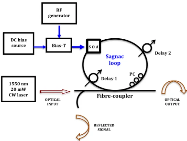
Fig. 2. Optical circuit diagram #2 of an interferometric optical modulator based on a Sagnac loop incorporating an electrically driven SOA.
The 1550 nmwavelength CW (unmodulated) light signal Pin = 20 mW power to be modulated is launched into the single
SOA or the Sagnac loop + SOA. In both circuits, the microwave carrier at fRF frequency and IRF current amplitude to
be transmitted along the optical fibre is launched into the SOA superimposed with a bias current Ibias by means a bias-T. The
composite signal is injected through the electrical port of the SOA. The SOA works as a one-travelling optical amplifier enhancing the energy of the switched light. In this way, the
launched optical signal is gain-modulated in the Circuit #1 and gain + phase-modulated in the Circuit #2 both by the Ibias + IRF
input. Because the SOA is asymmetrically inserted in the Sagnac loop (Fig. 2), a differential and periodic phase-shift Φ0senωt is modulated between the clockwise and
anti-clockwise interfering signals when IRF is launched, where ω =
2πfRF. Because of the long recovery-time of the SOA, the
negative cycle of the input microwave current is likely to be not clipped. The constant Φ0 depends on the nonlinearity
strength of the SOA, the recovery-time, the bias current and the asymmetry (38 ps/62 ps) of the inserted SOA into the Sagnac loop. By setting the Sagnac loop to operate in the linear region of the transfer function, the POUT (transmitted power) for small
phase-shift is given by (1) where the parameter B depends on losses and amplifier gain of PIN.
P!"#=1
2BP!" 1 − cos
π
2+ Φ!senωt
P!"#≈!!BP!" 1 + Φ!senωt (1)
The numerical simulations were first carried out using a single SOA in a travelling-wave configuration (non-interferometric) subject only to gain modulation. The second set of simulations was carried out using a SOA in an interferometric Sagnac based device subject to gain and phase modulation simultaneously. The SOA and electrical/optical supply parameters were the same for both configurations and none band-pass filter is used despite the setting of Ibias > 0 mA,
but limited to 50 mA.
III. RESULTS AND DISCUSSIONS A. Single SOA in travelling-wave configuration
Figure 3 shows three plots of the optical output from the
Circuit #1 at fRF = 20 GHz carrier frequency, IRF = 80 mA
microwave current amplitude, Ibias = 0, 10 and 50 mA bias
current, respectively. All plots are assigned with the optical offset level PDC and amplitude POUT of the output waveform.
Fig. 3. Outputs from the single SOA optical modulator at 20 GHz for 80 mA microwave current, biased with Ibias = 0, 10 and 50 mA.
When the SOA is unbiased, the output amplitude is very low (0.24 µW) with a high optical offset (129 µW). The origin
! RF generator DC bias source Bias-T 1550 nm 20 mW CW laser bulk 500 µm SOA OPTICAL INPUT OPTICAL OUTPUT ! ! ! ! ! ! ! ! ! ! ! Fibre&coupler, , Sagnac, loop, S,O,A, , ,, , Delay,2,, PC, , Delay,1,, RF, generator, , DC,bias, source, , Bias&T,! 1550,nm, 20,mW, CW,laser, , , OPTICAL, INPUT, , OPTICAL, OUTPUT, , REFLECTED, SIGNAL,
of the latter comes from the excitation of SOA with a high-frequency IRF microwave carrier that interacts with long-lived
charge carriers featuring recovery time > 1.4 ns, since 1.4 ns was previously characterised for Ibias = 100 mA (not shown
here).
When Ibias = 10 mA is applied, both offset PDC and output
amplitude POUT dramatically increases because much more
charge carriers are available in the conduction band. Therefore, the ratio POUT/PDC is increased from 0.24/124 =
0.002 to 0.43/1.3 = 0.331 (x 165.5 times). When Ibias = 50 mA
is applied, it leads to 4.2/15.9 = 0.264 comparable with the ratio achieved when Ibias = 10 mA. For all injected Ibias, the
SOA gain is not fully recovered because PDC > 0 mW.
B. Sagnac interferometer with a SOA inserted into the loop
Figure 4 shows four plots of the optical outputs from the
Circuit #2 by injecting drive signal of IRF = 80 mA amplitude
and fRF = 20 GHz microwave carrier frequency into the
unbiased (Ibias = 0 mA) SOA. Different output signals are
achieved by varying the polarisation bias (phase angle) of the Sagnac loop.
Fig. 4. Optical outputs from the Sagnac loop interferometer incorporating an unbiased (Ibias = 0 mA) SOA driven with 20 GHz frequency and 80 mA
microwave current amplitude. The polarisation bias of the loop are set at 0°, 26°, 50° and 90°.
As expected, for polarisation bias at 26° and 50° the output signals are distorted by clipping since the device operates in a non-linear region of the transfer curve. For 90° polarisation bias, a non-distorted signal very faithful with the input sinusoidal signal is calculated because the interferometer operates in the region of linear response with maximum derivative (quadrature). Nevertheless, for polarisation bias at 0°, the output waveform is little distorted because the interferometer operates in a maximum transmission around Φ0
= 0 rad (Ibias = 0 mA) since the light carrier is not suppressed
and the 2nd harmonic contribution is not very high. An
advantage by using 0° polarisation bias at Ibias = 0 mA for small
input signal (at least IRF < 80 mA), is to generate an output
optical signal accompanied with an almost null optical DC [17], but with a reduced amplitude when compared with the 90° (maximum linearity).
Figure 5 shows three plots of the optical output from the
Circuit #2 by injecting unbiased and biased (Ibias = 0, 10 and 50
mA) drive signal of IRF = 80 mA amplitude and fRF = 20 GHz
microwave carrier frequency. Different output signals are achieved by using the same polarisation bias of 90°. When the Ibias is increased, the PDC and the amplitude of optical output
signal POUT are also increased.
Fig. 5. Optical outputs from the Sagnac loop interferometer incorporating an unbiased (Ibias = 0 mA) and biased at Ibias = 10 and 50 mA SOA electrically
driven with 20 GHz frequency and 80 mA microwave current amplitude. The polarisation bias is set at 90° for all bias current.
When Ibias = 10 mA is applied, both PDC and POUT
dramatically increases because much more carriers are available. However, the ratio POUT/PDC is increased from
0.080/0.045 = 1.78 to 2.4/0.7 = 3.43 (x 1.93 times). When Ibias
= 50 mA is applied, it leads to 8.9/4.6 = 1.93, less than the ratio when Ibias = 10 mA. For all applied Ibias, the SOA gain is
not fully recovered. At least in the range 0-50 mA, the POUT
increases with Ibias, but not the POUT/PDC ratio.
C. General discussions
From ~ 300 MHz to 30 GHz even with unbiased SOA, none negative cycle clipping of the sinusoidal current input was already calculated for the optical output [17]. The clipping is expected since a SOA is a diode as LDs and LEDs are. A possible explanation is because the SOA presents a recovery-time greater than 1.4 ns when it is biased with Ibias < 50 mA.
Therefore, for fRF > 300 MHz the period of the input signal
becomes lesser than the recovery-time, e.g. 1/20 GHz = 50 ps is at least ~ 28 times less. The “memory effect” of SOAs seems to be useful for continuous analogue signals whereas the resulting pattern effect is likely to appear for digital streams [18]. When the SOA is biased, carriers are injected in the conduction band by the Ibias and the contribution of IRF is less
critical. However, the devices become noisier due the ASE generation. SOAs biased below the transparency current should be further investigated since it is still almost noiseless.
It was already reported [17] for low microwave current amplitude (IRF = 1 mA and fRF = 5 GHz) a flat response from
0.3 to 10 GHz and fCUT = 26 GHz cut-off frequency for the
interferometric device whereas the single SOA was not able to respond in either input frequency.
Now, from the calculated plots shown in Figs. 3 and 5, the Table I show the comparison between the POUT and PDC from
the single SOA and Sagnac with an inserted SOA (polarisation bias = 90°) modulators electrically driven by IRF = 80 mA and
fRF = 20 GHz.
Table I shows that when both devices are unbiased a dramatic increase around x188 times is observed for the POUT
whereas a modest decrease of PDC is calculated when the SOA
is inserted into a Sagnac loop. When the devices are biased, both POUT and PDC increase as Ibias is augmented. However, the
increase of POUT is less dramatic when Ibias > 0 mA and is
increased when the SOA is again inserted into the Sagnac loop. Moreover, it is achieved a greater decrease of PDC.
TABLE I. COMPARISON OF OUTPUT POWERS FROM SINGLE SOA AND
SAGNAC INTERFEROMETER +SOAMODULATORS
Ibias (mA) Power SOA Sagnac with
SOA Increase (dB) 0 POUT 0.24 µW 45 µW + 22.7 PDC 129 µW 80 µW - 2.1 10 POUT 0.43 mW 2.4 mW + 7.5 PDC 1.3 mW 0.7 mW - 2.7 50 POUT 4.2 mW 8.9 mW + 3.3 PDC 15.9 mW 4.6 mW - 5.4
As a result of present simulations and those shown on [17] for small microwave current amplitude, a significant improvement of performance is achieved when the electrically driven SOA is merely inserted into a Sagnac loop despite the long recovery-time of the amplifier when compared with the period of the microwave carrier to be modulated.
As modulation frequency increases, traveling-wave effects can degrade the bandwidth of directly modulated laser diodes (LDs) [19]. Furthermore, pulses are generated with optical chirp that in general negatively interacts with the fibre chromatic dispersion thus limiting the bandwidth. In order to circumvent the limitations of directly modulated light sources, some devices have being used and are firmly established as external optical modulators as Mach-Zehnder electro-optic (MZ-EOM) and electro-absorption (EAM) modulators in analogue [20] and digital modulations.
In principle, the SOA itself exhibits a reduced intrinsic capacitance because of its low length typically of 0.5 mm whereas a typical MZ-EOM presents electrode length in the few mm to few tenths mm range [21]. However, the package parasitics of SOAs should not be neglected [22]. By using an unpackaged device [23] the parasitics of SOA may be reduced and fRF > 10 GHz electrical modulation was already achieved.
It has been shown that at microwave frequencies, typically above 10 GHz, usually the electrode geometry of SOAs yields a large propagation loss, which means that the details of the way the modulation signals are fed to the device becomes important [4].
A more detailed comparative analysis still needs to be carried out amongst the MZ-EOMs, EAMs and SOAs-based modulators. However, SOAs can automatically amplify the signals, has a very high and fast nonlinearity (e.g. quantum-dot SOAs), when inserted in an interferometric device it can perform several functions simultaneously and due it reduced size the resulting circuit is prone to optical integration.
IV. CONCLUSIONS
In this work, were reported two electrically driven SOA-based devices able to receive a guided or free-propagating microwave carrier thus creating a sub-carrier onto the light wave.
The first device is the well-known single SOA operating in travelling-wave regime where the microwave carrier modulates the gain of the amplifier. In the second device, the same SOA is merely inserted into an interferometric Sagnac loop where the microwave carrier simultaneously modulates the gain of the amplifier and the differential phase between the counter-propagating signals. As a result, the modulation efficiency was significantly improved for very low microwave current amplitude (< 1 mA) at 5 GHz when the device is used as a probe [17] and for electrically amplified input (80 mA) at 20 GHz.
Even though the adopted SOA model presents a long recovery-time > 1.4 ns, both configuration and mainly the interferometric one, could be modulated at 20 GHz carrier frequency and higher.
The main aims of this paper were to show the improvements when an interferometric configuration is used instead of a single SOA and to take the advantage of the partial recovery gain for high-frequency modulation. In practice, it is not easy to directly modulate a SOA in carrier frequencies higher than 10 GHz [22,23], but improvements have being achieved.
Further numerical simulations regarding device sensitivity under variations of many physical parameters and also including the electrical model of SOA/package are on going. Experimental validations are also scheduled to be held in our laboratory.
ACKNOWLEDGMENT
Ricardo M. Ribeiro thanks the team at Département d’Optique of Telecom Bretagne and the CapilRTM platform for
hosting his Post-Doctoral study during which the present work was carried out. The authors also thank Cristina Arellano of VPI Photonics GmbH for her technical help.
REFERENCES
[1] H. Al-Raweshidy and S. Komaki, editors, Radio over Fiber Technologies for Mobile Communications Networks, Artech House, 2002.
[2] S.R. Abdollahi, H.S. Al-Raweshidy and R. Nilavalan, “Fully-Photonic Analogue-to-Digital Conversion Technique for Super-Broadband Digitized-Radio over Fibre Link”, 16th European Conference on
Networks and Optical Communications, Newcastle, UK, July 20-22, pp. 72-75, 2011.
[3] R.C. Williamson and R.D. Esman, “RF Photonics”, Journal of Lightwave Technology, vol. 26, no. 9, pp. 1145-1151, 2008.
[4] J. Mork, A. Mecozzi and G. Eisenstein, “The Modulation Response of a Semiconductor Laser Amplifier”, J. of Selected Topics in Quant. Elect., vol. 5, no. 3, pp. 851-860, 1999.
[5] A. Nirmalathas, P.A. Gamage, C. Lim, D. Novak and R. Waterhouse, “Digitized Radio-Over-Fiber Technologies for Converged Optical Wireless Access Network”, Journal of Lightwave Technology, vol. 28, no. 16, pp. 2366-2375, 2010.
[6] A. Saadani et al, “Digital Radio over Fiber for LTE-Advanced: Opportunities and Challenges”, 17th Conference on Optical Network
Design & Modeling (ONDM 2013), Brest, France, April 16-19, pp. 193- 198, 2013.
[7] R.M. Ribeiro, F. Lucarz and B. Fracasso, “A Thresholder for All-Optical Digitising Radio-over-Fibre Transceivers”, 17th Conference on Optical
Network Design & Modeling (ONDM 2013), Brest, France, April 16-19, pp. 160-165, 2013.
[8] R.M. Ribeiro, F. Lucarz and B. Fracasso, “An All-Optical Sampler for Digitising Radio-over-Fibre Transceivers”, 8th IEEE Conference on
Network and Optical Communications (NOC 2013), July 10-12, Graz, Austria, pp. 27-34, 2013.
[9] R.M. Ribeiro, F. Lucarz and B. Fracasso, “Proposal and Design of an All-Optical Encoder for Digitising Radio-over-Fibre Transceivers”, 18th
European Conference on Network & Optical Communications (NOC 2013), Graz, Austria, July 10-12, pp. 35-42, 2013.
[10] R.M. Ribeiro et al, “An Optical Pulse Generator from a Sinusoidal Optical Signal Using Sagnac Loop – Self-Sampling”, 5th IEEE
Latin-American Conference on Communications (LATINCOM 2013), Santiago, Chile, November 24-26, 2013.
[11] R.M. Ribeiro, V.N.H. Silva, A.P.L. Barbero, F. Lucarz and B. Fracasso, “Design of an Analogiser for Optically Digitised Radio-over-Fibre Signals”, accepted in the ICTON 2014, unpublished.
[12] F.X. Kärtner et al, “Electronic Photonic Integrated Circuits for High Speed, High Resolution, Analog to Digital Conversion”, Proceedings of SPIE, vol. 6125, 612503, 2006.
[13] T. Rampone et al, “ Conversion gain characterisation of optical radiofrequency signal mixing by all-optical sampling on SOA-MZI”, Electronics Letters, vol. 48, no. 24, pp. 1542-1543, 2012.
[14] J. Capamany, S. Sales, D. Pastor and B. Ortega, “Optical mixing of microwave signals in a nonlinear semiconductor laser amplifier modulator”, Optics Express, vol. 10, no. 3, pp. 183-189, 2002.
[15] M. Eiselt, “Optical Loop Mirror with Semiconductor Laser Amplifier”, Electronics Letters, vol. 28, no. 16, pp. 1505-1507, 1992.
[16] M. van der Poel, D. Birkedal, J. Hvam, M. Laemmlin and D. Bimberg, “Alpha parameter in quantum-dot amplifier under optical and electrical carrier modulation”, CLEO 2004, San Francisco, USA, May 16-21, 2004.
[17] R.M. Ribeiro, V.N.H. Silva, A.P.L. Barbero, F. Lucarz and B. Fracasso, “Sagnac Loop Incorporating a Semiconductor Optical Amplifier Without Bias Current to Receive/Modulate Weak RF Signals”, accepted in the ICTON 2014, unpublished.
[18] K.E. Zoiros, T. Siarkos and C.S. Koukourlis, “Theoretical analysis of pattern effect suppression in semiconductor optical amplifier utilizing optical delay interferometer”, Optics Comm., vol. 281, pp. 3648-3657, 2008.
[19] S. Iezekiel, “Travelling-Wave Effect in Microwave Photonics”, IEEE LEOs Annual Meeting Conf. Proceedings LEOS’09, October, 4-8, pp. 658-659, 2009.
[20] C.H. Cox III, “Analog Optical Links: Theory and Practice, Cambridge University Press, 2004.
[21] Ed L. Wooten et al, “A Review of Lithium Niobate Modulators for Fiber-Optic Communications Systems”, IEEE J. of Selec. Top. in Quant. Elect., vol. 6, no. 1, pp. 69-82, 2000.
[22] A.L. Toazza, M. Guimarães, C.A.C. Petersen, C.M. Gallep and E. Conforti, “Experimental and Theoretical Analysis of Packaging Inductances and Stray Capacitances of a Semiconductor Optical Amplifier”, 2006 International Telecommunication Symposium (ITS 2006), Fortaleza, CE, Brasil, September 3-6, pp. 63-66, 2006.
[23] R.C. Figueiredo, N.S. Ribeiro, E. Conforti and C.M. Gallep, “Chip-on-Carrier Microwave Mount for Semiconductor Optical Amplifier Measurement”, IMOC 2013, August 4-7, Rio de Janeiro, Brasil, 2013.