HAL Id: hal-02270910
https://hal.archives-ouvertes.fr/hal-02270910
Submitted on 26 Aug 2019
HAL is a multi-disciplinary open access
archive for the deposit and dissemination of
sci-entific research documents, whether they are
pub-lished or not. The documents may come from
teaching and research institutions in France or
abroad, or from public or private research centers.
L’archive ouverte pluridisciplinaire HAL, est
destinée au dépôt et à la diffusion de documents
scientifiques de niveau recherche, publiés ou non,
émanant des établissements d’enseignement et de
recherche français ou étrangers, des laboratoires
publics ou privés.
Generation of O-band PAM-4 signal using a silicon
modulator driven by two binary sequences
Lucas Deniel, Mathilde Gay, Diego Perez-Galacho, Charles Baudot, Laurent
Bramerie, Oskars Ozolins, Frédéric Boeuf, Laurent Vivien, Christophe
Peucheret, Delphine Marris-Morini
To cite this version:
Lucas Deniel, Mathilde Gay, Diego Perez-Galacho, Charles Baudot, Laurent Bramerie, et al..
Gen-eration of O-band PAM-4 signal using a silicon modulator driven by two binary sequences. SPIE
Photonics West - OPTO 2019, Feb 2019, San Francisco, France. pp.40. �hal-02270910�
Generation of O-band PAM-4 signals using a silicon modulator driven
by two binary sequences
L. Deniel*
a, M. Gay
b, D. Pérez-Galacho
a, C. Baudot
c, L. Bramerie
b, O. Ozolins
d, F. Boeuf
c, L.
Vivien
a, C. Peucheret
b, D. Marris-Morini
aa
Centre de Nanosciences et de Nanotechnologies, CNRS, Univ. Paris-sud, Université Paris-Saclay,
91120 Palaiseau, France;
bUniv Rennes, CNRS, FOTON – UMR 6082, F-22305 Lannion, France;
c
ST Microelectronics, 850 rue Jean Monnet, 38920 Crolles, France;
dNetworking and transmission
Laboratory, RISE AB, Kista, Sweden
ABSTRACT
Silicon photonics is a promising solution for next generation of short-range optical communication systems. Silicon modulators have driven an important research activity over the past years, and many transmission links using on-off keying modulation format (OOK) were successfully demonstrated with a large diversity of modulator structures. In order to keep up with the demand of increasing bitrates for limited bandwidths in Datacom applications, higher modulation formats are explored, such as quadrature phase shift keying (QPSK) or 4-level pulse amplitude modulation (PAM-4). However, driving the modulators to generate PAM-4 signals commonly require expensive and power-hungry electronic devices such as digital-to-analog converters (DACs) for pulse-shaping and digital signal processors (DSP) for non-linearity compensation. Lastly, new solutions were studied to overcome this issue, including new driving methods based on the use of two different input binary sequences applied directly on the modulator. While most of the reported works are focused on the C-band of communication, the O-band can present a definitive advantage due to the low dispersion of standard single-mode (SSMF) fiber. For those reasons, we demonstrate the generation of a 10-Gbaud DAC-less PAM-4 signal in the O-band using a depletion-based silicon traveling wave Mach-Zehnder modulator (TWMZM). An open eye diagram was obtained, and a bit error rate (BER) of 3.810-3 was measured for a received optical power of about -6 dBm.
Keywords: PAM-4, silicon photonics, modulator, Mach Zehnder modulator, O-band
1. INTRODUCTION
On-off keying (OOK) modulation format may no longer keep up with the increasing spectral efficiency requirements for 400Gb/s intensity modulation / direct detection (IM-DD) intra-datacenter short-reach transmissions. Therefore, 4-level pulse amplitude modulation (PAM-4) format is considered as an interesting choice for this standard [1]. Among the different modulator technologies, silicon photonics present the benefit of allowing small footprints, high flexibility, low energy consumption, compatibility with the complementary metal oxide semiconductor (CMOS) fabrication process, and possibility of integration with electronics.
For these reasons many silicon modulator structures based on free-carrier plasma dispersion effect have been studied and compared over the past few years [2]. Modulators are key elements to reduce the power consumption of a transmission link, but with PAM-4 modulation, the electrical driving scheme contains itself power hungry devices such as digital to analog converters (DACs), which are used to convert 2-level non-return-to-zero (NRZ) sequences into 4-level ones. Several dual-embedded structures based on ring modulators (RM), Mach Zehnder modulators (MZM) or segmented electrodes modulators have been investigated to optically generate a 4-level signal relieving the need for an electrical DAC [3-5]. They rely on the principle that it is possible to drive each of the two structure parts directly with a different NRZ electrical signal and combining these signals in the optical domain to obtain 4 distinct intensity levels. Most of the demonstrations were performed in the C-band. Among all of these structures, L. Zheng et al. showed that it is possible to use a dual-drive MZM to obtain PAM-4 levels out of two binary electrical signals of different peak-to-peak voltages, by applying each signal on a different arm of the MZM [6]. Interestingly, this simple and generic dual-drive MZM is one of the most flexible as it not only allows to generate intensity modulation formats but also phase modulation formats, simply by driving it in a proper way [7]. However, it is not straightforward to find out the peak-to-peak voltage values to apply on each arm of the modulator in order to reach 4 equally spaced levels while benefiting from the full dynamic
range. We thus developed and used a model for this purpose. After introducing the MZM design and characterization (static and dynamic), we focus on PAM-4 generation. We compare the model we developed for PAM-4 generation, based on realistic the phase shifter performances, i.e. effective index and absorption coefficient variations in the phase shifters with respect to the applied voltages, to a simple ideal and lossless MZM model. Then, we demonstrate 20Gb/s PAM-4 generation using the silicon MZM. This work is the first report of PAM-4 generation in the O-band based on a simple dual-drive silicon MZM.
2. MODULATOR DESIGN AND CHARACTERIZATION.
2.1 Device design
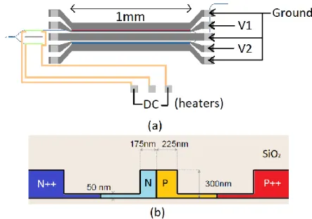
Figure 1. (a) Schematic top view of the dual-drive MZM, each phase shifter can be driven independently through coplanar travelling-wave electrodes, and thermal heaters controlled with a DC voltage can be used to tune the operating point. (b) Schematic cross section of one phase shifter, the carrier depletion regime in the PN junction is used to achieve phase modulation along the rib waveguide.
A schematic top view of the MZM structure can be seen in Fig. 1(a). A 3 dB 1×2 multimode interference (MMI) coupler splits the light from an input waveguide into two arms of same lengths containing phase shifters, and another 3 dB 1×2 MMI coupler combines the light from both arms into the output waveguide. Grating couplers are used for fiber-to-chip transitions. The cross-section of a phase shifter is shown on Fig. 1(b). The phase shifter is 1mm long, the waveguide height is 300 nm and its width is 400 nm while the rib part thickness is 50 nm. As the modulator is designed to operate in the depletion regime, a PN junction is realized, the P region is doped with a 5×1017 cm-3 targeted Bore concentration and
the N region is doped with a 4.5×1017cm-3 targeted Phosphorus concentration. It can be seen that the junction between P
and N regions is shifted by 25nm apart from the waveguide center towards the N-doped region, improving the overlap between the P-doped area and the optical TE fundamental mode-profile, which leads to a more efficient phase shifter. Higher P++ and N++ doping concentrations of 1019 cm-3 are used close to the electrical contacts to reduce the access
resistance of the phase shifters, increasing the modulator bandwidth. The coplanar-waveguide (CPW) electrodes are ended with pads which allow them to be accessed with GSGSG probes. On each arm, metallic strips close to a passive part of the waveguides are used as resistors (heaters) to thermally tune the operating point of the MZM under the application of a DC voltage. The MZM was fabricated at ST-Microelectronics on a 300 mm SOI technological platform [8].
2.2 Static characterization and loss modeling
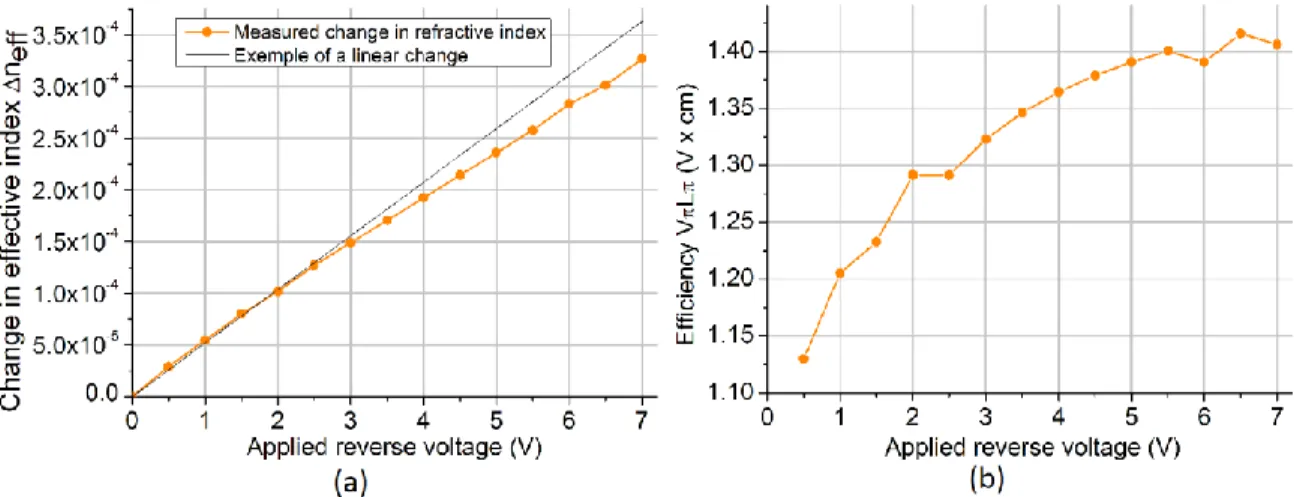
To measure the phase shifter efficiency, ring resonators have been fabricated on the same photonic circuits. Indeed, by tracking the resonant wavelength shifts with the applied voltage, it is possible to deduce the effective index variation of the optical mode. An 80-µm radius ring resonator is used to this end. The PN junction is embedded in the ring, covering 87% of its perimeter. By measuring the resonance wavelength shift of the resonator for different applied DC voltage on the phase shifter, it is possible to calculate the corresponding change in effective refractive index of the optical mode and thus the efficiency (V×L product) of the phase shifter as a function of the applied reverse voltage. A 3.3×10⁻⁴ change in
effective index is measured between 0 V and 7 V (Fig. 2), corresponding to an efficiency of 1.13 V×cm around 0.5 V and 1.41 V×cm around 7V.
Figure 2. (a) Experimental change in the effective refractive index of the mode as a function of the DC applied reverse voltage on the phase shifter. (b) Corresponding change in the VL efficiency product as a function of the DC applied reverse voltage on the phase shifter.
Free carrier concentration variations are responsible for effective index variations but also absorption coefficient variations. A numerical model is used to evaluate the optical mode propagation losses. The free carrier concentrations within the phase shifter are given by a 1D electrical stimulation as a function of the applied reverse voltage. Absorption coefficients are then calculated from these carrier concentrations using Soref equations. Finally, a mode solver allows to estimate the resulting effective attenuation factor of the waveguide. From Fig. 3, we can see that these losses are estimated to be 1.8 dB×mm-1 at 0V and 1.14 dB×mm-1 at 7 V.
Figure 3. Optical losses in the phase shifter as a function of the DC applied reverse voltage, according to a simulation based on free carrier concentration variations.
2.3 Bandwidth characterization
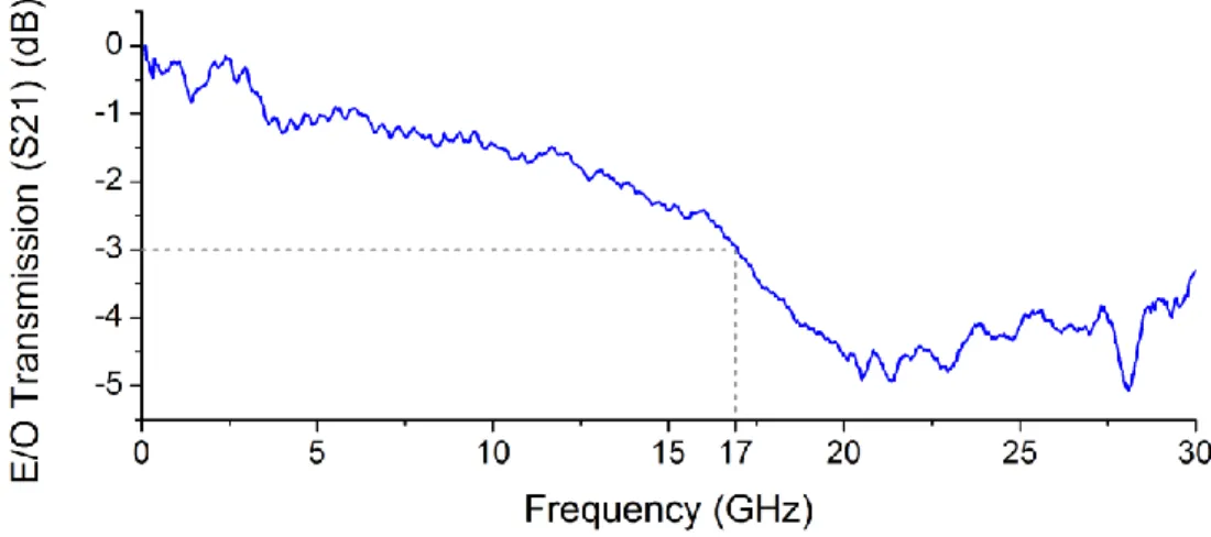
An electro-optical bandwidth measurement is performed using Agilent 86030A 50GHz Lightwave Component Analyzer. For this measurement, the PN junction is biased under -4 V, and a 50 Ω termination is loaded at the end the RF line to avoid reflections. The normalized spectrum (Fig. 4) shows a 17 GHz bandwidth.
Figure 4. Normalized Electro-Optical transmission spectrum of the MZM (S21), the measured bandwidth is 17 GHz (3dB-bandwidth in the optical domain).
3. PAM-4 MODEL
When two binary electrical signals with different amplitudes are applied on both arms of the MZM, 4 levels of transmissions can be reached, as described in [6]. To obtain the lowest bit error rate, the levels should be equally spaced, and the extinction ratio must be maximized to work with the best signal-to-noise ratio. This section will introduce and compare two different models for finding out which peak-to-peak voltages to apply on each arm in order to respect the two aforementioned conditions. The first model is based on a simplified ideal MZM, while the second one is more realistic and takes account of the phase shifters behavior described in section 2.2. Finally, these models are compared to each-other.
3.1 Simplified model of an ideal dual-drive MZM
In the ideal case of a linear variation of the effective index with the voltage, and loss-less phase shifters, the transfer function of a MZM can be expressed as:
1 1 cos 2 OUT H IN I V I V = + + (1)
Where IOUT is the output optical intensity, IIN is the input optical intensity, V is the difference between the voltages
applied on the two phase shifters, V is the voltage required on one phase shifter to obtain a phase difference between the electric fields at the end of each arm, and H is the static phase difference set by tuning the DC voltage applied on
heaters. The voltage differences between the two phase shifters in order to get specific transmission levels can then be found by reversing the above equation and solving it for each desired transmission levels. In the case of 4 equally spaced levels with a maximum transmission of 1 and a minimum of 0, the peak-to-peak voltages to apply on the first arm (VPP1)
and on the second arm (VPP2) of a quadrature-biased MZM can be expressed in a simple way:
1 2 1 1 arcsin 2 3 PP V V = − (2)
2 1
PP PP
V =V −V (3)
According to Fig 2, the mean V L is 1.36 V. Considering a static phase imbalance of H=/2, assuming the phase
shifters lengths are 1mm and that they are both biased at -4 V, the optimized peak-to-peak voltages given by this ideal MZM model are VPP1 = 8.3 V and VPP2 = 5.34 V.
3.2 Realistic model of the silicon dual-drive MZM
It was shown in section 2 that for the silicon MZM, the effective index variation in the phase shifters are not linear with the applied voltage, and their loss depends on the applied voltage. Therefore, the output electric field must be written as:
2 2 1 2 2 H H j j OUT E e E e E − + = (4)
with En being the electric field at the output of phase shifter n, such that:
(
)
(
)
(
)
IN exp ( ) exp j2 ( )
2
n eff eff n eff eff n
E E V L n n V L = − + + (5)
Where EIN is the electric field at the input of the MZM, L the length of the phase shifter, Vn the voltage applied on the
phase shifter n, the laser wavelength, eff the effective attenuation factor of the phase shifters, eff the effective
attenuation variation introduced by the application of the voltage Vn on the phase shifter n, neff the effective index of the
phase shifters, neff the effective index variation introduced by the application of the voltage Vn on the phase shifter n.
Equation 4 and 5 can be used to determine numerically the optimized peak-to-peak voltages to apply on each phase shifter in order to reach 4 equally-spaced levels while benefiting from the full dynamic range of the transfer function. The static characteristics reported in section 2.2 are used (effective index variation and absorption coefficient as a function of the applied voltage). From the calculation the following optimized peak-to-peak voltages are obtained:
VPP1 = 8 V and VPP1 = 4.72 V.
3.3 Model comparison
Fig. 5 shows the obtained transmission levels on the silicon MZM model, by applying peak-to-peak voltages given by (a) the ideal MZM model, and (b) the silicon MZM model. The black curves represent the push-pull transmission of the MZM (opposite voltages are applied on the arms), and the red lines represent the reached PAM-4 levels for given peak-to-peak voltages VPP1 and VPP2. As it can be seen from this figure, neglecting the losses and non-linearities of the phase
shifters gives rise to inequalities between levels spacing: with the voltages given by the simplified ideal model, the middle level is only 29.5% of the full dynamic range, while both external spacings are 35%. With the realistic model voltages, all the spacings are close to 33.3%.
Figure 5. PAM-4 transmission levels resulting from the application on the realistic silicon MZM model of peak-to-peak voltages given by (a) the ideal lossless MZM model (8.3V on one arm and 5.34V on the other) and (b) the realistic silicon MZM model (8V on one arm and 4.72V on the other).
4. PAM-4 BER MEASUREMENTS
The experimental setup consists in two parts. For the optical part, an O-band external cavity laser emits light at 1.31µm wavelength, the beam is then amplified through a semiconductor optical amplifier (SOA) before being coupled in and out of the chip (coupling losses are about 5dB per grating coupler). At the receiver side, light is amplified with a praseodymium amplifier and split by a 3 dB directional coupler, one half of the power feeds a 40GHz photodiode followed by a 35GHz travelling wave amplifier and the resulting signal is sent to the error counter of a BER tester, while the other half is sent to a 25 GHz real time oscilloscope displaying the eye diagram in real time. For the electrical part, two complementary 10 Gb/s 215-1 pseudo-random binary sequences are first generated, one of them is delayed by 200 ps
thanks to an RF delay line. Both signals are then amplified by means of tunable gain RF amplifiers and a 4 V reverse DC voltage is added on each line with bias tees to bias the PN-junction. At the output, both lines are terminated with 50 Ω loads after DC blocks. The gain of the RF amplifiers is used to tune independently the peak-to-peak voltages applied on each arm of the MZM.
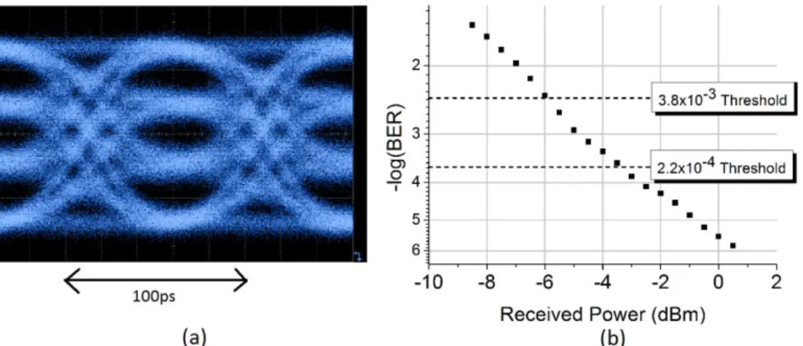
For this experiment, the power received on the photodiode is swept from -8.5 dBm to 0.5 dBm. The peak-to-peak voltages are set to 7 V on the first arm and 4V on the second one to almost use the full dynamic range and obtain equally-spaced levels. The resulting BER curve is plotted in Fig. 6.
Figure 6. (a) 20 Gb/s PAM-4 opened eye diagram at 0 dBm received power. (b) 20Gb/s PAM-4 BER against received power. The silicon MZM is driven with VPP1=7V and VPP2=4V in both figures.
It can be seen from Fig. 6(b) that the link BER is under the hard-decision forward error correction (HD-FEC) threshold of 3.8×10⁻³ for a received power of -6dBm, under the KP4-FEC threshold of 2.2×10⁻⁴ for a received power of -3.4dBm
and reaches a value as low as 1.54×10⁻⁶ for a received power of 0.5dBm. The transitions in the eye diagram (Fig. 6(a))
suggests that these results could be further improved by increasing the MZM bandwidth.
5. CONCLUSION
To fulfill the increasing spectral efficiency requirements in intra-datacenter data-communications, IM-DD PAM-4 modulation format is considered as an interesting choice, and silicon photonics is a well-suited technology. It is possible to use a simple and flexible silicon MZM structure to optically generate four intensity levels out of two binary NRZ electrical signals with different amplitudes, removing the need for power hungry DACs within the electrical driving systems. However, this PAM-4 generation method requires conveniently tuned driving voltage amplitudes.
After introducing an O-band silicon MZM, a realistic model for the MZM transmission was presented, taking account of the phase shifters static properties. This model was compared to a simpler one based on an ideal lossless MZM and a significant difference was highlighted between the two. At last, a demonstration of a 20Gb/s O-band PAM-4 transmission was performed, with a measured BER under the HD-FEC threshold of 3.8×10⁻³ for a received power of
-6dBm and reaching a value as low as 1.54×10⁻⁶ for a received power of 0.5dBm.
ACKNOWLEDGMENT
This work was supported by the European project Cosmicc (H2020-ICT-27-2015-688516).
REFERENCES
[1] IEEE P802.3bs 400 GbE Task Force. http://www.ieee802.org/3/bs/index.html (6 December 2017)
[2] Shi, W., Xu, Y., Sepehrian H., LaRochelle, S. and Rusch, L. A., “Silicon photonic modulators for PAM transmissions,” J. Opt. 20(2), 083002 (2018).
[3] Moazeni, S., Lin, S., Wade, M., Alloatti, L., Ram, R. J., Popović, M. and Stovanović, V., “A 40-Gb/s PAM-4 transmitter based on a ring-resonator optical DAC in 45-nm SOI CMOS,” IEEE J. of Solid State Circuit 52(12), 3503-3516 (2017).
[4] Samani, A., Veerasubramanian, V., El-Fiky, E., Patel, D. and Plant, D., “A silicon photonic PAM-4 modulator based on dual-parallel Mach-Zehnder interferometers,” IEEE Photon. J. 8(1), 1-10 (2016).
[5] Dubray, O., Seyedi, M. A., Chen, C. H., Charbonnier, B., Descos, A., Fiorentino, M., Beausoleil, R. G. and Menezo, S., “30Gbit/s PAM-4 transmission by modulating a dual silicon ring resonator modulator,” Proc. IEEE Optical Interconnects Conference, 6-7, (2016).
[6] Zheng, L., Ding, J., Shao, S., Zhang, L. and Yang, L., “Silicon PAM-4 optical modulator driven by two binary electrical signals with different peak-to-peak voltages,” Opt. Lett. 42(11), 2213-2216 (2017).
[7] Perez-Galacho, D., Bramerie, L., Baudot, C., Chaibi, M., Messaoudène, S., Vulliet, N., Vivien, L., Bœuf, F., Peucheret, C. and Marris-Morini, D., “QPSK modulation in the O-band using a single dual-drive Mach-Zehnder silicon modulator,” J. Lightw. Technol. 36(18), 3935-3940 (2018).
[8] Baudot, C., Fincato, A., Flower, D., Perez-Galacho, D., Souhaité, A., Messaoudène, S., Blanc, R., Richard, C., Planchot, J., De-Buttet, C., Orlando, B., Gays, F., Mezzomo, C., Bernard, E., Marris-Morini, D., Vivien, L., Kopp C. and Boeuf F., “Daphne silicon photonics technological platform for research and development on WDM applications,” Proc. SPIE 9891, 98911D (2016).