Embedded Vector Measurement of RF/Microwave Circuits in
LTCC Technology
by
Hana MOHAMED
THESIS PRESENTED TO ÉCOLE DE TECHNOLOGIE SUPÉRIEURE
IN PARTIAL FULFILLMENT FOR A MASTER’S DEGREE
WITH THESIS IN ELECTRICAL ENGINEERING
M.A.Sc.
MONTREAL, MAY 8, 2019
ÉCOLE DE TECHNOLOGIE SUPÉRIEURE
UNIVERSITÉ DU QUÉBEC
This Creative Commons licence allows readers to download this work and share it with others as long as the author is credited. The content of this work can’t be modified in any way or used commercially.
BOARD OF EXAMINERS
THIS THESIS HAS BEEN EVALUATED BY THE FOLLOWING BOARD OF EXAMINERS
Mr. Ammar B. Kouki, Thesis Supervisor
Department of Electrical Engineering at École de technologiesupérieure
Mr. NaimBatani, President of the Board of Examiners
Department of Electrical Engineering at École de technologiesupérieure
Mr. Francois Gagnon, Member of the Board of Examiners
Department of Electrical Engineering at École de technologiesupérieure
THIS THESIS WAS PRENSENTED AND DEFENDED
IN THE PRESENCE OF A BOARD OF EXAMINERS AND PUBLIC 18 OF APRIL 2019
ACKNOWLEDGMENT
I would like to take this opportunity to thank all the students and the members of LACIME laboratory for their generous support during this research project.
First of all, I would like to express my gratitude to my ebullient supervisor, Prof. Ammar B. Kouki for his wonderful support, encouragement, and advices to complete the research project successfully. I would also like to thank Mr. Normand Gravel for his patience and assistance in fabricating the many prototypes of my designs. Further, I am also thankful to my colleagues in ÉTS for their constant support and assistance during the research work.
I also appreciate the Ministry of Education of Libya for their financial support of my own studies and that of the entire Libyan student community who are pursuing Masters and PhD studies in Canada. I am also thankful to my family in Libya: my father, mother, and brother who advised and encouraged me to pursue graduate studies in Canada. Finally, I am humbled by the patience and support provided by my husband, daughter and son during my studies. I dedicate this project to my country Libya, my family, and my friends.
I am glad to work and study in ÉTS where scientific research goes parallel with latest industrial technology. The international atmosphere at ÉTS helped me to showcase my technical expertise and enhanced my knowledge.
Mesure vectorielle intégrée de circuits RF / micro-ondes dans la technologie LTCC Hana MOHAMED
RESUME
Alors que le nombre de systèmes et de normes sans fil continuent à augmenter, la réutilisation de matériel RF devient de plus en plus importante pour réduire les coûts et la taille et éliminer la redondance inutile des composants. Un moyen de maximiser la réutilisation du matériel RF consiste à déployer des circuits reconfigurables. Cela dépend à son tour de la mesure vectorielle intégrée pour garantir le bon fonctionnement du matériel reconfigurable.
Les techniques classiques de mesure vectorielle nécessitent des analyseurs de réseau vectoriel coûteux et encombrants ou des jonctions six ports légèrement plus compactes. Les deux options nécessitent l’utilisation de coupleurs directionnels pour l’échantillonnage des ondes progressives, ce qui augmente leur taille et limite leur aptitude à l’intégration dans du matériel RF reconfigurable. Les interféromètres à quatre ports non directionnels offrent une solution alternative pour la mesure vectorielle intégrée, caractérisée par une très petite taille, un très faible couplage et une facilité d'intégration.
Dans le présent travail, un nouveau réflectomètre 3D non directionnel à 4 ports pour la mesure de coefficients de réflexion complexes est proposé. Le réflectomètre proposé comporte deux renifleurs non directionnels optimisés placés sous une ligne de transmission avec des lignes enterrées pour acheminer les signaux reniflés aux détecteurs de puissance de la technologie LTCC. Les transitions verticales des lignes enterrées à la surface sont conçues et optimisées. Des simulations de champs électromagnétiques en 3D permettent d'optimiser la conception proposée afin d'obtenir le paramètre S de la structure. Deux circuits de détection de puissance LT5582 avec une plage dynamique de 57 dB sont utilisés pour détecter la puissance couplée. Un prototype du réflectomètre proposé est fabriqué au LTCC (Ferro L8) dans le laboratoire LACIME et utilisé pour mesurer 45 charges complexes différentes. Les résultats obtenus montrent un excellent accord avec les mesures VNA montrant des erreurs inférieures à 0,3 dB pour l'amplitude et inférieures à 3 ° pour la phase.
Embedded Vector Measurement of RF/Microwave Circuits in LTCC Technology Hana MOHAMED
ABSTRACT
As the number of wireless systems and standards continues to increase, RF hardware re-use is becoming more and more important to reduce cost and size and eliminate unnecessary component redundancy. One way of maximizing RF hardware re-use is to deploy reconfigurable circuits. This is turn relies on embedded vector measurement to ensure the reconfigurable hardware operates as required.
Conventional vector measurement techniques require costly and bulky Vector network analyzers or slightly more compact six-port junctions. Both options require the use directional couplers to sample forward and backward traveling waves, which increases their size and limits their suitability for embedding in reconfigurable RF hardware. Non-directional four-port interferometersoffer an alternative solution for embedded vector measurement that is characterized bya very small size, very low coupling, and ease of integration.
In the present work, a new 3D 4-port non-directional reflectometer for measuring complex reflection coefficients is proposed. The proposed reflectometer features two optimized non-directional sniffers positioned below a transmission line with buried lines to carry the sniffed signals to power detectors in LTCC technology. Vertical transitions from the buried lines to surface are designed and optimized. 3D electromagnetic field simulations are used to optimize the proposed design in order to obtain the S-parameter of the structure. Two LT5582 power detector circuits with 57 dB dynamic range are used to detect the coupled power. A prototype of the proposed reflectometer is fabricated in LTCC (Ferro L8) in LACIME laboratory and used to measure 45 different complex loads. The obtained results show excellent agreement with VNA measurements showing errors below 0.3 dB for amplitude and below 3° for phase.
TABLE OF CONTENTS
Page
INTRODUCTION ...1
CHAPTER 1 VECTOR MEASUREMENT TECHNIQUES ...7
1.1 Introduction ...7
1.2 Architectures of Network Analyzers ...8
1.2.1 Scalar Network Analyzers ... 8
1.2.2 Vector Network Analyzers ... 10
1.3 Six-Port Techniques ...13
1.3.1 Overview ... 13
1.3.2 The Six-Port Reflectometer ... 17
1.4 Phase and Gain Detection ...21
1.5 Conclusion ...22
CHAPTER 2 PROPOSED REFLECTOMETER ...23
2.1 Related Work ...23
2.2 Proposed 3D Four-Port Reflectometer Description ...24
2.3 Reflection Coefficient Determination ...26
CHAPTER 3 PROPOSED REFLECTOMETER ...31
3.1 Microstripline Design and Simulation ...32
3.2 Sniffer Design ...34
3.3 Perpendicular Transition Design ...35
3.4 3D Four-Port Reflectometer: Version 1 ...38
3.4.1 EM Simulation ... 39
3.4.2 Fabrication in LTCC Technology ... 39
3.4.3 S-Parameters Measurement of the 3D 4-port Reflectometer ... 41
3.4.4 Coupled Power Measurement using Power Meter... 43
3.4.5 Coupled Power Measurement using the LT5582 Power Detector Circuit 44 3.4.6 Reflection Coefficient Measurement ... 47
3.4.7 Discussion of Results ... 52
3.5 Version 2: Prototype 3D Four-port Reflectometer ...53
3.5.1 Optimization of the Vertical Transition ... 53
3.5.1.1 Simulation and Measurement Result ... 54
3.5.2 The Effect of Adding Grounded Vias on the Performance of the 3D 4-port Reflectometer ... 57
3.5.3 Reflection Coefficient Measurements using power Detector Circuits and Equation written on Matlab Code for Optimized Prototype ... 59
CONCLUSION ...63
XII
APPENDIX ...71 LIST OF BIBLIOGRAPHICAL REFERENCES ...75
LIST OF TABLES
Page
Table 3.1Ferro L8 characteristics ...31 Table 3.2 Coupled power measurement using the E4417A power meter ...44 Table 3.3 Coupling measurement using LTC5582 power ...47
LIST OF FIGURES
Page
Figure 0.1RF front-end configuration of multi-band terminal……… ……. 1
Figure 0.2 Block diagram of reconfigurable Amplifier2 Figure 1.1Simplified depiction of scalar network analyzer (SNA). ...9
Figure 1.2 Diagram of VNA main block ...11
Figure 1.3 Measurement of forward-scattering parameters ...12
Figure 1.4 Six-port junction diagram ...14
Figure 1.5 Utilizing ideal hybrids, couplers, and voltage and current probes ...15
Figure 1.6 Arbitrary six-port junction representation ...15
Figure 1.7 Block diagram of the proposed radar ...16
Figure 1.8 Block diagram of six-port reflectometer ...17
Figure 1.9 Geometric impact of Equations1.10 – 1.15in formulating ...20
Figure 1.10 Functional photograph of the AD8302 ...21
Figure 2.1Four-port reflectometer topology ...24
Figure 2.2The block diagram of proposed 3D four-port reflectometer ...25
Figure 2.3 Buried line to microstripline vertical transition. ...25
Figure 2.4 Two circles intersection in the complex plane to define ...29
Figure 3.1illustrates the details of the stack of layers used ...31
Figure 3.2 Photograph of a microstripline structure ...32
Figure 3.3LineCalc calculator layout ...33
Figure 3.4Microstripline design in HFSS. ...34
XVI
Figure 3.6 Perpendicular transition models in HFSS ...36
Figure 3.7 Side view of vertical transition. D1=508 um and D2=127 um ...37
Figure 3.8 Top view of the vertical transition with W1=853 um, ...37
Figure 3.9 Different 4-port reflectometers prototypes at varying sniffer spacing ...38
Figure 3.10 (a) simulated S11 and S22 in dB, (b) simulated S31 and S41 in dB ...39
Figure 3.11 Fabricated prototypes of the different 4-port reflectometer configurations ...40
Figure 3.12 S-parameters measurement setup of the fabricated reflectometer ...42
Figure 3.13 Measured S-parameters of the 4-port reflectometer ...43
Figure 3.14 (a) Shows the LTC5582 circuit from the ...45
Figure 3.15 Test setup to characterize the fabricated LTC5582 power detector ...46
Figure 3.16 (a) Output Voltage vs RF Input Power (data sheet), ...46
Figure 3.17 Test setup for reflection coefficient ...48
Figure 3.18 Test setup for reflection coefficient measurement with the reflectometer ...49
Figure 3.19 Intersections of two circles using Matlab to determine ...50
Figure 3.20 Measured magnitude and phase of the reflection ...52
Figure 3.21 a)arc line with grounded lines b) circles of vias with grounded vias ...54
Figure 3.22 a) Back to back transition surrounded with rectangular vias ...55
Figure 3.23Simulation result of vertical transition surrounded ...55
Figure 3.24 Fabricated optimized transition prototype ...56
Figure 3.25 Measured s-parameters of the optimized transition ...56
Figure 3.26 a)Four-port reflectometer with arc solid line around the center ...57
Figure 3.27 Simulated S-parameters of 3D 4-port reflectometer with ...58
Figure 3.28 Measured S-parameters of 3D 4-port reflectometer ...58
XVII
Figure 3.30(a) measured magnitude and (b) phase of reflection coefficient of ...60 Figure 3.31 Measurement results of reflection coefficient plotted on smith chart 60
LIST OF ABREVIATIONS AC Alternating current.
AD8302 Analog Device 8302.
CPW Coplanar Waveguide.
CW Continuous wave.
dB Decibel.
DC Direct Current.
DUTs Device under tests.
EM Electromagnetic.
IoT Internet of things.
IL Insertion losses.
LTCC low temperature co-fired ceramic.
LT5582 Linear Technology 5582.
ML Microstripline.
XX
RL Return Losses.
RMS Root Mean Square.
SOLR Short-Open-Load-Reciprocal.
SOLT Short-Open-Load-Through.
SNAs Scalar Network Analyzers.
TL Transmission line.
V Volt.
VNA Vector Network Analyzer.
ZL Load Impedance. Z0 Characteristic Impedance. Ω Ohm. 3D Tree-dimensional. Γ Reflection Coefficient. λ Electrical Wavelength.
INTRODUCTION
Microwave engineering and its applications have continued to grow over the last few years fueled by growth in many wireless communication technologies such as 5G (Wi-Fi) and the Internet of Things (IoT). By connecting more and more devices (such as cellphones, home appliance, vehicles, and others) that sense and collect data from different sources and share this data over the area where the Internet is accessible, there is an increased need for better electromagnetic spectrum usage with maintained high transmission quality. Recently, multiple antennas have been used in Multiple Input Multiple Output (MIMO) systems to increase spectrum efficiency, see for example (S. Abdulrab, M. R. Islam, M, et al, 2016). Cognitive Radio techniques offer even means for even further spectrum efficiency increase (C. Park, et al., 2007) while Software Defined Radio (SDR) techniques provide techniques that also help to maximize the use of limited spectrum (R. Zitouni and L. George, 2016). In many of these techniques, reconfiguration of the radio communication system is employed to achieve the desired spectrum efficiency improvement. At the RF level, this requires very wideband systems or, preferably, reconfigurable ends. Figure 0.1 illustrates a RF front-ends configuration for multi-band communicating system which consists of RFIC, PAs, LNAs, filters, duplexers, and antenna switches (H. Okazaki, T. Furuta, et al, 2013).
Figure 0.1 RF front-end configuration of multi-band terminal. Taken from H. Okazaki, T. Furuta, and et al (2013, pg.432)
2
To adjust the front-end at the desired frequency, broadband matching and using reconfigurable or variable devices can be used. Figure 0.2 illustrates amplifier consists of a GaAs FET, two matching networks (MNs) at the input and output of the the transistor with MEMs switches(H. Okazaki, T. Furuta, et al, 2013) (F. Domingue, S. Fouladi, A. B. Kouki and R. Mansour, 2009). However, there is still a challenge of determining the precise response of a front-end, or its sub-blocs, as it is being reconfigured or tuned to a different frequencies (Ammar B. Kouki et al, 2010).
Figure 0.2 Block diagram of reconfigurable Amplifier Taken from H. Okazaki, T. Furuta, and et al (2013, pg.432)
In this context, there is a need for embedded measurements of RF circuits and devices. In particular, embedded vector RF measurements, traditionally only accessible with commercial bulky and expensive vector network analyzers (D. Fei, 2013), are needed to enable in situ monitoring and reconfiguring of RF circuits and systems. One potential approach to achieve this is to use the 6-port technique (F. M. Ghannouchi& A. Mohammadi, 2009), which uses several individual power measurements along with a dedicated algorithm to perform vector measurements of reflection coefficients. Another alternative technique for RF vector measurements can be found in the gain and phase detection circuit made by Analog Devices, which includes demodulating logarithmic amplifiers with dynamic range of 60 dB.While either of the above-mentioned methods can be used with relative success, they have their
3
drawbacks. As discussed, vector network analyzers are expensive and bulky and are, therefore, not suitable for embedded measurements. The 6-port method requires two directional couplers, which are used to sample the forward and backward signal (A. Eroglu, et al,2010)and multiple power dividers and power detectors leading to a large circuit. Analog Devices’ gain and phase detection circuit also needs directional coupler as well and other analog components, which can lead to a large size not suitable for embedding in RF front-end circuitry (R. Malmqvist et al., 2010).
In 2010, a new approach for embedded vector measurement was proposed based on a four-port reflectometer that uses two non-directional signal sniffers and a signal carrying transmission line (TL) all in Microstrip technology. The sniffers were made of regular microstrip lines positioned close to the signal-carrying line at a 90o angle to it. One port of
the signal carrying line is used to connect RF input signal while the other port is used to connect the load to be measured. At the end of each of the two sniffer lines, a power detector is connected to measure the non-directionally sampled power. These sniffers are extremely simple, have extremely small size, and provide very low coupling (-30 dB) which make the reflectometer more convenient for integration in the embedded system. Because of having a very low coupling factor, the sniffers will not have any effect on the propagation of the power signal in the system. This design provided a good agreement between the measurement using vector network analyzer and the proposed four-port reflectometer with magnitude errors less than 0.8 dB and phase errors less than 6o (A. B. Kouki, et al., 2010).
Research Problem
Having the sniffers and the signal carrying transmission line on the same layer can cause undesirableinterference and will increase the layout complexity when additional signal or bias lines need to be routed on the same layer. Therefore, finding novel four-port reflectometer structures that preserve the advantages of non-directional sniffers while addressing the potential interference and layout complexity problems constitutes the research
4
problem to be addressed in this project. LTCC technology will be used for the development and implementation of possible solutions to the stated problem.
Research Objective
The main objective of this work is to investigate and design four-port reflectometers in 3D multilayer structures using vertical non-directional sniffers (partially filled vias) that can be placed underneath the signal carrying transmission line instead of being on the same layer. The strategy of using vertical non-directional sniffers to design the reflectometer can provide very low coupling (below -30 dB), reduce the cost, not interfere with the signal/bias carrying lines, and lead to very small size. All of these features make the sought 3D four-port reflectometer appropriate for circuit integration and embedded vector measurement. LTCC technology is the suitable 3D multilayer fabrication technology that will be used for the design and fabrication of the proposed reflectometer. The targeted measurement precision is expected to be similar to commercial VNAs but without necessarily having comparable dynamic range as the reflectometer is not expected to serve as a measurement instrument.
Contributions
The results of the present project were the subject of a conference paper entitled: “3D Reflectometer Design for Embedded RF Vector Measurement” that has been accepted for publication at the 92nd ARFTG Microwave Measurement Symposium in Orlando, Florida.
ARFTG is the main microwave measurement conference ( see APENDEX I).
Thesis Organization
In this thesis, chapter 1 presents different alternative techniques that provide RF vector measurements starting from vector network and its types: scalar network analyzer and vector network analyzer to the six-port technique to gain and phase detection using Analog Devices’ AD3202. Chapter 2 covers the alternative non-directional reflectometer technique with the ability of integration for embedded vector measurement. Both the planar version, using a
5
microstrip line and two very simple sniffers as well as will present the new 3D structure are presented. The theory for computing the reflection coefficient of a given load, or device under test (DUT) is also developed in this chapter. Chapter 3 presents the methodology for designing and simulating the 3D reflectometer using 3D electromagnetic field simulation. Fabrication of the proposed 3D reflectometer using LTCC technology is also discussed. Measurement of several loads using the fabricated reflectometer and a commercial VNA and presented and compared. Finally, a conclusion and recommendations for future works complete the thesis.
CHAPTER 1
VECTOR MEASUREMENT TECHNIQUES 1.1 Introduction
Microwave technology has experienced unprecedented growth over the past few decades. However, this growth spurt is also bringing with it some challenges with regard to the need for increasingly precise vector and scalar measurements. Scalar measurement is acquired viaamplitude only measurement while vector measurements are madeon signal phases as well as amplitutudes. For standing wave ratios, signal loss or power measurements, scalar measurements usually suffice, whereas for measuring antenna phasing, in-depth circuit descriptions and impedances, vector measurements instead of scalar are optimal. It is worth noting that vector measurements play a critical role in other fields besides microwave technolgy. For instance, they are key elements in diagnostics, medicine (W. C.Khor and M. E. Bialkowski, 2006) (W. C. Khor, M. E. Biakowski, et al, 2007, and a wide range of industrial applications (G. Vinci and A. Koelpin, 2016)(B. Sopori, et al, 2000).
Vector measurements are typically made by employing a vector network analyzer. This tool enables precise measurements to be made across a broad frequency band, measuring for signal phases in addition to amplitude. However, vector network analyzers are currently quite costly due to their complex design. Therefore, researchers are looking to other strategies and approaches to obtain the required vector measurements. One of the more popular methods used in various fields today is the sixport method, which employs four separate power measurements as a means to find the reflection coefficient. Further, vector measurement can be accomplished by dedicated circuitry such as the commercial gain and phase detection circuits. In the following, embedded vector measurement through 3D reflectometers is presented as an alternative new technique that can address some of the limitations of the existing ones.
8
1.2 Architectures of Network Analyzers
Scalar network analyzers have traditionally been used for network characterization of signal magnitude. Then, with the expansion of network analysis technology, refinements were made to digital components such as ADCs (analog-to-digital converters), boosting the potential capabilities of these types of analyzers. As a result, VNAs (vector network analyzers) are now easily able to measure signal data for both vector (phase and magnitude) and scalar (magnitude only).
1.2.1 Scalar Network Analyzers
Scalar network analyzers (SNAs) are able to pick up a signal in broadband and change it into low-frequency alternating current (AC) or direct current (DC) as a means to measure the radio frequency (RF) signal strength. The hardware used for the measurements include thermoelectric components and diodes. The hardware employed in power detection and down-converting is generally easy to access and relatively inexpensive, which is a beneficial feature of SNAs. At the same time, the receiver should be re-optimized in order to obtain accurate power measurements across a range of frequencies, as the detectors almost always are broadband components. Because of this, frequency sweeps can be easily accomplished by sweeping the RF source frequency while taking the power measurements for single frequencies traces (N. Instrument, 2014).
Figure 1.1 illustrates how scalar analyzers perform S21measurements, which is accomplished
by using a signal source to constantly sweep certain frequency ranges. The figure shows that a reference detector is utilized in the sweep. However, if a reference detector is unavailable, the transmission coefficient S21 can be determined using the transmitted signal’s power ratio
either with or without a DUT (device under test). If this approach is adopted, two separate sweeps must be donein order to obtain proper characterization of the device. Conversely, when a reference detector is available, it can be used to formulate the transmission coefficient as the ratio of incident to transmitted power. Additionally, reflection measurements can be made using directional devices such as a bridge or a coupler shown in
9
Figure 1.1. In this case, the signal is detected by the DUT as a reflection, and the reflection coefficient is written as the reflected signal power’s ratio over the incident signal power for a specific component or piece of equipment placed at the test port.
Figure 1.1Simplified depiction of scalar network analyzer (SNA). After N. Instrument, 2014
As straightforward as these processes appear, SNAs are also known to experience measurement-related problems, including the intrusion of unwanted broadband noise. Furthermore, given the scalar aspect of the calibration, the test outcomes are relatively inaccurate compared to vector calibration. Moreover, the poor selectivity of SNAs means that they suffer from limitations to their dynamic ranges, whereas VNAs have much wider and less limited ranges. Finally, the use of couplers or bridges also leads to their relatively large size and bulkiness.
10
1.2.2 Vector Network Analyzers
Although more accurate in measurement detail and less limited in range than SNAs, vector network analyzers (VNAs) typically employ full heterodyne receivers in order to measure both signal magnitude and signal phase. As well, VNAs are much more complicated in design than SNAs, but the added complexity means that VNAs have the benefit of enhanced accuracy over SNAs. Specifically, in comparing VNAs to SNAs, the receiver’s narrower bands can deal with unwanted broadband noise better, give a wider dynamic range, and employ error models that are more complex and therefore ultimately more accurate than models used in SNAs. The main disadvantage of VNAs is that the intricacies inherent in their heterodyne receiver architecture mean that the receivers must carry out frequency sweeps relatively slowly compared to broadband SNAs. This complexity also makes the technology much costlier than the other (
K. Hoffmann and Z. Skvor, 1998).
As mentioned in earlier section, the main purpose of VNAs has traditionally been measuring phase and amplitude for reflected and incident waves positioned near DUT ports. Moreover, the VNA’s relatively simplistic architecture enables it to be used for stimulating RF networks using signals from either a swept or stepped continuous wave (CW). VNAs are also designed for measuring travelling waves both near stimulus ports and along every port in the applied network that is terminated with 50- or 75-Ohm load impedances. Figure 1.2 depicts the main building blocks of a VNA (N. Instrument, 2014).
11
Figure 1.2Diagram of VNA main block
In the architecture of Figure 1.2, there is a synthesized RF source of Z0 output impedance
(characteristic/line impedances) along with three RF ports in the standard network analyzer. A sample of the source signal is measured using the reference port R (reference), while ports A and B measure the reflected and incident waves on the DUT. Two sequences (Tektronix, 2017)are needed for measuring the S-parameter matrices for a two-port network. The first sequence, illustrated in Figure 1.33, enables the measurement of the reflections at port 1, S11= , and the forward transmission from port 1 to port,S21= .The second
sequence, illustrated in the sameFigure 1.3b, enables the measurement of the reflections at port 2, S22= , and the forward transmission from port 1 to port,S12= where a1and
12
Figure 1.3Measurement of forward-scattering parameters witha network analyzer and reverse scattering parameters
measurements obtained by network analyzer VNA Calibration
The main reason for developing VNAs is making magnitude and phase measurements for reflected and incident waves. Thisis accomplished through precise characterization of a device’s linear behavior
.
By obtaining magnitude and phase measurements from the waves, several different characteristics can be discovered concerning the device’s features, such as insertion loss, return loss, group delay as well as impedance. From this, it can be seen that a VNA’s precision in measuring a DUT’s behavior depends on the precision of the magnitude and phase relationship measurement for incidentand/or reflected waves. VNAs can be calibrated during manufacturing for factors like receiver accuracy. However, details on the13
measurement setup in the post-manufacturing phases are far more important for obtaining better measurement precision (N. Instrument, 2014).
There is much impairment which can hinder VNAs in making precise network analysis measurements, so calibration should be used first to measure the impairments individually and then to adjust the measurement results accordingly. Numerous approaches can be employed for VNA calibration. Which is the most appropriate method depends on a variety of factors, such as available calibration standards, frequency range, port number, and DUT port type. For instance, a VNA port type may be wave guide, in fixture, on wafer, or co-axial. Another major VNA calibration type differentiation involves the trade-off between speed and precision. Calibrating a two-port, full S-parameter VNA is typically done using one of the following three methods: full S-parameter calibration; one-path, two-port calibration; or frequency response calibration.
1.3 Six-Port Techniques
The most essential problem in microwave engineering and wireless communications system is to have a design with high performance and low cost measurement techniques. Thus, six-port technique that will be reviewed in this section allows determining the efficient of the system or network.
1.3.1 Overview
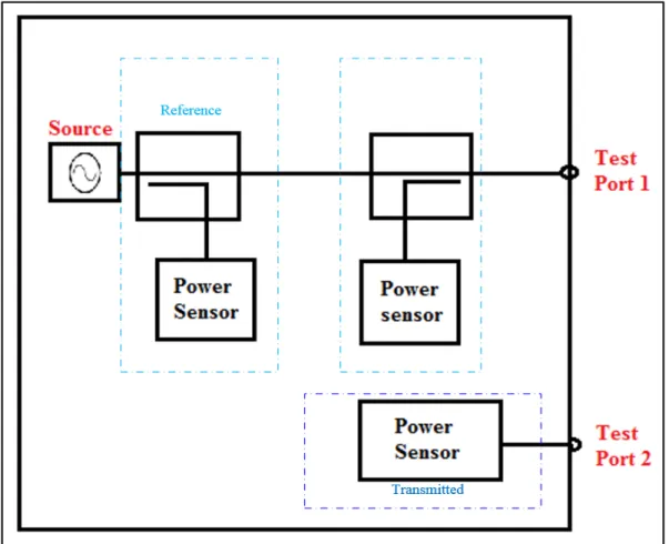
The six-port method, which has undergone continuous development and improvements, was introduced as a measurement technique by Engen and Hoer in 1970s to determine the amplitude and phase of RF signals based on four scalar power readings (F. M. Ghannouchi, A. Mohammadi, 2009). A six-port junction is the essential part of the six-port technique that is well-suited for low-complexity network analyzer tasks as an alternative to conventional VNAs. Figure 1.4 shows a typical six-port junction which contains two directional couplers to sample the incident and reflected waves (D1, D2), five power dividers (PD1 – PD5) a and hybrid coupler (Q).Four power detectors connected to ports 3 to 6 are used to measurefour
14
magnitudes that help in computing the complex reflection coefficient value for the device under test DUT (Y. Cassivi, and al, 1992).
Figure 1.4Six-port junction diagram taken from Y. Cassivi, and al( 1992, p.465)
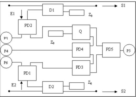
Because of the need to decrease the costof digital transceivers, several direct-conversion transceivers which used six-port technology are proposed in(C. A. Hoer, 1972), where simple techniques are usedfor measuring voltage, current, power, complex impedance, and phase angle utilizing a six-port coupler. The four side arms of this ideal six-port have output voltages proportional to the voltage as presented in Figure 1.5, current, incident voltage wave, and reflected voltage wave, respectively, all referred to some desired reference plane in the transmission line.
15
Figure 1.5Utilizing ideal hybrids, couplers, and voltage and current probes taken from C. A. Hoer(1972, p.468)
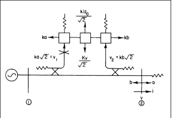
In (G. F. Engen and C. A. Hoer,1972), a six-port homodyne method employed power detectors rather than mixers as in Figure 1.6, resulting in less complex circuits compared to the traditional six-port heterodyne approach. The benefits of using the six-port homodyne receiver include ultra-low power consumption, less costly transceivers, and easily obtained broadband specifications from passive elements.
Figure 1.6Arbitrary six-port junction representation taken from G. F. Engen and C. A. Hoer(1972, p.471)
16
The RF circuit’s ultra-large frequency bandwidth is a crucial benefit of six-port design and the main reason why, in six-port transceiver architectures, it is used in applications such as ultra-wideband (UWB) systems and software-defined radio (C. A. Hoer,1977),the latest wireless applications. In (E. R. B. Hansson, G. P. Riblet, 1983), the researchers used a six-port transceiver at 60 GHz in CMOS technology, intending to develop a low-cost, low DC power-consuming miniature transceiver. The proposed transceiver in (E. R. B. Hansson, G. P. Riblet, 1983) showed total DC power consumption under 100 mW.
A new automobile radar based on the six-port phase/frequency discriminator where the block diagram of the proposed prototype as in Figure 1.7 includes microwave oscillator, modulator and the VCO, the six-port, which plays the role of a mixer., and power detectors are placed at outputs 3–6. The frequency of the four signals that go into the analog–to–digital (A/D) converter is the Doppler frequency of the target. This technique forces the modulation frequency to be the half of the sampling to ensure the Nyquist theorem; the sampling frequency should be at least the double of the highest frequency that is expected to measure (C. Gutierrez Miguelez, and al,2000).
Figure 1.7Block diagram of the proposed radar taken from C. Gutierrez Miguelez (2000, p.1417)
17
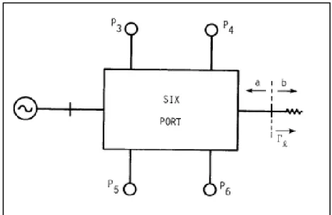
1.3.2 The Six-Port Reflectometer
A six-port reflectometer is a passive microwave six-port junction that allows the measurement of the complex reflection coefficient ratio of two RF signals using four power detector circuits (D3, D4, D5, D6) only, (G. F. Engen,1977).Figure 1.8 illustrates a block
diagram of a six-port reflectometer with a source connected at port 1 and the DUT connected at port 2.
Figure 1.8Block diagram of six-port reflectometer taken from G. F. Engen(1977, p.44).
The powers detected at ports P3-P6 are formulated in terms of reflected (b2) and forward (a2)
waves as follows (G. F. Engen,1977):
= |A ∗ a + B ∗ b | (1.1)
= |C ∗ a + D ∗ b | (1.2)
= |E ∗ a + F ∗ b | (1.3)
18
where A, B, C, D, E, F, G and H are complex constants specific to the six-port junction. Equations 1.1 to 1.4 can be reformulated in terms of the reflected power,|b2| , and the
unknown load reflection coefficientΓas:
=|A|2|b |2 |Γ − q3| (1.5) =|C|2|b |2 |Γ − q4| (1.6) =|E|2|b |2 |Γ − q5| (1.7) =|G|2|b |2 |Γ − q6| (1.8)
where: q3=-B/A, q4=-D/C, q5=-F/E, q6=-H/G.
In (G. F. Engen,1977), Engen introduced a design where port 3 is used as a reference port and is coupled to the reflectometer’s port 1 directly. Port 1, being the injection site for input power, is insensitive to port 2, being the origin of the reflected wave. Under these conditions, Equation 1.1 becomes:
= | B ∗ b | (1.9)
Using thepower at port 3 as a reference power to find the reflection coefficient, the powers (i.e., power ratios) at the other ports are normalized as follows: P4/P3, P5/P3, and P6/P3. Based
on this, we obtain the following equations:
=
| |19 5 3 = |Γ −q5|2 | |2 (1.11) 6 3 = |Γ −q6|2 | |2 (1.12)
In this form, it is clear that the ‘q’ points in Equations 1.10 to 1.12are the centres for three circles in the complex plane. If we define the radii of these circles as R4, R5 and R6, then
these equations can be re-written as:
=|Γ − q4| (1.13)
=|Γ − q5| (1.14)
=|Γ − q6| (1.15)
The unknown load reflection coefficient, ΓL, is then found by the intersection of these three
20
Figure 1.
9
Geometric impact of Equations1.10 – 1.15 in formulatingcomplex reflection coefficientstaken from G. F. Engen(1977, p.46)
By employing added detectors, the six-port approach can give a more cost-effective measurement for both phase and amplitude. At the same time, the six-port method can also provide more accurate power measurements as well as network parameters. Using the six-port method enables impedance and power flow measurements to be performed at the same time by utilizing the amplitude measurements (i.e., no need for phase measurements). Additionally, as demonstrated in (A. L. Samuel,1974), if one or two six-port configurations is/are used along with a suitable calibration and test-set strategy, they can measure the four scattering parameters for two-port DUTs. The six-point design can also be used for directional finding of received waveforms (A. Koelpin, al,2010). Other applications of the six-port technology are polarization and near-field antenna measurement and in the radar system, giving the desired high performance/low cost in lucrative fields such as the automotive industry (C. Nieh, T. Huang, and J. Lin,2014).
21
1.4 Phase and Gain Detection
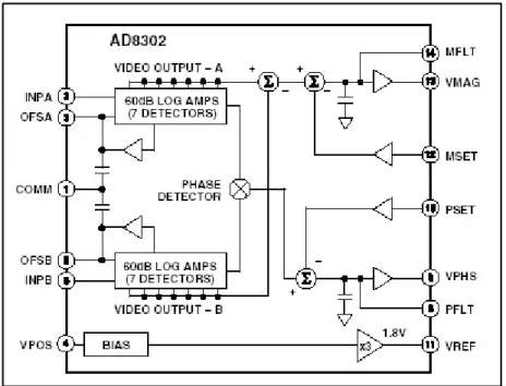
Dedicated gain and phase detection circuits offer another alternative solution for measuring the amplitude and phase of two RF signals. The AD8302 from Analog Devices (Analog Devices, 2002) is one such circuit that includes demodulating logarithmic amplifiers with 60 dB dynamic range as shown in Figure 1.10. So, by taking the difference between their outputs OFSA and OFSB, the magnitude ratio or gain between the input signals (INPA and INPB) can be gained. Further, it contains a phase detector of multiplier kind. The phase accuracy is not dependentof the level of signal over the large range. The AD8302 issues two voltages at the outputs VMAG and VPHS that are corresponding to the differences of gain and phase between the two measured branches. The practical block diagram of the AD8302 present in Figure 1.10 bellow:
Figure 1.10Functional photograph of the AD8302 taken from Analog Devices data sheet(2002, p.1)
It should be noted that the AD8302 requires the use the directional couplers to sample the waves, which increases the size and losses. Moreover, calibration at one of the inputs
(
INPA or INPB)as ACreference signalis requiredbefore carrying out measurements.22
1.5 Conclusion
This chapter presented different microwave scalar and vector measurement techniques. Starting from the best known technique widely used to measure the relative amplitude and phase of RF signal is vector network analyzer VNA. This VNA provides very high accuracyand wideband measurement over the frequency range. Because of the complexity of vector network analyzer, the six-port junction is an alternative technique that reduces the complexity of the measurements and provides the vector measurement by using couplers, dividers, mixers, and power detector circuits and other microwave components. Further, six-port technique reduces the complexity of six-six-port junction by using only couplers and power detector circuits as well as Gain and Phase detection circuit with 60 dB dynamic range. Despite all the advantages of these techniques; from accurate measurement and wide frequency range, all of these approaches are use the directional coupler for sampling reflected and incident waves. Due to size issues with the coupler, integrating it into an embedded system is impractical, especially at low frequencies. Moreover, this architecture would demand additional calibration efforts and necessitate a directional coupler and multiple dividers/hybrids, again making the design unsuitable for current and future needs and trends.
CHAPTER 2
PROPOSED REFLECTOMETER
Chapter 1 presented different alternative techniques for RF vector measurements using the directional couplers, which have the disadvantages of large size making them not suitable for circuit integration and embedded measurement. In this chapter, an alternative technique that is suitable for circuit integration and embedded measurement using a four-port reflectometer will be presented. The new optimized four port reflectometer will be descried and the theory for computing the reflection coefficient of the device under tests DUTs will be presented.
2.1 Related Work
In 2010, a novel design of four-port reflectometer was investigated(A. B. Kouki, et al., 2010). The reflectometer, see Figure 2.1, used (i) a microstripline (Signal-carrying line),where the RF source is connected at the input (port 1) and the device under test is connected to the output (port 2) of this signal-carrying line, (ii) two sniffers located close to the transmission line on the same layer and separated by the distance d, and (iii) two power detector circuits linked to the coupled ports 3 and 4 to measure the coupled power.
Basically, the sniffers are very simple structures that have very small size and provide very low coupling (below -30 dB). This makes the reflectometer more convenient for integration in microwave circuits to enable embedded measurement. Because of having a very low coupling factor, the sniffers will not have any effect on the propagation of the power signal in the system. However, having the sniffers in the shown planner arrangement, i.e., close to the signal-carrying traces, will impose restrictions on the circuit design and the routing of additional traces.
24
Figure 2.1Four-port reflectometer topology Taken from A. B. Kouki, et al., (2010, p.2) 2.2 Proposed 3D Four-Port Reflectometer Description
To avoid the above-mentioned limitations explicitly, the sniffer lines must be designed so that they do not intersect other signal lines. To accomplish this, we proposed to perform signal sniffing differently. The proposed reflectometer uses new sniffers which are made of partially filled vertical vias in 3D placed under the signal carrying transmission line. In this manner, the surface of the circuit is freed from any complex routing of lines. Furthermore, these sniffers offereven more size reduction and are very well suited for circuit integration and embedded measurement.
Figure 2.2 illustrates the proposed structure where port 1 of the transmission line is connected to the RF input power while port 2 of the transmission serves to connect the DUT. Thetwo sniffers are placed a distance d apart underneath of the transmission line in a 3D form to couple very small portions(-30 dB) of the companied forward and backward signals. These sniffers are connected to two power detector circuits, LT5582 (Analog Devices, 2010-2018),for power measurement at ports 3 and 4 through a buried line.To route the sniffed signals to the surface of the circuit at its edges, transitions are needed. The design of these transitions uses vertical vias as shown in Figure 2.3 which are typically highly inductive.
25
Therefore, careful compensation of these transitions is required to keep a matched impedance from the sniffers to the surface lines.
Figure 2.2The block diagram of proposed 3D four-port reflectometer
26
2.3 Reflection Coefficient Determination
First, we assume that the S-parameters of the reflectometer are known. This can be accomplished by 3D field simulation of the reflectometer geometry or from measurement of the fabricated reflectometer prototype. Referring to Figure 2.1, the reflection coefficient of the DUT at port 2 is given by:
2 2 L
a
b
=Γ
(2.1)Further, the measured powers at ports 3 and 4 are given in terms of the waves b3 and b4 as
follows (assuming well matched ports):
2 3
b
3P
= (2.2) 2 4b
4P
= (2.3)Next, we determine the transmission coefficients from port 1 to port 3, T31, and to port 4, T41.
Using signal flow graph analysis and Mason’s rule (G. Gonzales, 1977), (A. B. Kouki, et al., 2010) the following expressions in terms of the reflectometer’s S-parameters can be obtained: 3 32 21 32 21 31 22 31 31 31 1 22 22 ( ) 1 1 L L L L
b
S
S S
S S
S S
S
T
=a
= +S
= −S
+ −Γ
Γ
−Γ
+Γ
, where , =0 (2.4) 4 42 21 42 21 41 22 41 41 41 1 22 22 ( ) 1 1 L L L Lb
S
S S
S S
S S
S
T
=a
= +S
= −S
+ −Γ
Γ
−Γ
+Γ
, where , =0 (2.5)27
The S-parameters in the equations (2.4) and (2.5) can be grouped using six new variables, A1,
A2, B1, B2, C, and D as: 21 32 31 22 21 42 41 22 1 2 31 1 2 41 22 ( ) ( ) 1 C D
S S
S S
S S
S S
A A
S
S
B B
S
− − = − (2.6)Then and can be rewritten explicitly in terms of these known new variables and the unknown DUT’s reflection coefficient as:
1 1 3 31 1 1
1
L LA
B
b
X
T
C
D
a
a
Γ +
=
=
Γ +
(2.7) 4 2 2 41 1 11
L Lb
A
B
X
T
C
D
a
a
Γ +
=
=
Γ +
(2.8)By using equations (2.7) and (2.8) in equations (2.2) and (2.3), the measured power at ports 3 and 4 can be written as:
1 2 3 1 1 L L
A
B
D
P P
C
+
=
Γ
Γ +
(2.9) 2 2 4 1 2 L LA
B
D
P P
C
+
=
Γ
Γ +
(2.10)28
Writing ΓL= x+jy, equations (2.9) and (2.10) can be written as:
2 2 2 3 3
(
3)
(
x
−
α
)
+ −
y
β
=
r
(2.11) 2 2 2 4 4(
4)
(
x
−
α
)
+
y
−
β
=
r
(2.12)where
α
3,
β3, α
4,
β4,r
3, and r4 are six complex parameters which are expressed interms of A1,B1, A2, B2, C, D, and P1, all known quantities. These parameters are given by:
31 1 1 1 1 2 2 2 2 3 31 1 1 ) ( ) ( ) ( )
(
r r i i r r i i r i r iD C
D
C
P
B A B A
C C
P
A A
α
= − + − + + − + , (2.13) 31 1 1 1 1 2 2 2 2 3 31 1 1 ) ( ) ( ) ( )(
i r r i i r r i r i r iD C
D
C
P
B A B A
C C
P
A A
β
= − − − − + − + , (2.14) 2 2 2 2 1 1 31 2 3 2 2 2 2 2 31 1 1 3 3 ( ) ( ) ( ) ( ) i r r i r i r i sqrtB B
D D P
r
C C
P
A A
α
β
+ − + = + − + + + , (2.15) 41 2 2 2 2 2 2 2 2 4 41 2 2 ) ( ) ( ) ( )(
r r i i r r i i r i r iD C
D
C
P
B A B A
C C
P
A A
α
= − + − + + − + , (2.16) 41 2 2 2 2 2 2 2 2 4 41 2 2 ) ( ) ( ) ( )(
i r r i i r r i r i r iD C
D
C
P
B A B A
C C
P
A A
β
= − − − − + − + , (2.17)29 2 2 2 2 2 2 41 2 4 2 2 2 2 2 41 2 2 4 4 ( ) ( ) ( ) ( ) i r r i r i r i sqrt
B B
D D P
r
C C
P
A
A
α
β
+ − + = + − + + + , (2.18)Equations (2.11) and (2.12) represent two circles in the complex plane centered at Q3of
coordinates (α3, β3) and Q4of coordinates (α4, β4) and or radii r3 and r4, respectively. The
solution to these equations can be found graphically by finding the intersection between the two circles as shown in Figure 2.4. The existence and the positionsof the two intersecting points depend on the distance d that is separating the two sniffers. Additionally, of the two intersections one will be inside the unit circle on complex Γ plane while the other one will be outside of the circle as seen in Figure 2.4. For passive loads, the following condition must be met, which means that only the intersection point inside the unit circle is retained as a solution:
2 2 2
1
L= +
x
y
≤
Γ
(2.19)Figure 2.4Two circles intersection in the complex plane todefine the reflection coefficient (Γ)
CHAPTER 3
PROPOSED REFLECTOMETER
In this chapter, the proposed 3D four-port reflectometer will be implemented. The frequency of operation is chosen to be 1.2 GHz. The reflectometeris first simulated using a 3D electromagnetic field simulator HFSS and later fabricated in low temperature co-fired ceramics (LTCC) using four layers of Ferro L8 substrate as seen in Figure 3.1. Table 1 summarizes the main characteristics of the substrate used.
Figure 3.1illustrates the details of the stack of layers used throughout this chapter.
Table 3.1Ferro L8 characteristics
Parameters Values
Dielectric Constant 7.2
Loss tangent 0.002 @ 1.2 GHz
32
3.1 Microstripline Design and Simulation
First, a microstripline will be designed to connect the source at port 1 and the device under test at port 2. Itswidth (W), as shown in Figure 3.2, can be calculated using the formulas in (David M. Pozar, 2011) below:
(3.1) where: 0 1 1(0.23 0.11) 60 2 1 r r r r Z A
ε
ε
ε
ε
+ − = + + + (3.2) 0 377 2 r B Z πε
= (3.3)33
However, instead of using the above equations, the LineCalc tool in Advanced Design System ADS, see Figure 3.3, is used to compute the dimensions of a 50 Ω transmission line (Width, Length) on the Ferro L8 substrate with the characteristics given in Table 3.1.
Figure 3.3LineCalc calculator layout
Once the microstripline is dimensioned, we built its 3D model for simulation. Figure 3.4 shows the designed microstripline in the3D high frequency simulator system HFSS, which is 3D electromagnetic simulation. The dimensions used are: 853 um in width and a length of 15 mm with a substrate thickness of 653 um. The first HFSS simulations confirm that this line is indeed a 50 Ω line. The next step is to introduce the sniffers under this transmission line in a 3D structure. This will be detailed in the following section.
34
Figure 3.4Microstripline design in HFSS. 3.2 Sniffer Design
The aim of using sniffers, as explained in chapter 2, is to couple a small portion of the incident and reflected signals’ power in order to measure the reflection coefficient of the device under test. These sniffers could be in different shapes and at different positions, like planner sniffers in (A. B. Kouki, et al., 2010) where the sniffers were located close to the transmission line TL on top of the substrate. Similarly, they could be close under the transmission line in a vertical position through the LTCC layers as we propose to do in our 3D reflectometerdesign. This can be achieved by using vias that are filled in several layers beneath the line without touching it. Cylindrical and rectangular vias are two kinds of vias that can be easily used to this end. Both types were simulated and their performance was found to be comparable. The diameter of the cylindrical via was 136.8 um while the rectangular vias measured 144.8um x 88.9 um, as shown in Figure 3.5. The viaswere centered under the microstripline with a vertical spacing of 127 um, which corresponds to the thickness of one layer. The coupling level was found to be -30 dB.As expected, it was found that the vertical spacing between the sniffer (vias) and the microstripline determines the amount of coupling that can be achieved. Therefore, depending on how much signal coupling
35
is needed, the thickness and number of layers that do not include vias can be adjusted to meet the desired coupling level.
Figure 3.5(a) cylindrecal via (b) rectangular via
To route the sniffed signals from underneath the microstripline to the surface of the circuit where power detectors can be mounted, a buried transmission line with a transition to the surface of the circuit are needed. These must be carefully designed to maintain good impedance matching.
3.3 Perpendicular Transition Design
Figure 3.6 illustrates the geometry of the proposed transition design. It consists of a buried line (SL) connected to a surface microstrip line (ML) through a center via of 150 um diameter. The characteristic impedance of the buried line can easily be controlled by its width and does not pose a challenge in the design. However, the center via being much
36
smaller in diameter that the MS line width will introduce an inductive discontinuity that will cause impedance mismatch at the power detection ports. Therefore, this discontinuity must be compensated through the use of the additional grounded vias that surround the center via. All grounded vias have a diameter of 150 um. This structure approximates a vertical coaxial line whose characteristic impedance can be tuned by controlling the distance between the grounded and center vias.
Figure 3.6Perpendicular transition models in HFSS
The proposed vertical transition structure uses Ferro L8 substrate that has dielectric constant of 7.2 has the thickness of 635 um. All the grounded vias are connected to the ground plane which is located at the bottom of the last layer of the substrate. The width of the microstripline is W1= 853 um and that of the buried line is W2= 127 um as well as the height from the buried line to the grounded via was equal to 127 um as seen in Figure 3.1, The height of all vias is 508 um and the distance between the center via and the grounded (veil) vias is 1000 um. These dimensions have been optimized in order to obtain a coaxial line where the signal transmits according to TEM mode between the inner and outer connector. Figures 3.7 and 3.8 present the side and top views, respectively, of the proposed transition.
37
Figure 3.7Side view of vertical transition. D1=508 um and D2=127 um
Figure 3.8Top view of the vertical transition with W1=853 um, W2=127 um, dv =150um,D1=1000 um
38
3.4 3D Four-Port Reflectometer: Version 1
By combining the micostripline,the sniffers and the vertical transition, a new 3D 4-port reflectometer can be created with small size, low-cost, and ease of integration for embedded vector (amplitude and phase) measurement with good measurement accuracy and with no interfering between the sniffers and other transmission lines. Further, because of the simple structure of the sniffers, we can place them at any distance that is less than 4. So, we are able to design different structures of reflectometers with different spacing between the sniffersin order to obtain a vector measurement for different frequencies and applications. Figure 3.9a,b,c, d present the final design of the proposed reflectometer with different spacing (d) expressed in wavelength. For the four designs shown, the spacing between the sniffers sit at 11, 20, 25, 40.
39
3.4.1 EM Simulation
The ANSYS HFSS is a 3D electromagnetic (EM) simulation for designing and simulating high- frequency electronic products such as antennas, antenna arrays. This simulator is used to compute the S-parameters of the proposed complete 3D reflectometer shown in Figure 3.9.
Our focus is onobtaining good matching at all ports with less than -20 dB reflection coefficient for S11 and S22, a low coupling less than – 30 dB for S31 and S41. The simulation
results show that S11 and S22 for all structures are below -20 dB and that the insertion loss,
S21, is -0.1 dB as seen in Figure 3.1a,Similarly, S31 and S41in Figure 3.10b show low coupling
around -30 dB, which is the coupling that we are expected to get at the coupling ports of the proposed reflectometer to measure the output coupled power.
Figure 3.10(a) simulated S11 and S22 in dB, (b) simulated S31 and S41 in dB 3.4.2 Fabrication in LTCC Technology
The proposed reflectometer has been fabricated on low temperature co-fired ceramics (LTCC) substrate, which has advantages of low cost, high performance and the availability of a wide range of materials, such as Ferro A6 and Ferro L8. To fabricate our designed structure, Ferro L8 material is used. We usedthree layers of 10 mils thick sheets and one 5
40
mil-thick sheet in the stack. We also used silver paste to fill the vias and to print the microstrip and buried lines.
The fabrication process proceeded as follows. First, the process is started with via punching on each single sheet, then via filling by the silver paste followed by printing the lines on the proper sheets. The next step was stacking all the sheets together to get a single stack. Because we included different designs on one 10 cm x 10 cm stack, cutting was the necessary next step to separate the designs into individual pieces. After that, the last step consisted of co-firing the cut pieces into the oven between 4 to 6 hours following a specified temperature profile with a maximum of875 . Figure 3.11 shows different fabricated prototypes of the final proposed 3D four-port reflectometer configurations.
41
3.4.3 S-Parameters Measurement of the 3D 4-port Reflectometer
In order to measure the parameters of a multi-port network, waves must be inserted at the a selected port while each of the other portsisterminated by a matched load equal to system’sreference impedance Zo (usually 50 Ω). For a two-port network, the explicit definitions and measurement conditions of the S-parameters are as follows:
= ℎ 2 = 0 = 1 (3.4)
= ℎ 2 = 0 = 1 2 (3.5)
= ℎ 1 = 0 = 2 1 (3.6)
= ℎ 1 = 0 = 2 (3.7)
It is worth noting that every parameter is a complex quantity. So, for instance, the angle indicates phase difference in degrees, whereas the magnitude indicates the ratio between the amplitudes in dB (David M. Pozar, 1998).
= | | (3.8)
) = 20 log | | (3.9)
The fundamental of vector network analyzers (VNAs) has been covered in chapter 2 as one of the techniques that measures the amplitude and phase of signal ratios. The use of a VNA requires a calibration prior to measuring devices. A full two-port calibration procedure is used to calibrate the Agilent HP8753ES VNA used to measure our reflectometer prototypes. This calibration is based on the SOLT (Short-Open-Load-Through) technique which achievescorrection for cable length and loss and all internal instrument impairments. The
42
calibration standards used are those of the 85052D 3.5 mm calibration kit. Calibration was carried out between 1 and 1.4 GHz with the center frequency being our design frequency, namely 1.2 GHz.
The S-parameters of the fabricated prototype were obtained using the vector network analyzer VNA(Agilent HP8753ES) with the input power range of -5 t0 -10 dBm over the frequency range of 1 GHz to 1.4 GHz. Since this VNA has only two ports, multiple connections and measurements were carried out sequentially by connecting the VNA to two of the ports and terminating the others with 50 Ω termination loads as shown in Figure 3.12.
Figure 3.12S-parameters measurementsetup of the fabricatedreflectometer prototype using a commercial VNA
The measured S-parametersof the proposed prototype are presented in Figure 3.13 The measured return losses RL of the prototype are marked around -15 dB which is higher than the simulation results. However, the measured coupling at ports 3 and 4 are around -30 dB as
43
predicted in simulation. The lack of good RL levels will have an impact on the precision of the measurements using the reflectometer and will be further addressed in section 3.5 where a second improved version of the reflectometer is proposed.
Figure 3.13Measured S-parameters of the 4-port reflectometer 3.4.4 Coupled PowerMeasurement using Power Meter
The power meter is an instrument that is used to measure an RF signal’s power with high precision and over wide frequency ranges and power levels. In the previous work (A. B. Kouki, et al., 2010), power meters were used to measure the output power at port 3 and 4, namely P3 and P4, which are then used in equations 2.11 and 2.12 to determine the complex reflection coefficient. Here, we propose to also use power meters as first step and more easily integrable power detectors at a second step. To this end, an external Agilent E4417A power meter is connected to port 3 and 4. Next, a 0 dBm power input signal is injected at port 1 while several different loads (DUTs) are connected at port 2 and the power meter readings at ports 3 and 4 are noted. This is repeated for three different frequencies, namely 1, 1.2, and
44
1.4 GHz. Table 3.2 summarizes the obtained measurements when DUT is a 50 Ω matched load.
Table 3.2 Coupled power measurement using theE4417A power meter with 0 dBm input power and 50 Ω termination different frequencies.
Loads Frequency Input power
P3dBm P4dBm
50 Ohm 1 GHz 0 dBm -27.989 -27.643
50 Ohm 1.2 GHz 0 dBm -27.513 -27.556
50 Ohm 1.4 GHz 0 dBm -27.413 -27.388
3.4.5 Coupled PowerMeasurement using the LT5582 Power Detector Circuit
The need for the integration to achieve small size and low cost embedded RF measurements means that power meters are not an option for power measurement. Indeed, the power meter is still an external instrument that cannot be integrated for embedded measurement. Therefore, we consider the alternative of using a power detector chip instead. The LT5582 RMS power detector, from Analog Devices, is capable for measuring the RMS power and has been used for several applications such as PA power control and receiving and transmitting gain control. Also, it has the features of the small size of the circuit which is 3 mmx3 mm and a dynamic range of 57 dB. It also shows low linearity error over its entire dynamic range and covers a wide frequency range from 40 MHz up to 10 GHz. Figure 3.14a presents the circuit schematic from the data sheet with the LTC5582 IC and different resistors and capacitors at the input and the output of the circuit. This detector requires a 3.3V supply voltage, a 3.3V enable voltage, and can has a maximum input power of 18dBm. It is rated to operate between-400 C to 850 C. A prototype of this detector was designed,
following the company’s reference design, and fabricated on a Rogers’s substrate with dielectric constant 6.15 as shown Figure 3.14b. This design can be easily be implemented in LTCC as a step to reach the full circuit integration with the proposed reflectometer.
45
Figure 3.14(a) Shows the LTC5582 circuit from the datasheet(b) LTC5582 fabricated circuit on Roger Substrate
In order to examine and test the fabricated circuit, we first characterize the detector response. To do this, the input of the circuit is connected to a signal generator which injects different input power levels while the output port is connected to an oscilloscope which reads the output voltage. This test setup is presented in Figure 3.15. The graph in Figure 3.10ashows the output voltage response versus the input power from the data sheet with linear response of the input power until -57 dBm for several frequencies between 450 MHz and 5.8 GHz. The graph in Figure 3.10b presented the measured response of the fabricated prototype for a similar power range at 1.2 GHz. The obtained result is quasi-linear which confirms that the fabricated circuit can operate close to the manufacturer’s specifications.
With the basic detector circuit characterized and validated, next we produce two detector circuits and connect them to the coupling ports 3 and 4 of the reflectometer. Again, we apply a 0 dBm RF signal at input port (port 1) and place a 50 Ω termination load at the output port (Port 2). Table 3.3is sumurizes thecoupling measurement using the LTC5582 power detector circuits with 0 dBm input power at different frequencies. These results are similar to those obtained using power meter measurements. It is therefore possible to use the LTC5582 power detector circuits at different frequencies without loss of accuracy in measurements.
46
Figure 3.15Test setup to characterize the fabricated LTC5582 power detector
Figure 3.16(a)Output Voltage vs RF Input Power (data sheet), (b) The measured output voltage vs input power for
47
Table 3.3Coupling measurement using LTC5582 power Detector circuits with o dB input power at different frequencies
Loads Frequency Input power
P3dBm P4dBm
50 Ohm 1 GHz 0 dBm -27.987 -27.621
50 Ohm 1.2 GHz 0 dBm -27.523 -27.546
50 Ohm 1.4 GHz 0 dBm -27.410 -27.375
3.4.6 Reflection Coefficient Measurement
At this stage, we are reaching at the last step of our research problem which is the validation of the theory in chapter 2 and the feasibility of the proposed 3D reflectometer as an embedded measurement circuit. To do this, we need to measure reflection coefficients of different loads using both the commercial VNA and our 3D reflectometer with the LTC5582 power detectors. To generate different load impedances, we use a double stub tuner with one port terminated by a 50 Ω load and other port connected to the VNA, as shown in Figure 3.17. We start with the VNA measurements at 1.2 GHz for a set of different loads corresponding to different double stub settings. In all 45 different loads are generated and measured.
48
Figure 3.17Test setup for reflection coefficient measurement using a VNA
Second, we perform similar measurements using the proposed reflectometer with 0 dBm RF input power injected in port 1, while the manual double stub tuner is connected to port 2 as shown in Figure 3.18. The same double stub tuner settings for the 45 loads used with the VNA are repeated for the reflectometer.
49