HAL Id: tel-02295386
https://tel.archives-ouvertes.fr/tel-02295386
Submitted on 24 Sep 2019
HAL is a multi-disciplinary open access archive for the deposit and dissemination of sci-entific research documents, whether they are pub-lished or not. The documents may come from teaching and research institutions in France or abroad, or from public or private research centers.
L’archive ouverte pluridisciplinaire HAL, est destinée au dépôt et à la diffusion de documents scientifiques de niveau recherche, publiés ou non, émanant des établissements d’enseignement et de recherche français ou étrangers, des laboratoires publics ou privés.
Optical antennas for harvesting solar radiation energy
Waleed Tariq Sethi
To cite this version:
Waleed Tariq Sethi. Optical antennas for harvesting solar radiation energy. Electronics. Université Rennes 1, 2018. English. �NNT : 2018REN1S129�. �tel-02295386�
THÈSE / UNIVERSITÉ DE RENNES 1
sous le sceau de l’Université Bretagne Loirepour le grade de
DOCTEUR DE L’UNIVERSITÉ DE RENNES 1
Mention : Traitement de Signal et TélécommunicationsWaleed Tariq Sethi
préparée à l’unité de recherche IETR (UMR 6164)
(Institut d’Electronique et de Télécommunications de Rennes UFR
Informatique et Electronique
Optical antennas
for harvesting solar
radiation energy
Thèse soutenue à Rennes le 16 Février 2018
devant le jury composé de :
Guillaume Ducournau
IEMN Université Lille 1 / Polytech'Lille, France / rapporteur
Paola Russo
Università Politecnica delle Marche Ancona, Italy / rapporteur
Olivier Pascal
Université Paul Sabatier, France / examinateur
Mohamed Himdi
Université de Rennes 1, Rennes, France / directeur de thèse
Hamsakutty Vettikalladi
King Saud Université, Saudi Arabia
Habib Fathallah
Université de Carthage, Tunisie
Ecole doctorale MathSTIC
Table of Contents
Acknowledgments i
Chapter 1 General Introduction..……….1
1.1 Introduction to Energy Harvesting ...1
1.2 Photovoltaic solar harvesting vs Radio Frequency energy harvesting ...2
1.3 Plasmonics and Surface Plasmons ...5
1.4 Context and motivation of the study ...7
1.5 Objectives and research contributions ...8
1.6 Thesis Structure ...9
Bibiliography ...11
Chapter 2 Radio Frequency Energy Harvesting Rectenna 12
2.1 Introduction to Radio Frequency (RF) Energy Harvesting ...12
2.2 Radio Frequency (RF) Energy Harvesting Principle ...13
2.2.1 Antenna ...14
2.2.2 Impedance matching cricuit ...15
2.2.3 Rectifier ...16
2.3 Literature Review: State-of-the-art Energy Harvesting Rectennas ...18
2.4 Proposed Hexaband antenna ...28
2.4.1 Antenna Design ...28
2.4.2 Antenna Simulation and Experimental Results ...29
2.5 Proposed multiband rectifier ...33
2.5.1 Schottky Diode Selection ...34
2.5.2 Impedacne matching ...35
2.5.3 Complete Rectifier in ADS Simulator ...35
2.6 Experimental Investigation of Rectenna System ...46
2.7 Summary and conclusion ...49
Bibliography ...50
Chapter 3 Optical Antennas based on Dielectric Resonators (DR) 52
3.1 Introduction to Optical Antennas/ Nantennas ...52
3.2.1 Optical Properties of Metals (Drude Model) ...58
3.3 Brief Introduction to Surface Plasmons Polaritons (SPP) and Local Surface Polaritons (LSP) ...61
3.3.1 Localized Surface Plasmons (LSP) ...62
3.4 Literature Review: Dielectric Resonator (DR) Based Nantennas ...63
3.5 Proposed Equilateral Triangular Dielectric Resonator Nantenna [ETDRN] ...65
3.5.1 Introduction to Dielectric Resonator antenna (DRA) ...65
3.5.2 ETDRN Design Geometry ...66
3.5.3 Antenna Simulation and Experimental Results ...67
3.5.4 Results and Discussion ...73
3.6 Proposed Hexagonal Dielectric Resonator Nantenna [HDRN] ...75
3.6.1 HDRN Design Geometry ...75
3.6.2 Design Simulation and Optimisation ...77
3.6.3 Results and Discussion ...80
3.7 Array synthesis ...84
3.7.1 Antenna Array Design Geometry ...84
3.7.2 Results and Discussion ...85
3.7.3 Tuneability of proposed 1x2 ETDRNA Array ...87
3.8 Summary and conclusion ...90
3.9 Bibliography ...91
Chapter 4 Proposed optical antennas for harvesting infrared energy 94
4.1 Introduction to Optical Photodetectors (PD) ...94
4.2 Optical Photodetector for THz detection ...96
4.3 Optical Antenna Design I: Yagi-uda Antenna with Fermionics Photodiode ...99
4.3.1 Molybdenum based Yagi-uda Antenna Design ...99
4.3.2 Simulation and measurements of proposed yagi-uda nantenna ...102
4.3.3 Aluminium based Yagi-uda Antenna Designs ...105
(a) Antenna Design with Aluminium Material ...105
(b) Array Design with Aluminium Material ...109
(c) Experimental realization of Yagi-uda Nantenna Array Aluminium Material ...115
4.4.1 PDMS based Lens Antenna Design ...121
(a) PDMS Polymer ...121
(b) Lens Antenna Design Simulations ...122
4.5 Optical Antenna Design III: Thermopiles Antennas ...125
4.5.1 Thermopile antenna detector and geometric design ...125
(a) Principle of thermocouples ...125
(b) Proposed geometric designs and experimental realization: ...127
4.6 Summary and conclusion ...136
Bibliography ...137
Chapter 5 Conclusion, challengesa nd future work 139
5.1 Summary of Contributions ...139
5.2 Challenges faced during research ...141
5.3 Future Work ...143 List of Publications 144 List of Figures 145 List of Tables 150 Abstract 151 Résumé 152
1 | P a g e
Chapter 1
General Introduction
This chapter provides a brief introduction to energy harvesting, its various types and its current importance among the research community. Also a comparison between available photovoltaic harvesting to newly proposed radio frequency harvesting is mentioned. In section 1.3, basics to surface plasmons is given which leads to the motivation of the research work as presented in section 1.4. The objectives and contributions of this work with the layout of the thesis documentation is given in the remaining sections.
1.1 Introduction to Energy Harvesting
Over the last few years, worldwide demand for energy has increased by 50 % [1]. Although dependency of the worlds’ power is still on the combustion of fossil fuels yet, they are finite and cause environmental hazardous to our planet. An alternate clean renewable sources of energy are required that can fulfill the demands and save our planet in the process. Such solutions are possible either from using nuclear based fission reactions or capturing energy from artificial ambient sources such solar or wind. The former, although offers long lifetime, but it comes with its own dangers, however the artificial ambient sources can be utilized as they are technology based. Various external energy include mechanical vibration, thermal, wind, and Radio Frequency (RF) sources.
The process of collecting the energy from the ambient surroundings and converting it into useable electrical energy is termed as Energy Harvesting (EH). Such sources of energy can be scavenged from man-made devices or from natural available sources [2]. Man-made sources are abundant and they do not harm the environment. With the increase in technological devices mostly for wireless communication, the lifetime of devices needs to increase as well. Batteries that are mostly used as a source of energy for these devices need to be made operationally prolong. One solution is to use the available energy surrounding these devices in the form of radio frequency electromagnetic radiation and convert those abundant energies into a secondary source for these batteries. Hence, momentum in charging of batteries or even battery less systems have recently gained popularity [3–4]. The recharge period for batteries last almost ten years and we need a novel solution to enhance their lifetime. With the increase in wireless devices, which are battery dependent, we need a solution that can cope with the lifetime of these batteries. Energy harvesting offers a solution that can provide uninterrupted power to many applications near and far needed in this modern day and age of wireless communication. The applications for charging or storing energy can vary from monitoring weather stations to traffic control or charging medical implantation devices and cell phones. [5].
2 | P a g e
1.2 Photovoltaic solar harvesting vs Radio Frequency energy harvesting
The most direct and abundant source of energy comes from the Sun. From figure 1.1 it can be seen that the energy which is received on Earth can be divided into; 51 % of which is available at the Earth's surface that can be utilized for various tasks. The heat or energy form the Sun is used to lower the atmosphere temperature or heat its surface, melt the glaciers and then evaporate the water causing rain to appear and provide plants with necessary photosynthesis. Of the remaining 49% energy, reflected back energy is 4%, scattered via particles and clouds is 26% and the gases in the air absorb 19 % of the energy [6]. The solar energy that lies in the visible spectrum, as shown in figure 1.2, is being converted into useable electrical energy by a well-known technology. This technology is based on Photovoltaic (PV) effect which has matured over the years (since mid-70s). From the first silicon based cells to the second and third generation of photovoltaic cells which are based on thin film and multi-junction cells, a tradeoff has been standardized in the market as listed in Table 1.1, providing efficiency compared to its market cost.PV Technology Efficiency Market Captured
1st generation 20 90
2nd generation 5-12 10
3rd generation 40-50 10
Table 1.1 Efficiency of PV technology over the years [8]
Photovoltaic (PV) technology encompasses a basic element that is called a photovoltaic cell. The placement of these cells determine what is needed at the output. If photogenerated current is needed then the cells are aligned in parallel configuration. For maximum voltage to be seen at the output, series configuration is preferred. Photovoltaic cells worked on the principle of photo-electric effect, first discovered in 1839 by Alexander-Edmond Becquerel. The basic principle is the same as photo-electric effect which is based on interaction of photons having energy hv with electrons. As shown in figure 1.3, a typical PV cell is made from a semiconductor material. The photoelectric effect occurs in the center of the cell at the junction of two semiconductors. When the light is incident on the PV cell, photons interact with electrons in the valence band of the semiconductor. The photon and its energy is absorbed by the electrons, thus jumping to the conduction band while leaving a vacancy in the valence band in the form of a hole. This whole process is known as photo generation or an electron-hole pair generation which only happens if the energy of the photons are greater or equal to the band gap energy (energy gap between valence and conduction band). The newly created electron-hole pairs by photogeneration process are then driven by the electric field to the depletion region of the PN junction. Here the photovoltage and its subsequent photocurrent is generated when an electric load is connected to the PV cell.
As mentioned earlier, the energy received from the sun on the photovoltaics is utilized in visible region during the day time. At night the energy that is absorbed is not utilized by the solar cells. This released energy at night lies in the infrared region (IR) i.e. 7-17μm spectral range [7] along with some other infrared sources i.e. thermal engines and furnaces. In order to harvest and convert this available infrared energy into something useful as charging devices or batteries, we need some novel capturing devices and conversion electronics that can cope with the generated photovoltaic current technology.
3 | P a g e
One solution that can utilize this abundant IR energy released from the Earth’s surface is to make use of energy harvesting based on Radio Frequency (RF) techniques called rectennas. Rectennas working principle involves two components; (1) an antenna and (2) a rectifier circuit element. The antenna will work following its main principle of operation [9], i.e., receiving electromagnetic waves and resonating at desired frequency bands as per transmission lines or conducting elements shape. The rectifier will then take those alternating currents, pass through some diodes and give results in DC voltages [10]. All these steps will be accomplished keeping the impedance matching check between the antenna and diode. Rectennas offer an alternative and cheap solution to the already existing mature photovoltaics. Table 1.2 shows the comparison difference between both technologies;
4 | P a g e
Figure 1.2 Solar radiation spectrum: Top of the Earth's atmosphere and at sea level [7]
5 | P a g e
Table 1.2 Comparison between two technologies [11]
1.3 Plasmonics and Surface Plasmons
Harvesting energy in the IR domain requires understanding of how the electrons will operate in the antenna designed at the nanoscale. With the advancements in nano technology fabrication, different theories and ideas are surfaced and new fields of study are created that explain these phenomena. One such field of study, which is a branch of nano-photonics, is Plasmonics [12]. Plasmonics deal with the interaction of light with free electrons at the surface of Noble metals. It explains the generation, manipulation and detection of surface plasmon polaritons (SPP), which are quasi particles, appearing due to coupling of light with surface plasmons on the surface of metal and insulator interaction. Simply put, the most common definition of a Plasmon is; “A
plasmon is a quantum of plasma oscillation”. The requirement for a plasmon to get excitation is
when an electron passes through a thin film or gets reflected from the surface of a metal. This excitation can be seen from figure 1.4 where an incident electron is interacting with a thin film generating scattered electrons from the thin films surface along with two or more plasmons with hypothetical energies as ;
Electron incident energy ~ 1-10 KeV Plasmon energy: ~ 10 eV
Figure 1.4 shows a thin metal film where a beam of monochromatic light is projected onto to it with the help of a prism at certain angles of incidence i.e. between critical angle and θc and 90 degrees, where total internal reflection occurs. In this process, an evanescent waves (oscillating electric or magnetic field that tend to vanish exponentially and do not propagate far from the source) is produced. These evanescent waves tend to excite the electrons on the surface of the thin metal film that produces a phenomenon known as surface plasmon polaritons (SPP). With the mentioned angles on incidences, the wavelength of SPP’s coincide with eh wavelength of
Photovoltaic Rectenna
Efficiency Single cell produces 41%. Multiple junctions give 87%.
Theoretical limit is around 85%. Practically efficiency is more than 75%. Pros Well established and mature
technology.
Less fabrication issues.
Basic knowledge of rectification.
Fabrication using standard dielectric substrates. One time spending which is around 10 $. Cons Temperature dependent
performance.
Costly for multiple junctions.
6 | P a g e
evanescent waves thus producing resonances at the boundary of the metal sheet. The SPP’s produced are intensified with the energy received form the incident light source. To explain the working of the SPP’s, an enlarged or zoomed view is shown in figure 1.4. When electron oscillations (white dots) happen on the surface of the thin metals film, interaction of photons from light waves interact with them causing production of plasmons. Also, electromagnetic field oscillation is induced near the surface in synchronization with the surface plasmons. The SPPs are quasiparticles resulting from coupling between surface plasmons and electromagnetic waves [13]. The first known application of this photon electron interaction was documented to the Roman Empire with the use of metal particles in colored glass. A practical example of this can be seen at the British museum in London where a glass is forged into a chalice in the fourth century. It describes story of the mythological King Lycurgus being trapped by a vine after he attacked the god; Dionysus (figure 1.5). The amazing thing about this cup which makes it unique than other utensils is the way it interacts with light waves. In natural ambience, the cup shines green/jade but when light is shine through it, it glows bright red. This remarkable feature exists due to the presence of small portions of silver and gold about 70 n min diameter embedded in the glass cup. At this scale, the interaction of light with these noble metals cause a change in color due to a phenomenon known as surface plasmons. Surface plasmons appear and cause a change in color when the photons in the light interact with the electrons available on the surface of the material [14]. Innovation in nanofabrication technology and modelling of near filed electromagnetics have introduced a pace in the research domain of Plasmonics. Last decade has seen an enormous growth in the field of plasmonic resonances where its applications can be utilized in the field of quantum electrodynamics and the interaction between metals and light particles for harvesting solar radiation energy.
7 | P a g e
1.4 Context and motivation of the study
Recent years have witnessed an increased interest by the scientific community to acquire green and clean renewable sources of energy compared to traditional fossil fuels. One abundant source of renewable energy is the solar radiation which is applied currently for various applications [15]. There are generally two different ways in which solar energy is used – heat and electricity. The main motivation of this work is to utilize that abundant source of energy in producing a small fraction of output DC voltage. With the help of optical antennas and nano circuit elements, if technology permits, this could be possible. Also since optical antennas are nano scaled version of their microwave counterparts, they could furthermore be utilized in integration among various nano communication devices with better antenna performance [16].
Optical antennas are devices designed in the THz scale of the electromagnetic spectrum that convert ambient optical radiation into sub wavelength localized energy. This converted or captured energy can be manipulated in the nanometer sacle for various optical applications [17-18]. Many properties and parameters of optical antennas are similar to their radio wave and microwave counterparts, they have important differences resulting from their small size and the resonant properties of metal nanostructures. Optical antennas provide unprecedented means to tailor electromagnetic fields in all its aspects and applications. With the advent of nanotechnology, antennas operating at optical/near-infrared frequencies have become accessible, exceeding the energy localization capabilities of traditional optical elements such as mirrors and lenses [19-22]. Optical antennas are the subject of a growing number of scientific studies, and hold promise for enhancing the efficiency of photo detection, light emission sensing, heat transfer, energy harvesting and spectroscopy [23].
Figure 1.5 The Roman Lycurgus Cup: In normal daylight, the cup remains green in color but due to metal nanoparticles it turns red when light is shone through it.
8 | P a g e
1.5 Objectives and research contributions
Keeping in view the motivation of energy harvesting, one of the main principle objectives of this research work is to design different kinds of optical antennas (nantennas) that can be considered as viable candidates for harvesting solar infrared energy. The selected spectrum for all the proposed nantennas to resonate will be in the infrared region. The proposed nantenna designs will capture solar energy in the THz range (180-200 THz) or one of the optical windows (1500-1600 nm). By studying, analyzing and understanding the theory behind electromagnetic waves at nano materials, mathematical investigations will be performed in the near field optical and far field radiation properties of the designed nantenna. Since the design will be at THz frequency, the other optional work as per technological availability will be to address some major challenges faced when harvesting solar energy.
Objectives:
1. Propose and design an energy harvesting rectenna working in the microwave bands i.e. GSM and WLAN.
2. Propose and study optical antenna designs based on dielectric resonators (DR).
3. Realization of a high gain Yagi-uda nantenna on available silicon materials in THz range.
4. Propose a lens array antenna design based on PDMS (Polydimethylsilicone) technology to confine the THz wave onto the nantenna.
5. Realization of thermopile optical antennas that will generate some output voltage.
Contributions:
1. Energy harvesting rectenna for GSM and WLAN applications: First step will be to
present an energy harvesting rectenna for the GSM and WLAN bands. The design will have a monopole multiband antenna connected to a voltage multiplier. The electromagnetic signals received on the multiband antenna will be rectified via the rectifying circuit thus producing the output DC voltage. Lab experiments will be conducted to analyze and verify the results produced by simulations in terms of s-parameters, radiation patterns and output DC voltages.
2. Propose optical antenna designs based on dielectric resonators (DR): Since dielectric
resonator based antennas have low radiation losses due to minimum surface waves, they are good candidates while designing antennas at very high frequencies (THz domain). Two different DR based antennas will be proposed. Their simulated results in terms of reflection coefficient and radiation patterns will be analyzed and studied to see how much suitable they are if realized for capturing solar energy. Near-field and far-field analysis will also be presented.
3. Design and fabrication of Yagi –Uda nantenna: Next task will be realization of a very
directive antenna working at center frequency of 193.5 THz. An array of 100 x 100 elements will be fabricated using nano lithography technique. The materials used for
9 | P a g e
fabrication will be Noble metals as per availability in the fabrication lab. This designed nantenna will be then coupled to a commercially available optical diode in order to rectify the energy. Analysis will be presented on the interaction of the laser photons with the yagi-uda plasmonic nantenna fabricated on glass material.
4. Lens array nantenna based on PDMS technology (Polydimethylsilicone): Another
nantenna design will be presented. It will be based upon a very flexible, transparent and transmissivity based material known as PDMS. Simulations of PDMS in form of a lens will be done to calculate the exact focal point. The idea will be to place the PDMS lens exactly on the optical diode that will produce certain output voltage when laser is passed through it. Realization of this task will be a challenge since it requires molding techniques and the dimensions might be very small for current fabrication tools to cope with.
5. Realization of Thermopile optical antennas: Finally, the third proposal for optical
antennas would be to use the seebeck effect in nano design. Two different Noble metals will be used to fabricate the nantenna array. Upon receiving the laser light, the thermocouple metals will produce certain output voltages. Various designs will be explored based on the thermopiles.
The performance of implemented antenna configurations will be evaluated through simulations carried out in advance, using available electromagnetic problem solving software. An antenna prototype along with measured results will be presented based on availability of manufacturing and testing/measurement facilities.
1.6 Thesis structure
This thesis is divided into three main chapters.
The second chapter deals with the introduction of energy harvesting in the Radio Frequency (RF) domain. Various energy harvesting rectennas (antenna + rectifier) working at the lower frequency bands (less than 10 GHz) are presented. The detailed analysis of the working principle of rectifier and its integration to the antenna is also investigated. Impedance matching is also considered between two technologies. Finally a multiband antenna is presented that resonates at all commercially GSm and ISM bands. Also a wideband rectifier is presented. The whole rectenna system is experimentally verified producing output voltages at minimum input powers.
The third chapter discusses about the optical antennas and its comparison to microwave counterparts. Also dielectric resonators (DR) are introduced as an optimal nano antenna design because of their low radiation loss features at very high frequencies. Simulations based on these dielectric resonators shaped in hexagonal and triangular form are presented with results resonating at 193.5 THz which corresponds to 1550 nm wavelength.
The fourth chapter contains the main contribution of this research. It has all the portions needed to achieve the aforementioned objectives. Here, three different nanoantenna designs and strategies are discussed. The designs are such that they can be considered viable candidates for harvesting infrared radiation. Firstly, a high directive and wideband Yagi-uda nanoantenna is
10 | P a g e
realized at center frequency of 193.5 THz. The proposed yagi-uda nanoantenna is then coupled to one of the optical diodes in order to produce some output voltage. Second, a PDMS (Polydimethylsilicone) based flexible lens antenna is proposed. Again it is to be coupled with the optical diodes in order to achieve an output DC voltage. Third, a thermopile array is realized which gives output DC voltage in microvolts. This design is not coupled to any optical diode but rather is fabricated in a way that incident ways striking the antennas produce output voltages following the seebeck effect. All the realized designs are analyzed and explained thoroughly on this chapter. This thesis ends with chapter five that presents general conclusion and future work associated with this research. The main points or achievements are summarized. Also the limitations in nano technology which halted some our long term objectives are listed. These limitations prevented my research but it will help and open many doors for researchers and students likewise, who are interested to work and find ways to efficiently harvest ambient infrared energy available in the Earth’s surface.
11 | P a g e
Bibliography
[1] The National Photovoltaics Program Plan 2000-2004, Photovoltaics–Energy for the New Millennium, DOE/GO-10099-940, Jan 2000.
[2] F. Yildiz, "Potential ambient energy-harvesting sources and techniques", J. Technol. Studies, vol. 35, no. 1, pp. 40-48, 2009.
[3] Harb, Adnan. "Energy harvesting: State-of-the-art." Renewable Energy 36.10, 2641-2654, 2011.
[4] M. Arrawatia, M.S. Baghini, and G. Kumar, “RF energy harvesting system at 2.67 and 5.8GHz,” IEEE
Asia-Pacific Microwave Conference Proceedings, Yokohama, pp. 900– 903, December 7–10, 2010.
[5] H.J. Visser, A.C.F. Reniers, and J.A.C. Theeuwes, “Ambient RF energy scavenging: GSM and WLAN power density measurements,” IEEE 38th European Microwave Conference, Amsterdam, Netherlands. pp. 721–724, October 27–31, 2008.
[6] Hinrichs, Roger, and Merlin Kleinbach. Energy: Its use and the environment. Nelson Education, 2012.
[7] "File:Solar Spectrum.Png - Wikimedia Commons". Commons.wikimedia.org. N.p., 2017. Web. 16 Mar. 2017. [8] Singh, Rajendra, Githin Francis Alapatt, and Akhlesh Lakhtakia. "Making Solar Cells A Reality In Every Home:
Opportunities And Challenges For Photovoltaic Device Design". IEEE Journal of the Electron Devices Society, 2013.
[9] C. Balanis, Antenna Theory Analysis and Design, Wiley, 1997.
[10] Sika Shrestha, Sun-Kuk Noh, and Dong-You Choi, “Comparative Study of Antenna Designs for RF Energy Harvesting,” International Journal of Antennas and Propagation, vol. 2013, Article ID 385260, 10 pages, 2013. [11] Kauffman, Joanne, and Kun-Mo Lee. Handbook Of Sustainable Engineering. 1st ed. Dordrecht: Springer, 2013. [12] Geddes, Chris D. Reviews In Plasmonics 2015. 1st ed.
[13] New Technique Lights Up The Creation Of Holograms". Phys.org. N.p., 2017. Web. [14] N. Savage, “Photonics: Trick of the light,” Nature, vol. 495, no. 7440, 2013.
[15] D. Kotter, S. Novack, W. Slafer, and P. Pinhero, “Theory and manufacturing processes of solar nanoantenna electromagnetic collectors,” Journal of Solar Energy Engineering, vol. 132, no. 1, p. 011014, 2010.
[16] P. Biagioni, J.-S. Huang, and B. Hecht, “Nanoantennas for visible and infrared radiation,” Reports on Progress
in Physics, vol. 75, no. 2, p. 024402, 2012.
[17] Bharadwaj, P., Deutsch, B. & Novotny, L. Optical antennas. Adv. Opt. Photon. 1, 438–483,2009.
[18] Giannini, Vincenzo, et al. "Plasmonic nanoantennas: fundamentals and their use in controlling the radiative properties of nanoemitters." Chemical reviews 111.6, 3888-3912, 2011.
[19] Greffet, Jean-Jacques. "Resonant optical antennas." Antennas and Propagation (EuCAP), 2014 8th European Conference on. IEEE, 2014.
[20] Taminiau, T. H. et al. Resonance of an optical monopole antenna probed by single molecule fluorescence. Nano
Lett. 7, 28–33 (2007).
[21] Ghenuche, P.et.al, Spectroscopic mode mapping of resonant plasmon nanoantennas. Phys. Rev. Lett. 101, 116805,2008.
[22] Kinkhabwala, A. et al. Large single-molecule fluorescence enhancements produced by a bowtie nanoantenna.
Nature Photon. 3, 654–657,2009.
12 | P a g e
Chapter 2
Radio Frequency Energy Harvesting
Rectenna
This chapter provides an overview of Radio Frequency (RF) energy harvesting. Background introduction and a review of state-of-the-art energy harvesting designs are presented. A hexaband monopole antenna is presented. Performance of the proposed hexaband antenna is discussed as per its realization. Also a multiband rectifier topology is proposed using the voltage doubler technique. Both technologies, i.e., the antenna and the rectifier, are combined together to work as a rectenna system at the GSM and WLAN bands at low input power levels.
2.1 Introduction to Radio Frequency (RF) Energy Harvesting
Environmental concerns, drastic decrease in existing energy sources from fossil fuels, and an increase in energy demand as per increase in technology, are the driving forces for considering alternative and renewable energy sources. Future demands of energy will not be fulfilled by existing sources such as oil, gas, and coal. Moreover, these sources are the main reason for carbon emissions and pollutants harming our atmosphere. Nuclear source is another option but it’s costly in terms of establishing a plant and may cause some safety concerns to the local population during its operations. The energy from hydroelectric power plants are other options which are inexpensive but their lifetime in limited and restraints may occur due to socio-geographical locations and water availability. Therefore, we should look for other sources of energy that are environment friendly and last long to meet the energy needs.
A concept that captures the ambient energy in any form, stores it and utilizes it to provide energy or power to other small devices is called energy scavenging or energy harvesting. Sources for such energy includes both natural and artificial ones. Natural sources include solar, wind, thermal and water with artificial being generated by machines in the form of mechanical stress and vibrations. Environmental, geopolitical and economic constraints on the global energy conservation and fossil fuels being depleted forced the developed countries of the world to think outside the box and come up with alternate sources for harvesting various form of energies. To meet these challenges, technological advancements should be made to capture or harvest energy from various sources and converting them to useable electric energy. These developments have sparked interest in many communities such as science, engineering, and education to develop more energy harvesting applications and new curriculums for renewable energy and energy harvesting topics.
With the advancements in technology especially in the wireless systems, Radio Frequency (RF) energy harvesting has attracted widespread interest due to the increasing number of RF transmitting sources, which have created an abundance of ambient microwave energy available in the surrounding atmosphere [1-4]. Further motivation has been provided for RF energy harvesting
13 | P a g e
as more wireless power transmission (WPT) systems exist to meet the communication needs of the modern day. RF energy harvesting offers many advantages and has proven capabilities to provide power to remote of far flung areas and to charge batteries of various electronic devices [5-7]. Hence, RF energy harvesting can be a nominal and cost effective solution to provide energy to devices that work on batteries with extended battery lifetime while keeping the environment clean and healthy for coming generations.
The concept of energy harvesting has been around for decades, since the 1950’s. A prominent advantage of RF energy scavenging is the ability to convert ambient energy into useable electrical power in any terrain, environment and at any given time. Figure 2.1 shows the generic RF energy harvesting scenario. The ambient energy is collected from various electromagnetic (EM) sources which then can later be rectified and be used as DC output voltages in charging or supplying small amount of power to devices in close vicinity. Moreover, RF scavenging has the advantage of capturing more energy as it can deal and receive multiple copies of signal occurring in the form of diffracting and penetration from buildings and materials. If we compare the solar energy harvesting from a photovoltaic (PV) solar cell to the RF rectenna, it is known that PV are a mature technology compared to the RF rectenna. But they lack in total solar energy conversion as only the light received during the day is converted while the infrared light existing during night time is wasted. Also the size of solar panel is huge and costly in order to make more converted energy. However the rectenna offers conversion in any time of the day i.e. 24 hours, with compact size and minimum installation and operational cost. Hence, RF energy harvesting is a promising solution to provide a sustainable energy source to meet future demands.
Figure 2.1 Various RF energy sources with respective frequencies and power levels.
2.2 Radio Frequency (RF) Energy Harvesting Principle
The basic working principle of a radio frequency (RF) energy harvesting rectenna consists of a receiving antenna, an input matching circuit, a rectifying schottky diode and a voltage elevator
14 | P a g e
load (resistance). The generic block diagram of the whole rectenna system is shown in figure 2.2. At the transmitter end, an electromagnetic source generates radiating waves. These waves are transferred into the free space via a high gain and directional antennas with mostly waveguides or horns been preferred as a source antenna. These free space propagating waves are then captured via a receiving antenna. The polarization of the receiving antenna will justify the received power on its surface. To receive the maximum power or energy from the waves, the antenna is connected to an input matching filter. The needed signals are filtered out and matched to the antenna connected to a rectifier. The input filter acts as a harmonic rejection device cancelling the unwanted waves and stopping the signals re-radiation back into free space. The matching circuit ensured that maximum signal reaches the antennas and is transferred completely to the rectification stage. Once the signals reaches the rectification stage, it is this area which is the core of the whole conversion process. The rectifier will convert the receive signal from alternating source (AC) to the desired output voltage (DC). The rectifier includes a rectification diode-capacitor combination. The diode is normally a fast switching schottky diode connected in specific orientation to the capacitors. Once the rectification is complete the signal may be passed through a low pass filter to clean the signals from any distortions and to get a nice and flat DC signal in the form of an output voltage. The load attached acts a voltage increase and is normally a resistor of some ohms value. The detail of main working elements in the presented block diagram are subsequently discussed in order to define specifications and limitations of the power conversion system.
Figure 2.2 Energy harvesting rectenna block diagram working principle [4].
2.2.1 Antenna
Antenna is a vital part of any wireless communication system. Similarly for an efficient energy harvesting rectenna, an efficient receiving antenna is a major requirement. This antenna should be able to easily convert the received AC waves into DC output voltage that will power the remaining integrated circuit system. The antenna efficiency is another important parameter that relates directly to the frequency of operation. The designed antenna should capture more in terms of bandwidth in order to have more efficiency. The sources to capture RF energy are various for the antenna. The variety includes the broadcast TV signal (ultrahigh frequency (UHF)), mobile phones (900/1800 MHz), or Local Area Network (2.45 / 5.8 GHz).
In principle, it is known that the power harvested from RF signals is just enough to supply small and limited microelectronic devices [8]. However, to have more power received for large
15 | P a g e
circuits the design of the receiving antenna should follow an array pattern. Thus the received power will drastically rise [9-10]. Also the matching elements will be increased for array designs. Therefore in most cases the simplest way observed in the literature is to utilize the basic microstrip patch antennas integrated with rectifier elements on the same printed circuit board [11].
Figure 2.3 shows the equivalent electrical model of an antenna with an AC voltage source
(Vant) with series impedance (Zant). Amplitude of the AC voltage source depends on the available power (PAV) and the real impedance (Rant). The average power received (PAV) depends on the power density (S) and the antenna effective area (Ae), as expressed in Eq. (1);
𝑃𝐴𝑉 = 𝑆. 𝐴 (1)
The power received (or power density, S) can be calculated using the Friis transmission equation stated in Eq. (2). S is a function of several parameters: the transmitted power (PTX), the transmitting antenna gain (GTX), the received antenna gain (GRX), the wavelength (λ), loss factor (LC), and the distance between transmitter and antenna (r);
𝑆 = 𝑃𝑇𝑋. 𝐺𝑇𝑋. 𝐺𝑅𝑋. 𝐿𝑐.𝜆
4. 𝜋. 𝑟 (2)
Impedance of the antenna can be expressed by Eq. (3). The real component is presented by two resistances based on material loss (Rloss) and radiation loss (Rs). Whereas the imaginary component (Xant) depends on the antenna structure which is based in inductive (loop antenna) and capacitive (patch antenna) designs. Standard antenna impedance (Zant) values are 50 Ω (wireless systems), 75 Ω (open dipole antenna), and 300 Ω (closed dipole antenna).
𝑍𝑎𝑛𝑡 = (𝑅𝑙𝑜𝑠𝑠 + 𝑅𝑠) + 𝑗𝑋𝑎𝑛𝑡 = 𝑅𝑎𝑛𝑡+ 𝑗𝑋 (3)
2.2.2 Impedance matching circuit
Impedance matching circuits play an important role in any two elements or more systems that are meant to be integrated. For RF energy harvesting, matching circuits are used to match the impedance of the receiving antenna to the rectifier circuit element. Exact matching will provide maximum output DC voltage for the rectenna with minimum transmission losses. Literature provides various topologies for impedance matching circuits, however, the main configurations that have given substantial results LC network, the transformer and the series and parallel inductance coils as shown in figure 2.4.
16 | P a g e
The impedance mismatch in the energy harvesting circuit can also be improved and replaced by a tuning circuit as in [12] in order to achieve maximum output voltage at multiple frequencies. Multiband antennas are another option for achieving higher output voltages but they are introduced with filters that increase the impedance matching complexity [13]. Stub utilization is another way of matching the antenna to the rectifier. The addition of the stub depends on the designed frequency that is either kept open circuit or short circuit to the ground plane. The current trend is to include antenna, impedance matching, and rectifier in a printed circuit board [14] that avoids cable, micro lumped components and transmission losses as with the design shown in figure 2.5.
2.2.3 Rectifier
Rectifier is another important part of the rectenna system. The receiving antenna captures the electromagnetic waves in the form of alternating current (AC). In order to obtain an output DC voltage, rectifier comes into the play. The design and selection of rectifier topology should be such that it converts the AC into DC with maximum efficiency. The main parts in the rectifier are the lumped components, especially the capacitors and schottky diodes. The distance from the RF source also plays an important role in maximizing the output of the rectifier. In most cases the distance is more than a meter, then various amplification methods are used at the input of the rectifier. Some notable amplification methods are; 1) Dickson multiplier [15], which has the
Figure 2.4 Impedance Matching Configurations (a) Transformer (b) Shunt Inductor (c) LC Network [9].
17 | P a g e
function of rectifying the radio frequency signal and increases the DC voltage, 2) Complementary metal–oxide–semiconductor (CMOS) technology instead of diodes [16], 3) Greinacher circuit or voltage doubler [17], multiplier resonant [18] and boost converter [19].
Selection of multiplier depends on the resonant frequency and the output DC power required. The output DC can be increased with an increase in the number of stages in a multiplier, with each having a capacitor and diode combination. Increased number of stages will affect the output results in terms of number of diodes, impedance match losses and diode efficiency. The impact of rectifier stage number on the power received is presented in Figure 2.6 [20]. When the input power is low (Pin < 0 dBm), the output voltage (Vout) is practically independent of the stage number, while efficiency remains acceptable for some stages. Maximum voltage is reached when power received is around 0 dBm and the number of stages is large, whereas efficiency decreases when (Vout) reaches its maximum. Therefore, it seems difficult to achieve a good design due to the received signal influence on the energy harvesting system.
Efficiency of the rectifier depends upon the input and output powers (Pin_rect and Pout_rect) as stated in Eq. (4). The efficiency (ηenergy) of the complete rectenna system depends on the total output power (Pout_dc) generated in DC by the input received power (Pin_rf) from the source as stated in Eq.(5); 𝜂𝑟𝑒𝑐𝑡 =𝑃𝑜𝑢𝑡𝑟𝑒𝑐𝑡 𝑃𝑖𝑛𝑟𝑒𝑐𝑡 (4) 𝜂𝑒𝑛𝑒𝑟𝑔𝑦= 𝑃𝑜𝑢𝑡𝑑𝑐 𝑃𝑖𝑛𝑟𝑓 (5)
18 | P a g e
Figure 2.7 represents the equivalent circuit for the multiplier. It is modeled by an input impedance in parallel to a capacitor with a current source depending on the input voltage, and a constant output resistor that presents the rectifier losses [21]. To achieve maximum output voltage, a number N of multiplier stages can be added with efficiency improvements based on various mathematical equations for the multiplier [21-23].
2.3 Literature Review: State-of-the-art Energy Harvesting Rectennas
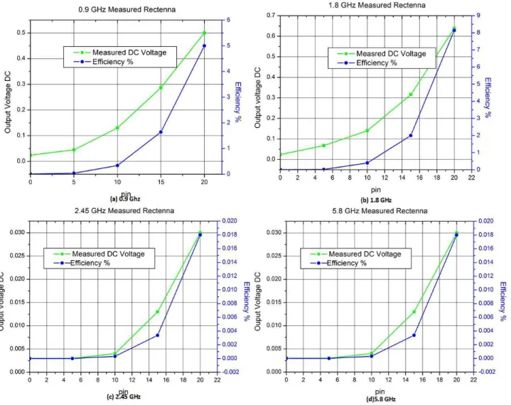
In this section, state-of-the-art literature review on various energy harvesting configurations is presented. Some of the presented work focuses on achieving high efficiency design, other focus on multiband energy harvesting while some focus on the compactness of the proposed rectenna designs.In [24], authors presented the design of a rectenna working at 2.45 GHz ISM band. The antenna was printed on FR4 substrate with thickness 1.6 mm using the simple microstrip patch design. The rectifier circuit was optimized using ADS simulator with its relevant capacitors and schottky diodes. The schottky diode used was from Avagos HSMS2860 series. As an experimental setup, horn antenna was used as an RF source to transmit power to the rectenna. Experimental results provided maximum output voltage of 50 mV at an input power of 10 dBm. Figure 2.8 and figure 2.9 show the fabricated prototype and DC output voltages of the rectenna.
Figure 2.7 Multiplier equivalent circuit [21].
19 | P a g e
Similarly in [25], authors proposed an ultra-compact low power rectenna working at 2.45 GHz but this time the technology used was paper based. The rectenna utilizes double layer technology where the antenna is on the back side with annular slot configuration while the remaining circuit components for the rectifier are on the other side of the substrate. The prototype was fabricated on a 230−μm thick paper sheet from Mitsubishi (ϵr = 2.55, tanδ = 0.05) by means of the copper tape technology, which consists of the shaping of an adhesive copper tape by standard photolithography and the application of the Cu pattern on the hosting substrate by means of a sacrificial layer. The schottky diode used was HSMS2850 series. For the experimental setup, a 4 dBi gain log periodic antenna was used. The rectenna was placed at a distance of 20 cm from the source. The measured results showed that the rectenna achieved an efficiency of 40 % around −10 dBm, of 28 % around −15 dBm, and in the range 10 % around −20 dBm, corresponding to an output DC voltage in the order of 320, 240 and 60 mV respectively.
Figure 2.9 DC Output voltage produces from the rectenna [24].
Figure 2.10 (a) Paper based annular slot antenna (b) rectifier on the back side of the paper [25].
20 | P a g e
A highly efficient UHF rectenna was presented in [26]. Authors implemented a novel idea with antenna design based on meander folded dipole technology having parasitic ground plane. The dimensions of the antenna was 41.3 mm x 17.5 mm at 915 MHz on a FR-4 based substrate. The rectifier circuit was based on a 5 stage charge pump having Cockroft-Walton voltage multipliers [17]. The conversion efficiency of the rectifier was 0.005% at a distance of 1.5 m realized on a FR4 board. Schottky diode, HSMS 285x and 286x, were used for its unique characteristics of very low signal compatibility feature (Pin <−20dB), and very low leakage current loss. A 3 V Zener diode was used to make it a ripple free DC voltage at 3 V and finally the output was measured across a 1.8 V distance. An UHF transmitter reader was to transmit microwave signals to the rectenna. The rectenna was able to harvest 200μW at an optimal distance of 1.5 m with the peak value of 647 μW at a distance of 0.5 m from the radiation source which was RFID based transmitter.
Figure 2.11 Rectenna measurement: output DC voltage (a) and RF-to-dc efficiency (b) versus available power at the input of the rectifier in the band 2.4-2.5 GHz [25].
21 | P a g e
Another antenna at UHF for mobile telephony bands was presented in [27]. The rectenna system was based on a broadband annular slot antenna and a thin flexible substrate, weighed fewer than 15 g. Thanks to the proper design of the rectifier and the matching network, an excellent performance was verified over the whole band (400 MHz – 1 GHz), with a rectenna conversion efficiency of up to 60% and an efficient figure of merit (EFoM) equal to 37.6 dB for 2 μW/cm2 of incident power density. The antenna was designed on Taconic TLY-5-0100 substrate (εr = 2.2,
tanδ=0.0009, and h=0.254 mm).
Figure 2.12 (a) Implemented antenna; (b) simulated and measured return loss; (c) implemented cockcroft-walton charge pump; (d) snapshot of the test bench to measure harvested power; (e) harvested
power vs distance curve [26].
22 | P a g e
In [28], authors proposed a dual band rectenna. This rectenna was working at the GSM bands (900/1800 MHz). Antenna was designed using meander lines on microstrip patch design which helped in reducing the size of the rectenna. Schottky diode SMS-7630 was used in the rectifier stage to convert the received signal into output voltage. Rectifier was optimized to receive signals as low as -20 dBm using harmonic rejection technique. The power conversion efficiency of 20% and 40.8% (in measurement) at the input power level of -20 dBm was achieved. The proposed rectenna had output voltage from 183-415 mV.
Similarly another dual band rectenna operating at 2.45 GHz and 5.8 GHz was presented in [29]. Square loop fed by a microstrip line technology was used to design the rectenna. Instead of exploiting multiband resonances from the square loop, for the first time according to the authors, half wavelength and full wavelength modes were generated from the design with the help of microstrip feed [29]. Impedance matching was achieved for the two resonances with the help of matching stub. The conversion efficiencies of 49% and 66% are achieved, respectively. The prototype rectenna measured only 13 mm × 24 mm or 0.106 λ0 × 0.196 λ0 at 2.45 GHz. Avago HSMS 2860 diode was used.
Figure 2.14: The rectified voltage at the rectenna output over frequency for three different power levels at the transmitter side, which correspond to power densities of 1.92, 0.61, and 0.19 μW/cm2, respectively [27].
23 | P a g e
Figure 2.16 Measured output voltage versus input power of only-rectifier and rectenna [28].
Figure 2.17 Fabricated prototype of rectenna [29].
24 | P a g e
In [30], a dual circular polarized energy harvesting rectenna based on six bands weas presented. Since diode in the rectifier stage is a non-linear device, its matching to get resonance at multiband is a challenge as varying input power or load can change its input impedance. In order to solve this, authors in [30] proposed an improved matching technique. They first realized a broadband antenna (550-2.5 GHz) with circular polarization and compact size. Compactness was acheinved using annular slots and novel feeding techniques. Then this wideband antenna was matched to a multiband rectifier with loads ranging from 10 to 75 kΩ. The measured results showed that the maximum harvested dc power of the rectenna in typical outdoor and indoor environments were 26 and 8 μW, respectively; it can therefore be applied to a range of low-power wireless applications.
Figure 2.19 Antenna and rectifier [30].
Figure 2.20 Measured received power versus frequency and measured output voltage of the proposed rectenna in (a) outdoor ambient environment and (b) indoor ambient environment [30].
25 | P a g e
A broadband rectenna array was presented in [31] having a triangular monopole antenna design. The antenna covered the electromagnetic spectrum from 800 MHz to 2.6 GHz. The gain was greater than 3.5 dBi from 900 MHz to 2.6 GHz and a maximum realized gain of 8.6 dBi was achieved at 2 GHz. Efficiency of 76% and 29% is obtained for a resistive load of 560 Ω at 900 and 1800 MHz, respectively. A voltage of 6.95 V for a load of 4.3 kQ was obtained close to a cell phone making a call.
Similarly another ultra-broadband rectenna was proposed in [32]. This time solar technology was used with amorphous silicon as a substrate. A 0.6-W Si panel of 10 solar cells arranged in a series of five pairs of parallel connected cells was used with Vivaldi antennas cutted ion to the panel. The 400-nm-thick a-Si layer of each cell was 71×18 mm2 and separated from other cells by a 2-mm gap. Each cell had seven silver electrodes on the front contact. The electrodes are 0.5×16.5 mm2 and separated by 9.5 mm. Rear contacts, 19.9×146 mm2, provided parallel connections between cells and were isolated from adjacent contacts by a 0.1-mm gap. The low-cost flexible panels were manufactured for one of many different power configurations, and the layout enabled various antenna shapes. End edge contacts on the panel were made from tin-coated copper plate. The entire panel was encapsulated by flexible polyimide layer. The rectenna maintained a peak power at 4.25 V, which overcomed a need for lossy power management components. The wireless communications device yielded solar energy or function as a rectenna for dual-source energy harvesting. The solar Vivaldi performs with 0.5-2.8 dBi gain from 0.95-2.45 GHz, and in rectenna mode, it covered three bands for wireless energy scavenging.
Distance of Cell Phone from Rectenna (cm)
Output voltage with
4.3K load (V) received Power (mW) 5 6.95 11.2 10 5.58 7.2 20 4.64 5 30 3.07 2.2 40 1.76 0.7
Figure 2.21 Experimental setup to measure RF energy harvested from the cell phone using 2 element array
for a load of 4.3kΩ [31].
Table 2.1 2-element array with output voltage when placed at a certain distance from source [31].
26 | P a g e
In [33], authors proposed a rectenna for a battery less thermal sensor operating at 2.45 GHz ISM band. The antenna was fabricated using microstrip technology and HSMS 2860 series schottky diodes were used for rectification. More than 80% efficiency was experimentally achieved at medium and low power densities. The circuit contained a symmetric and dual-access RF-to-dc rectifier and 2 patch antennas. The temperature sensor performs measurements every 10 seconds and required 1 V voltage and 30 μJ energy per period. It operated from low power densities of only 0.4μW/cm2 (E = 1.22 V/m).
-20 dBm -15 dBm -10 dBm
Freq Voltage Voltage Voltage
0.95 1.25 V 3.25 V 5.35 V
1.87 1.22 V 2.92 V 4.78 V
2.45 0.51 V 1.27 V 2.06 V
Figure 2.22 Fabricated Solar panel Vivaldi antenna [32].
Table 2.2 Measured results for various input power levels [32].
27 | P a g e
Reference Topology η RF to DC Operating Level Operating
Frequency Dimensions [24]
Realized Microstrip Patch antenna, voltage doubler
12.6 % 50 mV @ 10 dBm 2.45 GHz 37.6 × 29.15
mm2 [25]
Realized Paper Based Annular slot antenna, Series Rectifier 40 % 28 % 10% 320 mV @ −10 dBm 240 mV @ −15 dBm 60 mV @ -20 dBm 2.45 GHz 49 × 54 × 0.23 mm3 [26]
Realized Meander Folded Dipole Design, Boost Converter 0.005 % 200μW @ 1.5 m distance 647μW @ 0.5 distance 915 MHz 41.3× 17.5 ×1.5 mm3 [27]
Realized Annular Slot Antenna, Multistage voltage doubler 60 % EFOM 37.6 dB for 2 μW/cm2 of incident power density 800 MHz 83× 103 × 0.254 mm3 [28]
Realized Meander Stubs, voltage doubler 20 % 40 % 183 mV @- 20 dBm 415 mV @- 20 dBm 900 / 1834 MHz 0.254 mm42× 38 × 3 [29]
Realized Antenna, voltage Slot Loop doubler
49 %
66 % N/A 2.4 / 5.8 GHz 13 × 24 mm
2
[30]
Realized Cockroft-walton Spiral Antenna, doubler
67 % 96 µW @ -15 dBm 550 MHz -
2.5 GHz 160 × 160 ×1.6 mm3 [31]
Realized Monopole array Triangular antenna, voltage doubler 76 % @ 900 MHz. 29 % @ 1800 MHz 6.95 V at 4.3KΩ Load in close vicinity 800 MHz – 2.6 GHz 158 × 57 mm2 [32]
Realized on Amorphous Si Vivaldi Antenna -20 to -10 dBm 1.25 V @ 0.97 GHz 1.22 V @ 18 GHz 0.151 @ 2.45 GHz 0.97 GHz, 1.8 GHz, 2.4 GHz 710 ×180 mm2 [33]
Realized Microstrip Patch Array, DC-DC boost conversion
80 % 0.3 V 2.45 GHz N/A
Figure 2.24 Batteryless temperature-sensor prototype [33].
28 | P a g e
**Published in Microwave and Optical Letters Technology, Vol 59, 11, pp 2816-2822, Nov 2017.
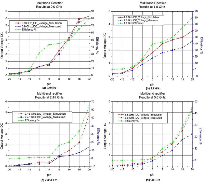
From the review that is presented in the above section, energy harvesting using RF source is still growing. Various design strategies and materials are being utilized in harvesting the maximum energies available in the atmosphere. Table 2.3 summarizes the state-of-the-art rectenna designs presented as literature review. It can be seen that most of the work is presented at 2.45 GHz, likely due to widespread usage. Limited work has been done in the multiband rectenna which shows more promise in terms of output voltage and efficiency. In the following sections, keeping with the harvesting spirit, a multiband antenna and a wideband rectifier is proposed. Both technologies are then combined and results are discussed in terms of efficiency and output DC voltage produced within a lab environment. The basic idea was to understand the working of the RF rectenna and present something to the research community as an alternate option for harvesting RF energy in the multiband spectrum.
2.4 Proposed Hexaband Antenna**
In this section, first part of the rectenna system, the receiving antenna is discussed. The proposed multiband antenna design is based on the monopole geometry which contains stubs or transmission lines of various lengths and widths. Using this technology will give us the required multi-bands that can be used for harvesting RF energy from various sources simultaneously. The details of the design and the results achieved are discussed in below sections.
2.4.1 Antenna Design
The geometry of the proposed hexaband antenna is shown in figure 2.25. The proposed antenna follows the principle of monopole antenna design where every printed monopole or stub length is
λ/4 according to its relevant frequency. The antenna is fabricated on RT Duroid 5880 substrate
with thickness of 1.57 mm, dielectric constant εr = 2.2 and loss tangent of 0.0009. The antenna is fed via a 50 Ω microstrip transmission line having a width and length of Wf x Lf = 2.8 mm x 87 mm. The overall antenna dimensions are Ws x Ls = 85 mm x 125 mm. The other side of the substrate has a finite ground plane with dimensions Wg x Lg = 54 mm x 60 mm and a rectangular slot with dimensions Wslot x Lslot = 0.7 mm x 7.6 mm. Each monopole antenna has been designed keeping in view its relevant frequency of operation. The capacitive coupling and parasitic looping of antenna elements also assists in achieving the required frequency resonance. The basic design consists of three monopole antennas with stubs introduced into the final design to achieve good bandwidth and resonances at bands of interest. Each monopole antenna element generates different resonant modes. The initial monopole, being the longest in length (Lf + L6), was designed to resonate at 900 MHz. The first monopole was loaded with a U-shaped stub to increase its electrical size, while maintaining its physical size and having a good resonance below -10 dB in terms of its reflection coefficient. The length of the inverted U-shaped stubs are L7 and L8 respectively with width represented by W2. The second resonance was achieved at 1800 MHz band by a monopole placed in the center of the feed line having a form of inverted L-shape with dimensions L2 and L3. The third resonance (the smallest in dimensions) is at 2.45 GHz. The stub was placed below the inverted L-shape with dimensions L1 and W1. The final and fourth resonance was achieved at the higher frequency of interest at 5.8 GHz by introducing a slot within the finite ground plane on the backside of the substrate. In order to investigate the role of each monopole resonating at a specific
29 | P a g e
frequency band and its effect on overall antenna performance, extensive parametric studies have been carried out and best optimized values for the hexaband antenna are tabulated in Table 2.4.
(a) (b)
Figure 2.25 Geometry of the proposed Hexaband Antenna (a) Front view (b) Back View.
2.4.2 Antenna Simulation and Experimental Results
Proposed hexaband antenna simulations were carried out using a commercial electromagnetic time domain finite integration technique (FIT) simulator known as Computer Simulation Technology Microwave Studio CST MWS [34]. Antenna characteristics such as return loss, radiation pattern and gain were calculated. The simulated antenna was realized using LPKF Protomat S100 machine and the fabricated prototype is shown in figure 2.26. The measurements of the prototype were done using Agilent PNA-X Network analyzer (N5245A). Simulated and measured return loss |S11| of the optimized antenna is shown in figure 2.27. The resonances at the required bands are well matched and useable for applications listed in Table 2.5, while the minor difference observed between the two results are due to fabrication losses and substrate permittivity tolerances.
To understand the working part of each monopole on antenna performance, the surface current distributions at the specific frequencies of interest i.e. 900 MHz, 1.8 GHz, 2.45 GHz and 5.8 GHz are shown in figure 2.28. It is observed that the longest monopole radiates for the lowest frequency of interest while the slot in the ground plane is responsible for resonance at the highest frequency. The 3D simulated radiation patterns of the proposed hexaband antenna are shown in
Parameter L1 L2 L3 L4 L5
Value 8 30 11.5 10.6 20
L6 L7 L8 W1 W2
24.6 80 15 2.8 4 Table 2.4 Optimized hexaband antenna parameters (MM).
30 | P a g e
figure 2.29, while the measured radiation polar plots of both the E-field and H-field components are shown in figure 2.30 for the above mentioned frequencies of interest. The maximum measured gain achieved at the 900 MHz, 1.8 GHz, 2.45 GHz and 5.8 GHz are 1.83 dB, 3.17 dB, 3.23 dB and 5.82 dB respectively. The radiation patterns reveal the antenna to be an omni-directional or donut shaped at the lower frequency bands i.e. GSM band however as the frequency tends to increase the gain also increases, hence becoming more directional for the higher frequency bands i.e. WLAN.
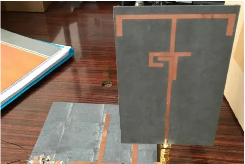
Figure 2.26 Photograph of fabricated hexaband antenna.
Figure 2.27 Measured and Simulated |S11| of the proposed hexaband antenna.
0.5 1 1.5 2 2.5 3 3.5 4 4.5 5 5.5 6 6.5 7 -30 -25 -20 -15 -10 -5 0 5 10 X: 6.391 Y: -10.18 Freq GHz Retu rn L oss dB S11 X: 5.35 Y: -9.811 X: 2.805 Y: -9.972 X: 2.293 Y: -10.22 X: 1.938 Y: -10.23 X: 1.729 Y: -10.59 X: 0.9163 Y: -10.4 X: 1.017 Y: -10.31 Measured S-parameters Simulated S-parameters Simulated Gain Measured Gain Gain
31 | P a g e
Figure 2.28 Surface current distributions for the proposed hexaband antenna.
32 | P a g e
33 | P a g e
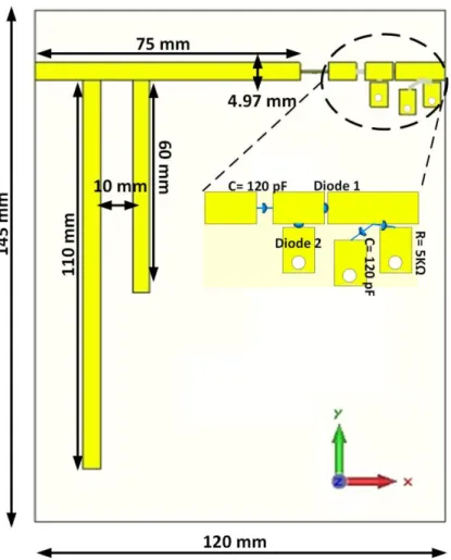
2.5 Proposed Multiband Rectifier
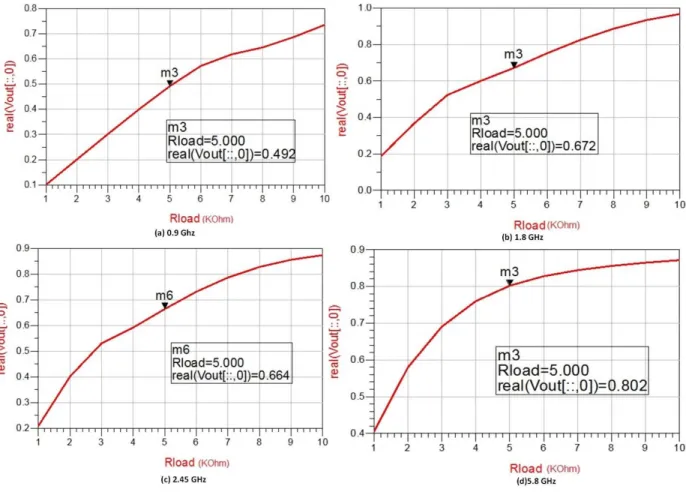
In this section a multiband rectifier is presented. The selection of the multiband rectifier is such that it complements the earlier presented hexaband antenna. Rectifier circuit is one of the main components in the energy harvesting rectenna system that converts the available energy into useable output DC voltage. A rectifier must be sensitive to power detection, have good power handling capabilities and consumes low operational power [35]. A conventional single series diode rectifying circuit is shown in figure 2.31 (a). It consists of an impedance matching network for transferring maximum power from the antenna to diode, a rectifying element (schottky diode) to achieve RF-to-DC conversion, a DC filter for smoothing the output DC voltage followed by a load resistor. The antenna receives the RF power which gets attenuated while passing through the impedance matching circuit and the schottky diode. The remaining power is converted into the dc power. The capacitor CL works as an energy storing device and also acting as a high-pass filter. The single series configuration of figure 2.31 (a) allows only the positive half cycle of the signal to get rectified while the negative half cycle is rejected by the diode. This configuration is not an efficient one because the ambient RF energy received on the antenna has very low power that is not enough to meet the biasing requirements of the schottky diode in order to initiate the rectifying process of the circuit. In addition, the breakdown voltage of the single diode rectifier is limited, which could affect the power handling capability of the circuit. An improved version, which was selected for the presented rectenna design, is called the Cockroft-Walton voltage doubler or Grainacher single stage doubler [36]. Figure 2.31 (b) shows the proposed voltage doubler design. The circuit receives the signal from the antenna, after passing through the matching network with appropriate attenuation. Diode D1 receives the positive half of the signal and stores in capacitor C1 while the negative half of the signal gets rectified by diode D2 with storage happening in capacitor C2. To get maximum or twice the output voltage, the energy stored in capacitor C2 can be transferred to capacitor C1 thus generating twice the output voltage across capacitor C1 at the load with a series configuration. This increases the breakdown voltage of the rectifier; hence the theoretical maximum conversion efficiency of the rectifier is also improved.
Frequency (MHz) Wireless Applications 870 – 900 GSM 850 (824-894 MHz) 900-1000 GSM 900 (880-960 MHz) 1722 – 1880 DCS (1710-1880 MHz) 1850-1900 PCS (1850-1900 MHz) 2287 - 2837 WLAN (2400-2480 MHz) 5713 – 6386 WLAN (5470-5725 MHz) Table 2.5 Frequency bands supported by hexaband antenna.
34 | P a g e
2.5.1 Schottky Diode Selection
In a rectifier circuit, the selection of the diode determines the overall performance of the circuit which leads to a better RF-to DC conversion efficiency. A zero biased schottky diode is normally used for rectifier designs that provides better sensitivity at low input power levels (-50 dBm to 0 dBm). Different kinds of schottky diodes have been proposed in literature [36-38] with their efficient rectifier circuit designs but the one that was suited to this research work for multiband resonance was purchased from Avago’s HSMS 2860 series schottky diode [39]. This dide belongs to the family of DC biased detector diodes designed to operate well in the frequency range of 915 MHz to 5.8 GHz. The applications it can support vary from RFID tag applications, signal modulation and demodulation, RF to DC conversion and voltage multiplication. The diode comes in various sizes and packages as per need of the application in terms of cost effectiveness and durability. Agilent’s manufacturing techniques assure the highest degree of match between two or more diodes when mounted on a surface package. The three important parameters that determine the power conversion efficiency of the diode are: breakdown voltage (Vbr), which limits the power handling capability of the rectifier circuit, the series resistance (Rs), which limits the efficiency; and zero-bias junction capacitance (Cj0), that affects how harmonic currents oscillate through the diode. Considering these specifications, our selected schottky diode HSMS 286B had the values of Rs =6 Ω, low value of Cj0 = 0.18 pF and Vbr = 7 V and a forward biasing voltage of Vf = 250 mV. This diode also has fast switching characteristics necessary for high frequency input signals and a low-cutoff voltage to operate at a low RF input power.
(a)
(b)
Figure 2.31 Rectifier circuit configurations : (a) Conventional Single Series setting, (b) Voltage Doubler setting.

![Figure 2.16 Measured output voltage versus input power of only-rectifier and rectenna [28]](https://thumb-eu.123doks.com/thumbv2/123doknet/7774111.257396/28.918.177.810.107.378/figure-measured-output-voltage-versus-input-rectifier-rectenna.webp)