This is an author-deposited version published in:
http://oatao.univ-toulouse.fr/
Eprints ID: 10192
To link to this article: DOI: 10.1109/TNS.2013.2249094
URL:
http://dx.doi.org/10.1109/TNS.2013.2249094
To cite this version:
Gaillardin, Marc and Goiffon, Vincent and Marcandella,
Claude and Girard, Sylvain and Martinez, Martial and Paillet, Philippe and
Magnan, Pierre and Estribeau, Magali Radiation Effects in CMOS Isolation
Oxides: Differences and Similarities With Thermal Oxides. (2013) IEEE
Transactions on Nuclear Science, vol. 60 (n° 4). pp. 2623-2629. ISSN
0018-9499
Open Archive Toulouse Archive Ouverte (OATAO)
OATAO is an open access repository that collects the work of Toulouse researchers and
makes it freely available over the web where possible.
Any correspondence concerning this service should be sent to the repository
administrator:
[email protected]
Radiation Effects in CMOS Isolation Oxides:
Differences and Similarities with Thermal Oxides
M. Gaillardin, Member IEEE, V. Goiffon, Member IEEE, C. Marcandella, S. Girard, Senior Member
IEEE, M. Martinez, P. Paillet, Senior Member IEEE, P. Magnan, Member IEEE, M. Estribeau, Member
IEEE
1Abstract – Radiation effects in thick isolation oxides of
modern CMOS technologies are investigated using
dedicated test structures designed using two
commercial foundries. Shallow Trench Isolation and Pre-Metal Dielectric are studied using electrical measurements performed after X-ray irradiations and isochronal annealing cycles. This paper shows that trapping properties of such isolation oxides can strongly differ from those of traditional thermal oxides usually used to process the gate oxide of Metal Oxide Semiconductor Field Effect Transistors. Buildup and annealing of both radiation-induced oxide-trap charge and radiation-induced interface traps are discussed as a function of the oxide type, foundry and bias condition during irradiation. Radiation-induced interface traps in such isolation oxides are shown to anneal below 100°C contrary to what is usually observed in thermal oxides. Implications for design hardening and radiation tests of CMOS Integrated Circuits are discussed.
Keywords – Total Ionizing Dose (TID), CMOS, Shallow
Trench Isolation (STI), Pre-Metal Dielectric (PMD), transistors, CMOS image sensors (CIS).
I. INTRODUCTION
The generation of charges by ionizing radiations in CMOS materials may induce stable defects in dielectrics [1] used in the fabrication process. This phenomenon results in modifications of CMOS devices electrical characteristics, such as threshold voltage shifts in MOSFETs, or intense leakage currents. Since the number of defects generated in gate-oxide reduces with its thickness, this effect becomes negligible in modern Integrated Circuits (ICs). Total Ionizing Dose (TID) induced degradation of modern CMOS integrated circuits is thus now governed by field or isolation oxides such as Shallow Trench Isolation (STI) [2,3] or Pre-Metal Dielectric (PMD). They are deposited oxides contrary to the widely studied gate-oxide which is thermally grown. Unlike thermally grown oxides, few data are available on trapping properties and interface trap buildup rate of these deposited oxides456789[4-9]. Most studies on deposited oxides focus on electrical effects in ICs due to trapping in STIs 10111213[10-13]. A complete analysis of physical mechanisms occurring in deposited oxides - STI but also PMD [14] - under ionizing radiation and after
M. Gaillardin, C. Marcandella, M. Martinez, and P. Paillet are with CEA, DAM, DIF, F-91297 Arpajon, France.
S. Girard is with Laboratoire H. Curien, UMR CNRS 5516, Université Jean Monnet, 18 rue du Pr. Benois Lauras, 42000, Saint-Etienne, France.
V. Goiffon, P. Magnan and M. Estribeau are with ISAE, Université de Toulouse, 10 avenue Edouard Belin, BP 54032, 31055 Toulouse Cedex 4, France.
annealing remains needed. This will help foreseeing the behavior of future technologies designed for specific applications which are very sensitive to deposited oxide such as analog devices, bipolar technologies [15,16], DRAMs, or CMOS image sensors 171819[17-19]. In this paper, we investigate the defect density evolution of two types of thick deposited oxides submitted to Total Ionizing Dose (TID) using dedicated custom test structures processed in two deep submicron commercially available technologies. This paper is especially focused on the ionizing radiation behavior of grounded deposited oxides which play an important role in the radiation response of several CMOS ICs. For instance, in CMOS Image Sensors (CIS) the most sensitive node is the photodiode which is surrounded by a grounded deposited oxide (STI or PMD). However, it may also be critical in circuits where the leakage current of any PN junction in a CMOS ICs is an issue. So, knowing the behavior of thick isolation oxides grounded during irradiation will help one to improve hardening level of CMOS ICs.
II. EXPERIMENTAL DETAILS A. Test structures
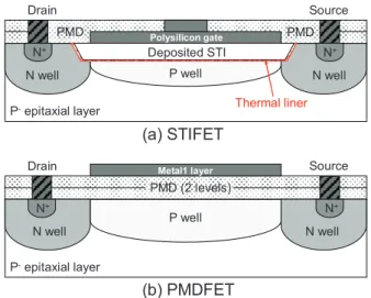
Specific devices were fabricated using two commercial bulk 0.18 µm processes. They consist in large NMOS transistors which gate oxide is made of either a STI (Fig. 1.a) or a PMD (Fig. 1.b), both being deposited oxides. In the following, they are referred to as STIFET and PMDFET respectively. In both devices the Pwell-doped region is located under the thick “gate oxide” and between two Nwell-doped regions which act as source and drain. The gate is either made of standard polysilicon or of the first metal layer from the back end of line. The exact details of the process are not described in this paper. However, usual STI process flows involve a thin thermally grown liner followed by the STI deposition before planarization. The thermal liner is about 30 nm thick and the total STI stack thickness is about 400 nm [20]. The PMD follows several process steps after the STI creation: gate oxide growth, gate polysilicon deposition, gate lithography and Reactive Ion Etching (RIE) of the entire wafer before PMD deposition [20]. This way, the gate oxide is removed on the entire wafer, except under the gate electrode. There is no “high quality” oxide between the PMD, usually deposited in two steps, and the active silicon. The complete PMD-stack is about 550 nm-thick. Since we do not have the process details, it is hard to know whether or not a liner remains between the active silicon and the PMD. Figure 1 thus presents only schematic configuration of the designed custom test structures as accurately as possible. One should notice that the PMDFET has been designed only using one process. For
the experiments, devices are mounted in standard dual in-line packages. Variability issues are not discussed in the scope of this paper since only few test structures have been tested for this study.
B. Experiments
Each test structure is irradiated at room temperature using 10-keV X-rays. The dose rate is fixed at a constant value of 100 rad(SiO2)/s. The total dose is deposited in several
irradiation steps to reach 100 krad(SiO2) at maximum.
PMD Polysilicon gate PMD N well N well Drain Source P well PMD (2 levels) Metal1 layer N well N well Drain Source P well (a) STIFET (b) PMDFET P-epitaxial layer P-epitaxial layer Thermal liner Deposited STI N+ N+ N+ N+
Figure 1: Schematic configuration of (a) the STIFET and (b) the PMDFET.
Each total dose irradiation step is immediately followed by static electrical measurements performed using a HP 4145 parametric analyzer. Only the gate terminal can be biased during the irradiation experiments, in order to apply a constant electric field across the oxide between the gate electrode and the silicon/oxide interface. All other electrodes (source, drain, pwell and substrate) are grounded. The gate is either grounded or biased to the nominal voltage of the technology to study the electric field dependence of the charge trapping properties of thick oxides under irradiation and get the worst irradiation configuration. The bias applied to the PMDFET gate is chosen to get the same electric field across the PMD than in the STI despite their different thicknesses.
After the last x-ray irradiation, isochronal annealing experiments are performed to get insights on the fraction of charges that remain trapped in the oxide as a function of temperature. Temperature increases from room temperature to reach 250°C by steps of 25°C. The step duration is fixed at 30 min as proposed in [21]. Devices are grounded during each annealing step. I-V measurements are then performed after a short cooling obtained by injecting a gaz mixture involving nitrogen in our specific setup dedicated to annealing experiments to reach rapidly the room temperature after each 30 min temperature stress. Devices are always grounded during anneals.
III. RESULTS AND DISCUSSION
A. Ionizing radiation effects in grounded isolation oxides The PMDFET TID response is characterized in figure 2. The device is grounded during irradiation. Electrical characteristics exhibit a large negative voltage shift due to radiation-induced positive charge trapping in the gate
oxide manufactured with a Pre-Metal Dielectric. Figure 2 also highlights that the subthreshold slope does not significantly change with TID. This means that the interface traps formation is limited when the device is grounded during irradiation.
-20 -10 0 10 20 30 40 50 60 70 80 10-14 10-13 10-12 10-11 10-10 10-9 10-8 10-7 10-6 10-5 10-4 10-3 10-2 10-1 Before irradiation PMDFET - process A
Unbiased during irradiation
100 krad(SiO2) D ra in c u rr e n t ID ( A ) Gate voltage VGS (V)
Figure 2: Drain current vs gate voltage characteristics of the PMDFET from process A at several total dose steps from before irradiation (black squares) to 100 krad(SiO2) (red circles). Irradiation steps include pre-rad,
10 k, 20 k, 30 k, 50 k, 70 k and 100 krad. Device was biased at 0V during irradiation.
STIFETs electrical characteristics from process A and B are displayed in figure 3 for the exact same irradiation conditions and they strongly differ. The subthreshold slope is degraded in both STIFET characteristics revealing an interface trap buildup in addition to the positive charge trapping in the oxide. This is especially true for the STIFET from foundry B (Figure 3, bottom) for which the subthreshold slope is visually degraded. So, not only is the TID response of PMD different from the one of STI, but also the TID response of STI fabricated using two different processes. 10-13 10-12 10-11 10-10 10-9 10-8 10-7 10-6 10-5 10-4 10-3 10-2 10-1 Before irradiation STIFET - Process A
Unbiased during irradiation
100 krad(SiO2) D ra in c u rr e n t ID ( A ) -20 -10 0 10 20 30 40 50 60 70 80 10-14 10-13 10-12 10-11 10-10 10-9 10-8 10-7 10-6 10-5 10-4 10-3 10-2 Before irradiation STIFET - Process B
Unbiased during irradiation
100 krad(SiO 2) D ra in c u rr e n t ID ( A ) Gate voltage VGS (V)
Figure 3: Drain current vs gate voltage characteristics of STIFETs from two commercial foundries at several total dose steps from before irradiation (black squares) to 100 krad(SiO2) (red circles). Irradiation
steps include pre-rad, 10 k, 20 k, 30 k, 50 k, 70 k and 100 krad. Devices were unbiased during irradiation.
In the following, the charge separation technique [22] is used to estimate the contribution related to oxide-trapped charges Vot compared to the one due to interface traps
VIT. Parameter variations are presented as a function of
TID in figure 4. 0 20 40 60 80 100 -20 -15 -10 -5 0 5 10 15 20 : STIFET - Process A : STIFET - Process B : PMDFET - Process A ∆VOT ∆ VIT , ∆ VO T ( V )
Total Ionizing Dose (krad(SiO2))
∆VIT
Figure 4: Voltage shifts vs Total Ionizing Dose associated to oxide-trap charge VOT and to interface traps VIT for PMDFET (red circles) and
STIFETs (black squares). Devices are grounded during irradiation. Voltage shifts are extracted for devices grounded during irradiation for each device. Figure 4 confirms previous observations regarding figures 2 and 3. All oxides exhibit clear evidence of an oxide-trap charge buildup with TID as already observed in several thermal oxides [8]. They all show a large contribution of VOT, differences in absolute
values being due to deposition process parameters such as temperature, pressure and process type.
On the other hand, the role of interface traps clearly differs from a deposited oxide to the other. Their contribution stays within measurement uncertainties for the PMDFET. An explanation may be that its gate is made of metal instead of polysilicon in the case of STIFET. The use of a metal gate processed with post-metal anneals in a variety of ambients has already shown that midgap interface trap density can be strongly reduced [23]. Moreover, variations in gate workfunctions (metal or polysilicon) and doping concentrations in the silicon may lead to slight electric field differences through the oxide. Hole transport in the PMDFET may thus be reduced, limiting interface traps formation at the PMD/silicon interface.
Despite a “close-to-zero” electric field, even with a polysilicon gate, both STIFETs show large VIT. Interface
trap contribution in STIFET from process B (figure 4, open squares) reaches 15 V after 100 krad(SiO2) which is
equivalent to the one of oxide-trap charge.
In the STI process, a thermal oxide liner is grown before the STI deposition. This first liner is highly passivated with hydrogen. It may easily be depassivated under irradiation inducing the interface trap formation depicted in Figure 4. By contrast, the PMD is deposited without high quality dielectric liner as stated in II.A. The PMD/silicon interface is not passivated during the fabrication process and can thus not be depassivated under irradiation leading to strongly limited interface traps buildup. The TID response of deposited oxides used in modern CMOS technologies behave in a different manner than traditional thermal oxides. The process used to
fabricate dielectrics (including liner layers in the case of STI), various annealing temperatures and doping appear to be key aspects in determining the trapping properties of such oxides.
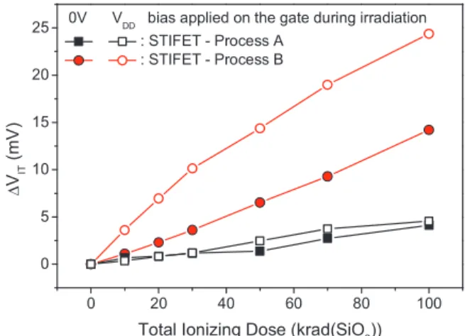
B. Effect of biasing on TID response of isolation oxides Voltage shifts due to oxide-trap charges and to interface traps are now displayed in Figure 5 and Figure 6. Parameter extractions from measurements obtained on gate-biased STIFETs from processes A and B are presented to discuss the effect of the electric field and to get the worst irradiation case.
0 20 40 60 80 100 -40 -35 -30 -25 -20 -15 -10 -5 0 5 VG = 3.3 V during irrad. : STIFET - Process A : STIFET - Process B ∆ VO T ( m V )
Total Ionizing Dose (krad(SiO2)) VG = 0 V during irrad.
Figure 5: Voltage shifts vs Total Ionizing Dose associated to oxide-trap charge VOT for STIFET from process A (black squares) and process B
(red circles). Devices are either grounded (filled symbols) or gate-biased (open symbols) during irradiation.
As intended, greater voltage shifts are achieved when devices are biased under irradiation in both processes. Biasing the gate with a positive bias induces electric field lines that start from the gate to reach the STI/active silicon interface. This enhances the separation of radiation generated electron-hole pairs and the transport of carriers escaping initial recombination in this area. Most oxide trapped charges are thus trapped close to the STI/silicon interface inducing a stronger voltage shift than when devices are grounded during irradiation.
0 20 40 60 80 100 0 5 10 15 20 25 : STIFET - Process A : STIFET - Process B ∆ VIT ( m V )
Total Ionizing Dose (krad(SiO2)) 0V VDD bias applied on the gate during irradiation
Figure 6: Voltage shifts vs Total Ionizing Dose associated to interface traps VIT for STIFET from process A (black squares) and process B (red
circles). Devices are either grounded (filled symbols) or gate-biased (open symbols) during irradiation.
The interface traps generation was also demonstrated to be a bias dependent mechanism [24,25] since it is mainly driven by the drift of hydrogen ions through the oxide/silicon interface [1,26]. However, Figure 6 shows clear discrepancies between the radiation response of the STIFET from process A (black squares) and process B (red circles).
First, measurements presented in Figure 6 show that the buildup of interface traps remains limited in the STIFET fabricated using process A either grounded (filled black squares) or gate-biased (open black squares) during irradiation. The voltage shift due to interface traps reaches 4.56 V for gate-biased devices during irradiation and 4.11 V for grounded devices. The voltage shift due to interface traps is thus only enhanced by about 10 % when devices are gate-biased. This means that the bias applied to the gate does not play an important role in the radiation induced interface traps buildup at the STI/silicon interface of devices from process A.
By contrast, measurements performed on STIFETs from process B (Figure 6, red circles) exhibit larger contributions of the interface traps VIT than in STIFETs
from process A, gate-biased (open red circles) or not (filled red circles) during irradiation. Results show a strong bias dependence of the interface traps buildup compared to what is observed on the STIFET from process A despite the same electric field applied across the STI in both cases. VIT reaches 14.2 V for devices grounded during
irradiation and more than 24 V for gate-biased devices during irradiation. This value is about five times higher than in STIFET from process A. Possible causes to explain these differences may be found in the STI stack composition. The liner, the nature and doping of the deposited oxide and the associated fabrication processes with their related thermal budgets each play an important role in the observed radiation responses. In process B, the STI/silicon interface seems easily depassivated by hydrogen ions which drift rapidly across the deposited oxide. Moreover, the liner between the active silicon and the deposited STI may be of a lower quality than the one fabricated using the process A.
C. Contribution of oxide-trap charges
Isochronal annealing is a convenient tool to separate contribution of trapped charges from the one related to interface traps. It is well established that in most cases, temperatures as high as 100°C are sufficient to enhance the annealing rate of trapped charges in thermally grown gate-oxides, while it is not the case for interface traps [1]. Usually, after the typical one week annealing at 100°C used for space qualification, the radiation induced trapped positive charge disappears whereas the interface trap density reaches its maximum value.
Figure 7 presents results of isochronal annealing performed on STIFETs from processes A and B irradiated at 100 krad(SiO2). Devices are grounded during anneals.
Figure 7 displays the oxide-trap charge neutralization with increasing temperature. Two different kinetics of recovery are exhibited. 0 50 100 150 200 250 0.0 0.1 0.2 0.3 0.4 0.5 0.6 0.7 0.8 0.9 1.0 Process B NO T u n a n n e a le d f ra c ti o n Annealing Temperature (°C) STIFETs Process A
Figure 7: Evolution of oxide trapped charge density during isochronal annealing experiments (30 min isochronal annealing step duration).
STI from process A exhibits a smooth monotonic decrease which begins at 100°C (black squares). 40 % of radiation-induced charges remain trapped in the oxide after 250°C annealing. Here, neutralization of oxide-trap charge varies only with temperature since devices are grounded during anneals. Thermal emission of electrons from the valence band [8] into a trap should thus be the dominant mechanism to explain the anneal process. Tunneling of electrons from silicon should not occur since this mechanism depends on the electric field and not on the temperature. So, increasing temperature allows neutralization of deeper traps in the oxide band gap. The smooth shape exhibited in figure 7 for the STI from process A suggests that the energy distribution of oxide traps is relatively spread out over the STI band gap. STI from process B behaves in a different way (figure 7, red circles). The shape reveal several steps at 50°C and 150°C suggesting that the energy distribution of traps is not as continuously spread as in process A. Two or more energy levels that correspond to temperature steps exhibited in Figure 7 may be inferred from these data. The first one is neutralized at low temperature (between 25°C to 75°C) and should be very close to the oxide valence band. Other trap energy levels are located deeper in the oxide band gap since higher temperatures (100°C and 150°C) are needed to anneal the related trapped charges. It must be noted that oxide trapped charge anneals at lower temperature than in the STI of Process A. This means that energy levels of traps are localized closer to the valence band than in the STI from Process A since a lower energy, i.e. temperature, is needed to neutralize the trapped charges. This characteristic highlights the different oxide nature between two STI processes of the same technology node but from two different foundries.
D. Contribution of interface traps
The same approach is now used to study the annealing characteristics of interface traps. In our N-type samples, interface traps located in the upper portion of the silicon bandgap are predominantly acceptors and thus negatively charged.
It is commonly assumed in thermal oxides that interface traps do not anneal at room temperature and that the rate of interface traps buildup increases with temperature [8] (up to 125°C). Figure 8 clearly shows on devices from two foundries that interface traps anneal even for temperature ranges below 100°C contrary to what was expected in thermal oxides [27, 28].
Some examples of interface traps annealing in thermal oxides were already described in the literature293031[1, 29-31]
but higher temperatures (more than 150°C) are normally required to observe significant interface trap annealing [21]. Fleetwood et al. [32] have shown such annealing with devices biased at 0 V, as already observed here. Furthermore, the post-irradiation recovery of bipolar transistors observed in [33] was also attributed to the annealing of interface traps. Results presented in [33] suggested that “it would appear that significantly more interface traps would appear in the base oxide of the lateral/substrate PNP input transistor would have to be annealed at 100°C, compared to what has typically been observed in high quality thermal oxide”. One explanation raised by the authors was that the thick oxide involved in this behavior is a deposited oxide and thus the annealing properties of such oxide could strongly differ from that of thermal oxides. This is clearly what is pointed out by annealing results presented in Figure 8 which were obtained on test structures dedicated to the study of such deposited oxides fabricated using two different sub-micron commercial CMOS processes. Here, both deposited oxides exhibit a minimum of 50 % recovery at 100°C, and less than 30 % of interface trap density remains after 125°C. This means that electrical characteristics almost retrieve their initial shape after the 125°C isochronal annealing as it is presented in I-V characteristics of Figure 9 on the STIFET of process B. 0 50 100 150 200 250 0.0 0.2 0.4 0.6 0.8 1.0 Process B NIT u n a n n e a le d f ra c ti o n Annealing Temperature (°C) STIFETs Process A
Figure 8: Evolution of interface trap density during isochronal annealing experiments (30 min isochronal annealing step duration).
After 250°C (black squares), interface traps are entirely annealed. The subthreshold slope then retrieves its initial value. Only the threshold voltage remains negatively shifted of few volts from its original value because of the 25 % unannealed fraction of oxide-trap charge, as depicted in Figure 7 after 250°C.
These results confirm the few results already published on the annealing behavior of radiation induced interface traps in STI [10,13,14]. It clearly shows that the conclusion
drawn on the behavior of thermal oxides during thermal annealing can not directly be transposed to the annealing behavior analysis of modern CMOS ICs.
The mechanism of annealing of interface traps is still a matter of debate like the one for their formation. The release and transport of hydrogen ions is in most cases pointed out [6] to explain the interface trap buildup by breaking Si-O or Si-OH bonds at the Si/oxide interface. However, interface trap annealing observed up to 250°C may also be due to hydrogen which moves toward the interface to re-passivate the radiation-induced interface traps. At this point, the mechanism for interface trap annealing is still an open question.
E. Potential implications and design hardening
For both oxides, the reported results may have potential implications for device hardening and hardness assurance for a wide range of electronic applications. In addition to the well know importance of STI in the radiation hardness of modern CMOS ICs, one can note many particular cases where PMD can be the main weakness when exposed to ionizing radiation like in CIS. Performances of CMOS ICs which radiation hardness can be limited by junction leakages (e.g. dark current in image sensors, retention time in DRAMs…) are most of time dependent on the behavior of isolation oxides and especially interface trap densities at STI interfaces. The reported results can help understanding the behavior of such devices in ionizing environment and can thus help improving the testing guidelines and mitigation techniques. -20 -10 0 10 20 30 40 50 60 70 80 10-14 10-13 10-12 10-11 10-10 10-9 10-8 10-7 10-6 10-5 10-4 10-3 10-2 10-1 : 25°C : 125°C : 250°C
STIFET - Process B after irradiation
Grounded during annealing
D ra in c u rr e n t ID ( A ) Gate voltage VGS (V) Pre-rad
Figure 9: Drain current vs gate voltage characteristics of STIFET fabricated using process B irradiated at 100 krad(SiO2) after several steps
of isochronal annealing: 25°C (red circles), 125°C (blue triangles) and 250°C (black squares). Devices are grounded during annealing. The pre-irradiation characteristic is also displayed with dashed lines.
For example, knowing that interface traps anneal at low temperature can explain the good recovery usually reported for image sensors after a 100°C annealing [34,35,36] (whereas it would have been attributed to trapped charge annealing if the conclusions drawn on thermal oxides were directly transposed to analyze such devices). It was also suggested in [33] that the annealing of a significant amount of interface traps in the base oxide of the lateral/substrate PNP input transistor at 100 °C could explain the post-irradiation recovery of bipolar transistors for which the base oxide is made of a composite deposited dielectric. Our results agree with such hypothesis by demonstrating the low temperature annealing of interface
traps using measurements performed on dedicated test structures. Then, such effect has to be taken into account to correctly define guidelines for radiation test of such ICs. The unnoticeable interface trap buildup in PMDFET fabricated using the process A can be used to harden critical junctions (e.g. photodiodes in image sensors, sampling capacitance in analog ICs or storage node in DRAMs), simply by isolating these junctions by PMD instead of STI. However, this specific property of process A should be checked in other technologies since both PMDFET and STIFET from process A seem less prone to interface formation than devices from process B. Finally, it could also explain why recessing the STI has been shown to improve radiation hardness of CMOS photodiodes [37].
V. CONCLUSION
This paper investigates the degradation of thick isolation oxides used in modern CMOS fabrication processes. This study focuses on Pre-Metal Dielectric and on Shallow Trench Isolation processed using two commercial technologies. Behaviors of PMD and STI under ionizing radiation strongly differ showing large variations of oxide-trap and interface-oxide-trap buildup with or without electric field applied across the oxide.
Measurements performed on custom test structures evidence a strong fabrication process dependence of the radiation response of deposited oxides as already observed on thermal oxides [21]. Results pointed out that the two STI oxides behave in a strongly different way. The buildup of interface traps especially exhibit two various behaviors, one being clearly driven by the electric field through the oxide (process B) compared to the other (process A). STI fabricated using two commercial processes are then investigated using isochronal annealing experiments. Oxide-trap charge neutralization shows a clear temperature dependence which involves thermal emission of electrons. The two STI oxides also differ in their annealing characteristics. The first one shows a smooth recovery of oxide-trap charges whereas the second exhibits a step by step mechanism. This means that energy distributions of oxide traps are either widely spread over the band gap for process A or more precisely located through distinct energy levels in process B. Furthermore, these data suggest that trapping levels are more deeply located in the bandgap of the STI from process A than in process B. This last fabrication process involves trapping levels closer to the valence band making easier the detrapping of radiation induced charges in the STI. Finally, experiments confirm the large interface trap annealing in both deposited oxides even for temperatures below 100°C which is not usually seen in thermal oxides. Almost all interface traps are annealed at 250°C for both fabrication processes of such deposited oxides. These results can have direct implications on radiation test guidelines and mitigation techniques of modern CMOS ICs which are limited by the degradation of STI and PMD oxides, especially for those where interface traps are involved like CIS or bipolar transistors.
Additional irradiations and annealing experiments under various electric field conditions remain needed for future
work to discuss in more details which physical mechanisms are involved in the trapping/detrapping properties of isolation oxides fabricated using commercial CMOS processes.
REFERENCES
[1] T.P. Ma and P.V. Dressendorfer, Ionizing Radiation Effects in MOS
Devices and Circuits, New-York: Wiley-Interscience, 1989.
[2] M. Turowski, A. Raman, R. D. Schrimpf, “Nonuniform total-dose-Induced charge distribution in Shallow-Trench Isolation oxides”, IEEE T[rans. Nucl. Sci., vol. 51, n°6, p. 3166, 2004.
[3] M.R. Shaneyfelt, P.E. Dodd, B.L. Draper, R.S. Flores, “Challenges in hardening technologies using shallow trench isolations”, IEEE Trans. Nucl. Sci., vol. 45, n°6, p. 2584, 1998.
[4] V. Ferlet-Cavrois, T. Colladant, P. Paillet, J.L. Leray, O. Musseau, J.R. Schwank, M.R. Shaneyfelt, J.L. Pelloie, J. du Port de Pontcharra, “Worst case bias during total dose irradiation of SOI transistors”, IEEE Trans. Nucl. Sci., vol. 47, n°6, p. 2183, 2000.
[5] R.E. Stahlbush, G.J. Campisi, J.B. McKitterick, W.P. Maszara, P. Roitman, G.A. Brown, “Electron and hole trapping in irradiated SIMOX, ZMR and BESOI buried oxides”, IEEE Trans. Nucl. Sci., vol. NS-39, n°6, p. 2086, 1992.
[6] W.L. Warren, M.R. Shaneyfelt, J.R. Schwank, D.M. Fleetwood, P.S. Winokur, R.A.B. Devine, W.P. Maszara, J.B. McKitterick, “Paramagnetic defect centers in irradiated BESOI and SIMOX buried oxides”, IEEE Trans. Nucl. Sci., vol. NS-40, n°6, p. 1755, 1993. [7] B.J. Mrstik, H.L. Hughes, P.J. Marr, R.K. Lawrence, D.I. Ma, I.P. Isaacson, R.A. Walker, “Hole and electron trapping in ion implanted thermal oxides and SIMOX”, IEEE Trans. Nucl. Sci., vol. 47, n°6, p. 2189, 2001.
[8] J.R. Schwank, “Total dose effects in MOS devices”, NSREC Short Course, 2002.
[9] P. Paillet, J.L. Autran, J.L. Leray, B. Aspar, A.-J. Auberton-Hervé, “Trapping-detrapping properties of irradiated ultra-thin SIMOX buried oxides”, IEEE Trans. Nucl. Sci., vol. 42, n°6, p. 2108, 1995.
[10] F. Faccio, G. Cervelli, “Radiation-induced edge effects in deep submicron CMOS transistors”, IEEE Trans. Nucl. Sci, vol. 52, n°6, p. 2413, 2005.
[11] M. Gaillardin, V. Goiffon, S. Girard, M. Martinez, P. Magnan, P. Paillet, “Enhanced radiation induced narrow channel effects in a commercial 0.18 µm bulk technology”, IEEE Trans. Nucl. Sci, vol. 58, n°6, p. 2807, 2011.
[12] C. Brisset, V. Ferlet-Cavrois, O. Flament, O. Musseau, J.L. Leray, J.L. Pelloie, R. Escoffier, A. Michez, C. Cirba, G. Bordure, “Two-dimensional simulation of total dose effects on NMOSFET with lateral parasitic transistor”, IEEE Trans. Nucl. Sci, vol. 43, n°6, p. 2651, 1996. [13] F. Faccio, H.J. Barnaby, X.J. Chen, D.M. Fleetwood, L. Gonella, M. McLain, R.D. Schrimpf, “Total ionizing dose effects in shallow trench isolation oxides”, Microelectronics Reliability, 2008.
[14] V. Goiffon, C. Virmontois, P. Magnan, S. Girard, P. Paillet, “Analysis of Total Dose-Induced Dark Current in CMOS Image Sensors From Interface State and Trapped Charge Density Measurements“, IEEE Trans. Nucl. Sci., Vol. 57, n°6, p.3087, 2010.
[15] A.H. Johnston, G.M. Swift, B.G. Rax, “Total dose effects in conventional bipolar transistors and linear integrated circuits”, IEEE Trans. Nucl. Sci., vol. 41, n°6, p. 2427, 1994
[16] Z. Xiao, M. Qiao, B. Zhang, J. Xu, “Total dose characteristics of high voltage LDMOS on SIMOX substrate”, Proc. Of the International Conference on Communications, Circuits and Systems, p. 1265, 2007. [17] G.R. Hopkinson, “Radiation effects in a CMOS active pixel sensor”, IEEE Trans. Nucl. Sci, vol. 47, n°6, p. 2480, 2000.
[18] V. Goiffon, M. Estribeau, P. Magnan, “Overview of ionizing radiation effects in image sensors fabricated in a deep-submicrometer CMOS imaging technology”, IEEE Trans. Electron. Dev., vol. 56, n°11, p. 2594, 2009.
[19] C. Virmontois, V. Goiffon, P. Magnan, O. Saint-Pe, S. Girard, S. Petit, G. Rolland, A. Bardoux, “Total ionizing dose versus displacement damage dose induced dark current random telegraph signals in CMOS image sensors”, IEEE Trans. Nucl. Sci, vol. 58, n°6, p. 3085, 2011. [20]Y. Taur and T.H. Ning, “Fundamentals of Modern VLSI Devices”, second edition (reprinted), Cambridge University Press, 2010, appendix 1: ”CMOS Process Flow”.
[21]A. J. Lelis, T. R. Oldham, and W. M. DeLancey, “Response of Interface Traps during High-Temperature Anneals,” IEEE Trans. Nucl. Sci. vol. 38, no. 6, pp. 1590-1597, Dec. 1991.
[22] P.J. McWhorter, P.S. Winokur, “Simple technique for separating the effects of interface traps and trapped-oxide charge in metal-oxide-semiconductor transistors”, Appl. Phys. Lett., vol. 48, n°2, p. 133, 1986. [23] M. L. Reed, J. D. Plummer, “Chemistry of Si-Si02 Interface Trap Annealing”, J. Appl. Phys., Vol. 63, p. 5776, 1988.
[24] N. S. Saks, D. B. Brown, and R. W. Rendell, “Effects of Switched Bias on Radiation-Induced Interface Trap Formation,” IEEE Trans. Nucl. Sci. vol. 38, no. 6, pp. 1130-1139, 1991.
[25] P. S. Winokur, H. E. Boesch, Jr., J. M. McGarrity, and F. B. McLean, “Field- and Time-Dependent Radiation Effects at the Si/SiO2 Interface of Hardened MOS Capacitors,” IEEE Trans. Nucl. Sci. vol. 24, no. 6, pp. 2113-2118, Dec. 1977.
[26] J. M. McGarrity, P. S. Winokur, H. E. Boesch, Jr., and F. B. McLean, “Interface States Resulting from a Hole Flux Incident on the SiO2/Si Interface,” Physics of SiO2 and Its Interfaces, 1978, pp. 428-432. [27] P.L. McWhorter, W. Miller, “Modeling the anneal of radiation-induced trapped holes in varying thermal environment”, IEEE Trans. Nucl. Sci. Vol. 37, n°6, p. 1682, 1990.
[28] D. M. Fleetwood, F. V. Thome, S. S. Tsao, P. V. Dressendorfer, V. J. Dandini, and J. R. Schwank, “High-Temperature Silicon-On-Insulator Electronics for Space Nuclear Power Systems: Requirements and Feasibility,” IEEE Trans. Nucl. Sci. vol. 35, no. 5, 1099-1112, Oct. 1988. [29] N. S. Saks, D. B. Brown, R. W. Rendell, “Effects of Switched Bias on Radiation-Induced Interface Trap Formation”, IEEE Trans. Nucl. Sci., Vol. 38, n°6, p. 1130, 1991.
[30] P. S. Winokur, H. E. Boesch, Jr., J. M. McGarrity, F. B. McLean, “Two-Stage Process for Buildup of Radiation-Induced Interface States,” J. Appl. Phys. Vol. 50, n°5, p. 3492, 1979.
[31] D. M. Fleetwood, P. V. Dressendorfer, D. C. Turpin, “A Reevaluation of the Worst-Case Postirradiation Response for Hardened MOS Transistors”, IEEE Trans. Nucl. Sci. Vol. 34, n°6, p. 1178, 1987. [32] D.M. Fleetwood, P.V. Dressendorfer, and D.C. Turpin, “A reevaluation of worst-case postirradiation response for hardened MOS transistors”, IEEE Trans. Nucl. Sci., vol. 34, pp. 1178 – 1183, 1987. [33] M.R. Shaneyfelt, J.R. Schwank, D.M. Fleetwood, R.L. Pease, J.A. Felix, P.E. Dodd, and M.C. Maher, “Annealing behaviour of linear bipolar devices with enhanced low-dose-rate sensitivity”, IEEE Trans. Nucl. Sci., vol. 51, n°6, pp. 3172 – 3177, 2004.
[34] G.R. Hopkinson, “Radiation effects in a CMOS active pixel sensor”, IEEE; Trans. Nucl. Sci., Vol. 47, n°6, pp. 2480-2484, 2000.
[35] V. Goiffon, P. Magnan, O. Saint-Pe, F. Bernard, G. Rolland, “Total Dose Evaluation of Deep Submicron CMOS Imaging Technology Through Elementary Device and Pixel Array Behavior Analysis”, IEEE Trans. Nucl. Sci. Vol. 55, n°6, pp. 3494 – 3501, 2008.
[36] M. Beaumel, D; Hervé, D. Van Aken, “Cobalt-60, proton and electron irradiation of a radiation-hardened active pixel sensor”, IEEE Trans. Nucl. Sci. Vol. 57, n°4, pp. 2056 – 2065, 2010.
[37] B. Pain, B. Hancock, T.J. Cunningham, S. Seshadri, C. Sun, P. Peddada, C. Wrigley, R. C. Stribl, “Hardening CMOS Imagers: RadHard-By-Design jor RadHard-By-Foundry”, Proc. SPIE, vol. 5167, p. 101, 2004.