IMPROVING A BASED SEMICONDUCTOR III-V LASER STRUCTURE EMITTING AT A WAVELENGTH OF 400 nm
A.Aissat1,2,*, L. Chenini1, S. Nacer1, J.P. Vilcot2 1
LATSI Laboratory, Faculty of Technology University of Blida 1, BP270, 09.000Blida, Algeria
2Institut d’Electronique et de Microélectronique, et de Nanotechnologie UMR,
CNRS 8520, Université des sciences et technologies de Lille1, Avenue Poincaré, CS 60069,59652 Villeneuve d’Ascq, France
ABSTRACT
This work focuses on the modeling of a ternary structure based on III-V semiconductor with strained quantum well, InGaN/GaN. We studied the effect of indium concentration (x) on different parameters of the InxGa1-xN/GaN material. Indeed, the incorporation of indium induces a variation of the bandgap energy. Increasing the indium concentration x decreases the bandgap, an important property to obtain the wavelength in the visible region. We also studied the strain effect on the band structure. We have considered the effect of the active zone thickness on the emission wavelength taking into account the effect of the strain ɛ(x) and the indium content x. Then, we modeled the optical gain as a function of the wavelength by varying the well width Lw, the injected electron-carrier density N and x at T = 300K. Finally, we optimized the structure to make a Laser component emitting around 400nm.
Keywords: Semiconductors III-V, Nanostructures, Laser, Optoelectronics.
Author Correspondence, e-mail: [email protected] 1. INTRODUCTION
Currently, III-V semiconductors are frequently mentioned for their importance as part of advanced and ultra-fast optoelectronic components. The operational characteristics of these devices depend predominantly on the physical properties of the constituent materials, which
are often combined in quantum heterostructures based on carrier confinement to nanoscale dimensions such as quantum wells, nonwires, and quantum dots. Most of these materials are obtained by standard alloy on substrates. They could in principle cover a wide range of electronic, optical and optoelectronic applications. Most importantly, III-V semiconductor lasers that have played a crucial role in the development of emitters and detectors [1,2]. Semiconductor lasers are lasers based on III-V semiconductor gain media. In these types of lasers, the conduction band (BC) and valence band (BV) electronic structure is used to increase the radiative interband and intraband recombinations. However, the accessible spectral ranges depend on the choice of semiconductors [3]. The InGaN/GaN materials are of great potential interest for light emitting devices operating in the blue (0.4µm)–ultraviolet spectral range [4].In addition, a basic technique for an extremely wide range of applications, harmonic generation or frequency conversion (doubling, tripling, etc.) allows for new features are often used with semiconductor lasers; and are of great potential interest for light emitting devices operating in the visible and the blue–ultraviolet spectral range [5,6]. Since the first experimental demonstration of the laser effect [7], the development of new laser sources, based on a variety of technologies and new material systems, operating in the spectral regions from deep UV to Terahertz has made a great progress [7]. It distinguishes some semiconductor materials available for the manufacture of lasers. Generally, the alloys of semiconductor materials are type III-V, II-VI or IV-VI. These semiconductors are matched lattice layer (ε=0) and have a direct band gap, examples of such devices are the VCSELs structures, each interface allows to create a very high reflectivity Bragg mirrors exceeding 99% and a matched active zone on the same substrate which gives a very high crystalline proper. The improvement of the exploits of the optoelectronic components was the consequence of the appearance of the strained quantum wells which contributed to the design of new optoelectronic devices more efficient and more reliable by studying the strain effects on the electronic and optical properties of these III-V semiconductors [8]. The strain has significant impact on the characteristics of intrinsic semiconductors such as bandgap energy, deformation potentials as well as band structure parameters such as effective masses, which are due to the lattice mismatched epitaxial layers. These changes have been exploited to make more suitable components. The strain-degeneration, for example, in the valence band makes it possible to realize optical amplifiers insensitive to the polarization of light and several other devices [9].
1. THEORETICAL MODEL
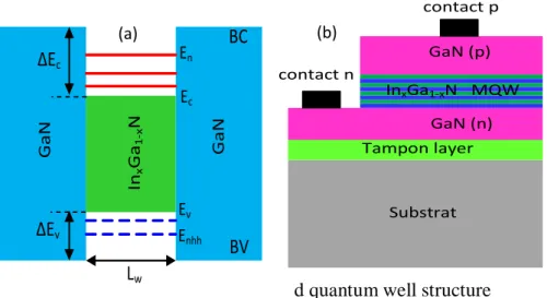
The quantum wells are thin layered semiconductor structures in which one semiconductor well material is surrounded by two "barrier" layers with a wider band gap (Eg1< Eg2). Since, the well is so thin, typically about 100 Å, both electrons and holes are confined. The energy states allowed for the carriers are quantified. The direct advantage of this configuration is to reduce the active volume, which makes it easier to reach a population inversion, the threshold for oscillation and increase the probability of transitions.
The quantum physic equations are valid when the active layer thickness is of the order of few nanometers and becomes comparable to the De Broglie wavelength λF=2πℏ(2mEF)-1/2 , m is the electron effective mass, EF refers to the Fermi level [10,11]. In the type I quantum well, the electrons and holes are confined within the same spatial region as shown in figure 1(a,b). [12].
Fig. 1. (a,b) InGaN/GaN based quantum well structure
By varying the well width and the alloy composition, the quantification energy levels can be tuned to modify the emission wavelength of the structure. Indeed, the shift between two subbands of the same quantum number n can be approximated by the equation given in reference [13]. The carrier confinement energies (electrons and holes) in quantum wells are obtained when solving the corresponding Schrödinger equation [14].The resolution of the Schrödinger equation requires the knowledge of the structural potential V(z) seen by the particle along the direction of interest z [15].The solution of Schrödinger equation gives an improved estimate of the energy eigenvalue with variable En the quantification energy. In order to determine the quantization energies, the numerical method of dichotomy is used. When the Electron confinement energies are not negligible in front of the height of the
GaN GaN In x Ga 1 -x N Lw BC BV ΔEc ΔEv En Ec Enhh Ev Substrat GaN (n) GaN (p) InxGa1-xN MQW Tampon layer contact p contact n (a) (b)
potential barrier, either because of ΔEc is not very important or Lw is small. By asking V0=ΔEc , the potential may be written as mentioned in [16]. Schrödinger’s equation in the three regions is given by [17]. The epitaxial growth techniques of lattice mismatched materials became well controlled,. Thus, the lattice matching is not an imperative; moreover the strain effects are exploited in many high performance electronic and optoelectronic components. Indeed, the use of strained heterostructures changes the energy position of both conduction band and valence band and gives us the possibility to adjust the emission wavelength [17]. In the pseudomorphic growth along the (001) direction, the difference of lattice constants for the quantum well and barrier layers, results in a parallel ɛxx and a perpendicular strain ɛz [17]. The energy offset of gravity centers of the conduction band and the valence band in k=0vary proportionally with the strain [18].The energy offset induced by the shear strain for the valence band gap [18-20]. The material gain per unit propagation length G(hω), is defined as the fractional increase of the photon-flux density propagating along the direction of interest in the crystal [7]. The gain is calculated using [21,22].
2. RESULTS AND DISCUSSION
Figure 2 shows the variation of the unstrained bandgap energy as a function of the indium concentration. The bandgap is equal to 3.05eV for an indium concentration of x=0.10. When it reaches the value of 0.3, the bandgap energy is 2.6 eV. So, we note a decrease in the
bandgap energy with about ΔEg = 0.45eV. The effect of the strain on the bandgap energy is
also distinguished. The strain induced a decrease in the bandgap energy and makes the
valence bands ΔEghh strongly anisotropic. For an indium value of x = 0.30, the strain bandgap
energy is equal to 2.43 eV with a deformation of ɛ = 3%. So, the strain induces a decrease of
the bandgap of about ΔEghh = 0.17eV. As seen from figure 2, when the indium concentration
becomes important x=0.40, we will have a compressive strain ɛ=4%, which makes the structure unstable. The results of simulations are very according to the experimental one.
Fig.2. Variation of the bandgap energy as a function of the indium concentration.
Figures 3 (a,b) illustrate the variation of electron confinement energies for the InxGa1-xN/GaN
quantum well structure as a function of the well width (Lw) for different indium
concentrations. It is noted that the increase in the well width Lw induces a decrease in the quantized energy. On the other hand, the increase of the indium concentration x increases the number of the confinement energy levels. This leads to an increase of the transition probability of the direct electron-hole transitions. Figures 4 (a,b) present the heavy hole confinement energies of the InxGa1-xN/GaN quantum well structure as a function of the well width for different indium contents. The heavy hole confinement energies increase with reducing the well width. Figures 5 (a, b) show the calculated transition energies occurred
between the conduction band and the heavy holes band in the InxGa1-xN/GaN quantum well
structure versus the well width for different concentrations of indium. It is observed that the increase of the well width, leads to a decrease of the transition energy.
0.05 0.1 0.15 0.2 0.25 0.3 0.35 0.4 1.8 2 2.2 2.4 2.6 2.8 3 3.2 3.4 3.6 In composition E g ( e V ) Eg strain(x) Eg(x) C. A. Parker [20] 0 0.2 0.4 0.6 0.8 1 -0.1 -0.08 -0.06 -0.04 -0.02 0 In composition (x ) T=300K
Fig.3. Variation of electron confinement energies levels according to the well width Lw a) x=0.10 b) x=0.30
Fig.4. Variation of heavy holes confinement energies levels according to the well width Lw a) x=0.10 b) x=0.30
Fig.5. Variation of transition energy according to the well width Lw a) x=0.10 b) x=0.30 0 2 4 6 8 10 12 14 16 18 20 0.05 0.1 0.15 0.2 0.25 0.3 0.35 0.4 L w (nm) En e (e V ) x=0.1 level 1 level 2 level 3 level 4 level 5 level 6 (a) 0 2 4 6 8 10 12 14 16 18 20 0 0.05 0.1 0.15 0.2 0.25 0.3 0.35 0.4 0.45 L w (nm) En e ( e V ) x=0.3 level 1 level 2 level 3 level 4 level 5 ( b ) 0 2 4 6 8 10 12 14 16 18 20 0 0.02 0.04 0.06 0.08 0.1 0.12 0.14 0.16 Lw (nm) En h h (e V ) x=0.1 level 1 level 2 level 3 level 4 level 5 ( a ) 0 2 4 6 8 10 12 14 16 18 20 0 0.05 0.1 0.15 0.2 0.25 0.3 0.35 0.4 0.45 L w (nm) En h h ( e V ) x=0.3 level 1 level 2 level 3 level 4 level 5 level 6 ( b ) 0 2 4 6 8 10 12 14 16 18 20 3 3.1 3.2 3.3 3.4 3.5 3.6 3.7 Lw (nm) En e --h h ( e V ) x=0.1 HH1-C1 HH2-C2 HH3-C3 HH4-C4 ( a ) 0 2 4 6 8 10 12 14 16 18 20 2.4 2.6 2.8 3 3.2 3.4 3.6 L w (nm) E n e --h h ( e V ) x=0.3 HH1--C1 HH 2--C2 HH3--C3 HH4--C4 ( b )
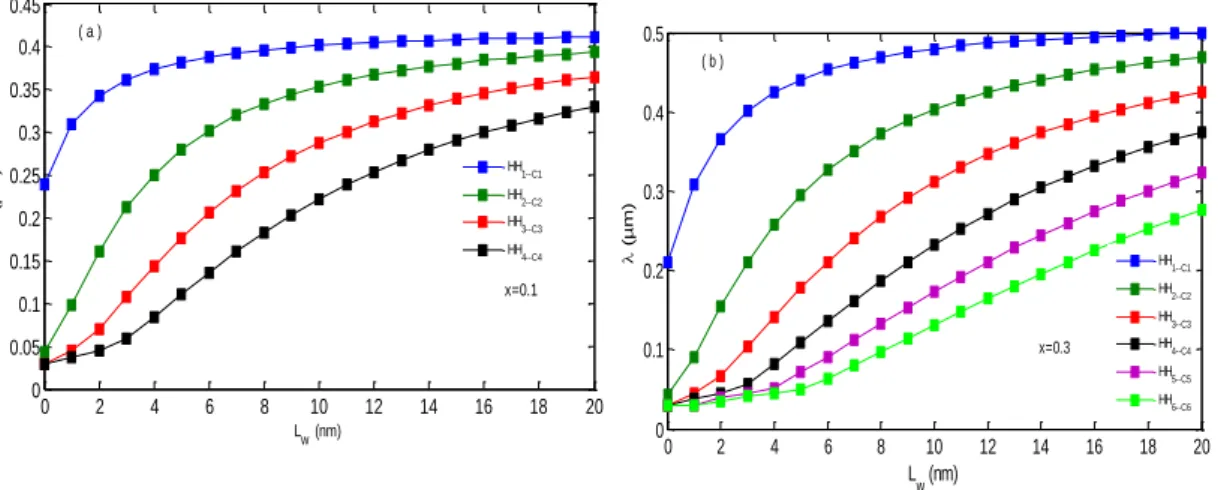
Figures 6 (a, b) illustrate the variation of emission wavelengths as a function of the quantum well width Lw for different indium mole fractions. It is noted that increasing the well width induces an increase of the wavelength. When the indium concentration increases, the emission wavelength varies from 0.1 to 0.5 μm. For example, for a thickness well of 8 nm and an indium concentration x = 0.10, the emission wavelength λe1-hh1 is 0.396 μm. For the same
transition e1-hh1and an indium content of x=0.30, the emission wavelength becomes 0.469μm.
Fig.6. Variation of the wavelength according to well width Lw
a) x=0.10 b) x=0.30
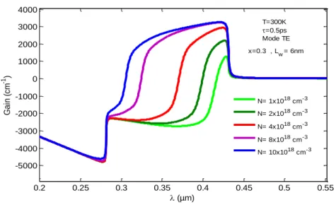
Figure 7 shows the optical gain variation as a function of the emission wavelengths for a 6nm In0.3Ga0.7N/GaN quantum well structure and different carrier densities N. It can be seen that the optical gain increases with increasing carrier density to achieve the saturation for N=8x1018cm-3. It can be seen that more the carrier injection becomes larger, more the spectral width Δλ increases significantly. Figure 8 shows the evolution of optical gain versus the wavelength. An increase of the well width leads to a decrease of the maximum optical gain. However, the spectral width becomes large and the emission wavelength achieves the value of 0.5μm. For example, if the thickness of the quantum well is varied from 6 to 10 nm, the
maximum optical gain decreases through 976 cm-1.
0 2 4 6 8 10 12 14 16 18 20 0 0.05 0.1 0.15 0.2 0.25 0.3 0.35 0.4 0.45 Lw (nm) ( µ m ) x=0.1 HH1--C1 HH2--C2 HH3--C3 HH4--C4 ( a ) 0 2 4 6 8 10 12 14 16 18 20 0 0.1 0.2 0.3 0.4 0.5 L w (nm) ( µ m ) x=0.3 HH1--C1 HH2--C2 HH3--C3 HH4--C4 HH5--C5 HH6--C6 ( b )
Fig.7. Variation of optical gain versus wavelength for different electron densities
Fig.8. Variation of optical gain versus wavelength for different widths Lw
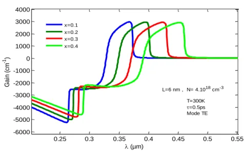
Figure 9 shows the optical gain variation as a function of the emission wavelength for several indium concentrations in the InxGa1-xN/GaN active zone with an injected carrier density N=4.1018 cm-3 at room temperature and a well width of 6 nm. It is noted that the increase in the indium concentration induces a shift of the gain spectra towards long wavelengths. For an increasing of the indium concentration from 0.10 to 0.30, the emission wavelength shifts from 0.365 to 0.425μm. 0.2 0.25 0.3 0.35 0.4 0.45 0.5 0.55 -5000 -4000 -3000 -2000 -1000 0 1000 2000 3000 4000 (µm) G a in ( cm -1 ) x=0.3 , Lw= 6nm N= 1x1018 cm-3 N= 2x1018 cm-3 N= 4x1018 cm-3 N= 8x1018 cm-3 N= 10x1018 cm-3 T=300K =0.5ps Mode TE 0.2 0.25 0.3 0.35 0.4 0.45 0.5 0.55 -5000 -4000 -3000 -2000 -1000 0 1000 2000 3000 4000 (µm) G a in ( cm -1 ) x=0.3 N= 4.1018 cm-3 Lw= 5 nm Lw= 6 nm Lw= 8 nm Lw= 10 nm T=300K =0.5ps Mode TE
Fig.9. Variation of optical gain versus wavelength for different concentrations x
Fig.10. Variation of optical gain versus wavelength for different temperatures T
Figure 10 shows the optical gain variation as a function of the wavelength. It is noted that the increase in temperature leads to a significant decrease of the maximum optical gain. When the
temperature increases from 300 to 400K, the maximum gain decrease from 2936 to 2698 cm
-1
, that is to say, we have a loss of Gmax= 238cm-1. From this study, we can optimize the quantum well structure based on InxGa1-xN/GaN to achieve a reliable optoelectronic component emitting around 400nm. It suffices to find a compromise between the well width, the indium mole fraction, the carrier density and the temperature.
0.25 0.3 0.35 0.4 0.45 0.5 0.55 -6000 -5000 -4000 -3000 -2000 -1000 0 1000 2000 3000 4000 (µm) G a in ( cm -1 ) L=6 nm , N= 4.1018 cm-3 x=0.1 x=0.2 x=0.3 x=0.4 T=300K =0.5ps Mode TE 0.2 0.25 0.3 0.35 0.4 0.45 0.5 -2000 -1000 0 1000 2000 3000 4000 (µm) G a in ( c m -1) T=200K T=300K T=400K T=500K 200 250 300 350 400 450 500 2400 2600 2800 3000 3200 T G m a x (c m -1) Lw=6nm x=0.30 N=4x1018cm-1 Mode TE =0.5ps
4. CONCLUSION
In this paper, a theoretical study has been carried out. Simulations have been performed for the design and optimization of an InGaN/GaN strained quantum well structures. In our study, the effects of ɛ(x) and x on the bandgap energy, the quantum confinement energies, the transition energy and the wavelength emission are taken into account. Then, we have studied the material gain a based InGaN/GaN quantum well material system and present the factors that influence the material gain performance as well width, electron density, x concentration and temperature T. The optimized InGaN/GaN quantum well structures have better optical
properties with a maximum optical gain of 2936 cm-1 and an emitting wavelength of 423 nm,
at a well width of 6 nm, injected electron density N=4x1018cm-3, x=0.30, and a room temperature T=300K.This work allows us the possibility to realize a strained multiple quantum well VCSEL structure emitting in the blue region of the electromagnetic spectrum. REFERENCES
[1] S. Mokkapati, C. Jagadish, III-V compound SC for optoelectronic devices, Materialstoday Volume 12, Issue 4, (2009), 22-32
[2] H. J. Joyce, Q. Gao, H. Hoe Tan, C. Jagadish, Y. Kim, J. Zou, L. M.Smith, H. E. Jackson, J. M. Yarrison-Rice, P. Parkinson, M. B. Johnston, III–V semiconductor nanowires for optoelectronic device applications, Progress in Quantum Electronics, Volume 35, Issues 2–3 (2011), 23-75
[3] Mohamed Sellahi, Laser `a semi-conducteur III-V `a´émission verticale de haute cohérence et de forte puissance : Etat vortex, continuum et bi-fréquence THz, thèse de doctorat, 34095 Montpellier, France, (2014).
[4] D. Xiao and k.W. Kim,” Envelope-function analysis of wurtzite InGaN/GaN quantum well light emitting diodes: JA P, Vol-96 No. 1, (2004)
[5] S. K. Jana, S. Ghosh , S. M. Dinara, T. D. Das and D. Biswas, Strain Effects on Band Structure of Wurtzite InGaN/GaN Quantum Well on Si Substrate, IOP Conf. Series: Materials Science and Engineering 73 (2015) 012151
[6] S.Calvez, J. E. Hastie, M. Guina, O. G. Okhotnikov and M. D Dawson, Semiconductor disk lasers for the generation of visible and ultraviolet radiation. Laser & Photonics Reviews, vol. 3, no. 5, (2009) 407–434
[8] A. Fisher, H.Kuhn and H.Richter, New approach in equilibrium theory for strained layer relaxation. Phys. Rev. Lett. 73, (1994) 2712–2715
[9] C. A. Broderick, M. Usman, E.P. O'Reilly, 12 band k·p model for dilute bismide alloys of (In)GaAs derived from supercell calculations, physica status solidi (b),Volume 250, Issue 4 (2013 ) 773–778.
[10] H. Y. Fan, "Temperature Dependence of the Energy Gap in Semiconductors," Phys. Rev., vol. 82, (1951) 900
[11] J. Piprek, Semiconductor Optoelectronic Devices: Introduction to Physics and Simulation. California: Academic Press, 2003
[12] D. E. Aspnes, GaAs lower conduction-band minima: Ordering and properties. Phys. Rev. B. 14, (1976) 5331–5343
[13] P.S. Zory. Quantum well lasers. Optics and Photonics Series, Academic Press, 1993 [14] BragVinter, Optoelectrique, Emanuel Rosencher, Masson, 1998
[15] B,R, Nag L.R.Carley, G.Declerck, F.M.K Laass en, Physics of quantum Well Devices, Kluwer Academic Publishers, 2002
[16] Henry Mathieu & Harvéfanet, physique des semi-conducteurs et des composants électroniques, Dunod 4e édition, 2001
[17] Maurice G. A. Bernard, Georges Duraffour, Laser Conditions in Semiconductors, physica status solidi (b) Volume 1, Issue 7 (1961) 699–703
[18] Yvan cuminal, Réalisation et etude de diodes lazers à base de GaSb émettant vers 2.3 µm pour application à l’analyse de gaz, Université Montpellier II, 1997
[19] J. Wu, W. Walukiewicz, K. M. Yu, J. W. Ager III, E. E. Haller, H. Lu, and W. J. Schaff. Small bandgap bowing in In1-xGaxN alloys. Applied Physics Letters, 80(25) (2002) 4741– 4743,
[20] C. A. Parker, J. C. Roberts, S. M. Bedair, M. J. Reed, S. X. Liu, N. A. El-Masry, and L. H. Robins. Optical bandgap dependence on composition and thickness of InxGa1-xN (0 < x < 0.25) grown on GaN. Applied Physics Letters, 75(17), (1999) 2566–2568
[21] I. P. Marko, C. A. Broderick, S. Jin, P. Ludewig, W. Stolz, K.Volz, J.M. Rorison, E. P. O’Reilly, S.J. Sweeney, Optical gain in GaAsBi/GaAs quantum well diode lasers, scientific Reports (2016) 1-10
[22] Broderick, C. A., Harnedy, P. E. & O’Reilly, E. P. Theory of the Electronic and Optical Properties of Dilute Bismide Quantum Well Lasers. IEEE J. Sel. Top. Quantum Electron. 21(6), (2015) 1503313