HAL Id: lirmm-01430800
https://hal-lirmm.ccsd.cnrs.fr/lirmm-01430800
Submitted on 10 Jan 2017
HAL is a multi-disciplinary open access
archive for the deposit and dissemination of sci-entific research documents, whether they are pub-lished or not. The documents may come from teaching and research institutions in France or abroad, or from public or private research centers.
L’archive ouverte pluridisciplinaire HAL, est destinée au dépôt et à la diffusion de documents scientifiques de niveau recherche, publiés ou non, émanant des établissements d’enseignement et de recherche français ou étrangers, des laboratoires publics ou privés.
A Bulk Built-in Sensor for Detection of Fault Attacks
Rodrigo Possamai Bastos, Franck Sill Torres, Jean Max Dutertre, Marie-Lise
Flottes, Giorgio Di Natale, Bruno Rouzeyre
To cite this version:
Rodrigo Possamai Bastos, Franck Sill Torres, Jean Max Dutertre, Marie-Lise Flottes, Giorgio Di Natale, et al.. A Bulk Built-in Sensor for Detection of Fault Attacks. HOST: Hardware-Oriented Security and Trust, Jun 2013, Austin, TX, United States. pp.51-54, �10.1109/HST.2013.6581565�. �lirmm-01430800�
A Bulk Built-in Sensor for Detection of Fault Attacks
R. Possamai Bastos1, F. Sill Torres2, J.-M. Dutertre3, M.-L. Flottes4, G. Di Natale4, B. Rouzeyre41
TIMA Laboratory (Grenoble INP, UJF, CNRS), Grenoble, France ([email protected])
2
UFMG (Dept. of Electronic Engineering), Belo Horizonte, Brazil ([email protected])
3
Centre Microélectronique de Provence - Georges Charpak, Gardanne, France ([email protected])
4
LIRMM (Université Montpellier II / CNRS UMR 5506), Montpellier, France ({flottes, dinatale, rouzeyre}@lirmm.fr)
Abstract—This work presents a novel scheme of built-in current
sensor (BICS) for detecting transient fault-based attacks of short and long duration as well as from different simultaneous sources. The new sensor is a single mechanism connected to PMOS and NMOS bulks of the monitored logic. The proposed protection strategy is also useful for improving any state-of-the-art Bulk-BICS from pairs of PMOS and NMOS sensors to single sensors.
Keywords: Built-in current sensors, concurrent detection, fault attacks, fault tolerance, security, soft errors, transient faults
I. INTRODUCTION
Integrated systems based on ultra-deep submicron technologies require higher robustness to natural aging processes or radiation environmental sources [1]. In addition to these natural phenomena, malicious fault-based attacks can be used to bypass security mechanisms of secure systems and to extract information from confidential data [2]. Both these natural or malicious phenomena on integrated circuits can induce transient effects that provoke bit-flips of stored results during the system lifetime. Until the early 2000’s, researches about how to mitigate these issues were focused mostly on concurrent error detection and/or correction mechanisms to cope with soft errors induced by transient faults in memory cells. In the last decade, however, more sensitive nanotechnologies as well as the increasing demand for secure systems have also pushed for the development of countermeasures against transient faults in combinational parts of the circuits. These faults indeed can propagate up to storage elements and thus cause soft errors as well. On the other hand, if the transient fault does not induce any error due to an electrical, logical or latching-window masking effect, its detection is crucial all the same in secure applications since the fault itself reveals an attempt of attack.
Among the several strategies to detect transient faults caused by radiation or optical sources, Bulk Built-In Current Sensors (BBICS) offer a promising solution that is perfectly suitable for system design
flows based on CMOS standard cells of commercial libraries. BBICS have the high detection efficiency of costly fault-tolerance schemes (e.g. duplication with comparison) with the low area and power overheads of less efficient mitigation techniques such as time redundancy approaches [3][4][5][6]. Without impacting on system operating frequency, BBICS deal with transient faults of short and long duration as well as multiple faults. Furthermore, as they closely monitor the zones where the faults arise, an early detection is possible immediately after a fault occurrence, preventing induction and propagation of errors to other clock cycles or system blocks.
All today’s BBICS-based strategies [5][6][7][8] [9][10] use two different circuits that monitor independently PMOS and NMOS bulk currents from pull-up and pull-down CMOS networks. We present in section III of this paper a new lower-area BBICS scheme compounded of a single circuit that is able to monitor at the same time both CMOS networks. Important preliminary related information regarding transient faults and built-in current sensors is initially discussed in section II.
II. FUNDAMENTALS
A. Transient Faults in Integrated Circuits
Transient voltage variations during the lifetime of combinational or sequential circuits are defined as transient faults. The first harmful effects of transient faults are soft errors by inverting stored results of system operations (i.e. bit-flips of storage elements). As consequences of transistor shrinking and growing communication of confidential data, soft errors can happen today even at ground level by means of perturbation events arisen from environmental or intentional sources. Examples of environment events are alpha particles released by radioactive impurities and more importantly neutrons from cosmic rays [1].
On the other hand, intentional perturbation events are usually produced by optical sources such as flashlights or laser beams [2] that can maliciously induce transient effects on secure circuits like smartcards to retrieve their secret information.
Soft errors and transient faults are also known as single event upsets (SEU) and single event transients (SET) in fault-tolerance-related fields. If provoked by malicious fault-based attacks, such circuit misbehaviors provide fundamental information for cryptanalysis methods that are able to break security applications.
B. BICS Detecting Transient Faults
Built-In Current Sensors (BICS) were initially proposed as a mechanism for detecting large increases in the current IDDQ consumed by a CMOS
circuit during its quiescent state, i.e. when the circuit is not switching. The mechanism allows thus testing CMOS circuits against permanent faults [11]. Further, BICS were also adapted for detecting transient faults in memory cells (i.e. bit-flips) [12][13][14][15]. Recently, efforts were made for monitoring transient faults in combinational logic as well [16]. All these techniques connect BICS to the power lines (VDD and GND) of the monitored circuit
to distinguish anomalous transient currents from normal currents. Today’s problem is the amplitude of transient currents induced by radiation effects or fault attacks have the same order of magnitude than currents normally generated by switching activities in combinational logic circuits. Hence, schemes monitoring power lines are very limited for detecting just small range of transient faults.
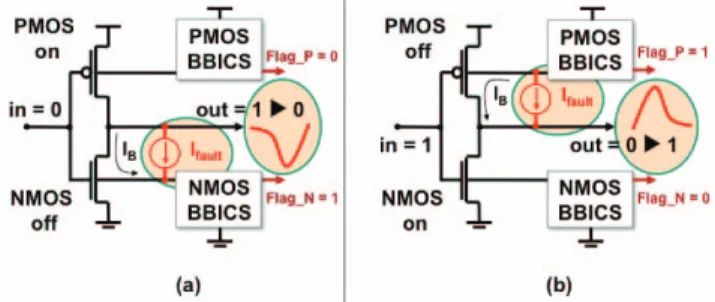
On the other hand, a wide range of transient faults is detectable whether BICS are connected to the bulks of the monitored circuit’s transistors; such a smart idea was introduced for the first time in [7][17]. Fig. 1 (a) and (b) illustrate Bulk BICS (BBICS) identifying anomalous transient currents
Ifault that flow through the junction between a bulk
and a reversely biased drain of a disturbed transistor (MOSFETs “off” in Fig. 1). BBICS indeed take advantage of two facts: (1) In fault-free scenarios (i.e. Ifault = 0) the bulk-to-drain (or drain-to-bulk)
current IB is negligible even if the MOSFET is
switching in function of new input stimuli; (2) During transient-fault scenarios, Ifault is much higher
than the leakage current flowing through the junction. The range of detectable transient faults is
easily adjustable by calibrating the size of the transistors that constitute the BBICS. Hence, schemes based on BBICS can be designed to latch a flag of fault indication for abnormal currents within a defined range that represents a risk of resulting in soft errors.
Figure 1. The two classic cases of transient faults in a CMOS inverter perturbed by an anomalous current Ifault
Note in Fig. 1 that the connections between monitored circuit (e.g. inverter) and PMOS and NMOS BBICS blocks are done by using metal – from the body-ties of each monitored transistor (i.e. transistor bulks of the inverter) up to the inputs of the BBICS circuitries. Thereby, peaks of anomalous transient currents (i.e. transient faults) are almost not attenuated [18], ensuring thus enough signals for BBICS performing an efficient detection. The only small attenuation is a function of the local distance between the struck zone of the monitored transistor and its body-tie.
III. NEW SINGLE BBICS A. Strategy for Protecting a System
The classic BBICS-based strategy is using a pair of sensors (PMOS and NMOS) to monitor pull-up and pull-down networks – e.g. PMOS-BBICS 1 and NMOS-BBICS 1 in Fig. 2 (a). The capacity of each sensor for identifying transient faults is limited to a certain number of monitored transistors. Hence the strategy is also splitting the target system into blocks with the maximum possible number of transistors the sensor is able to monitor. Fig. 2 (a) illustrates an example of system (chains of inverters) divided into two blocks that are monitored by two pairs of BBICS. For the same example, our strategy is otherwise to use single sensors for up and pull-down networks as Fig. 2 (b) shows.
B. Structure of Sensor
The circuit structure of any BBICS is composed of two main parts. One is a memory element (e.g. a
Figure 2. (a) The classic BBICS-based strategy with pairs of BBICS (NMOS and PMOS) monitoring blocks of a system; and (b) Our strategy with
the new single BBICS able to check both pull-up and pull-down networks
latch) responsible for registering a flag in case of fault. The other part is a set of transistors that constitute the input circuit of the sensor. It receives the metal connections coming from the body-ties of each monitored transistor. In function of the type of input circuit we classify existing BBICS structures into two groups: (1) High fault-detecting capacity
sensors [6][7][8] just slightly modify the bulk
capacitance of the monitored transistors by using a small input circuit connected to them; thereby these sensors are more capable to recognize a wider range of transient faults. On the contrary, they create an offset on the bulk voltage of the monitored transistors at normal operation (i.e. in fault-free scenarios). It results in slightly lower threshold voltage that represents higher sub-threshold leakage currents [6]; and (2) Low sub-threshold leakage
sensors [5][7][9][10] avoid any voltage offset on the
bulk by connecting it via a high ohmic transistor (large channel length) in on-state with Vdd or gnd.
On the other hand, they considerably increase the bulk capacitance and, thus, decrease their fault-detecting capacities.
The structure of the new single BBICS presented in this paper takes the high fault-detecting capacity of the sensors proposed in [6] and illustrated in Fig. 3 (a). Moreover, it was optimized from a pair of sensors to a single sensor and, consequently, the area could be significantly reduced as we can see in Fig. 3 (b) compared with Fig. 3 (a) in terms of transistor counting. Low leakage power overheads can be met by finding an optimal number of monitored transistors. In Fig. 3, Wmin represents the minimum
diffusion width of the transistors, Lmin is the
minimum channel length, and design factors Xn, Yn,
Xp, Yp, X and Y are used for calibrating the sensor
with a desired fault-detecting capacity.
Transistors 5, 6, 7, and 8 in Fig. 3 (b) constitute the latch used to memorize a flag (i.e. output Flag at
Vdd) in case of a transient fault within a defined
range of current that temporally perturbs the monitored pull-up or pull-down network. In addition, the latch transistors are responsible for amplifying the anomalous transient currents coming from node NMOS_Bulk or going to node
PMOS_Bulk of monitored blocks. Factors X and Y
allow increasing the gain of amplification and, thus, configuring the sensor with higher fault-detecting capacity. Transistors 11 and 12 are used to set the sensor in sleep-mode when the system is left on standby (i.e. signal Sleep_Mode at Vdd). It leads to
zero the offset on the bulk voltage of the monitored block, and so the sub-threshold leakage power consumption is significantly reduced.
C. Mode of Operation
In fault-free conditions and inactive sleep mode (i.e. Sleep_Mode at gnd), the proposed structure in Fig. 3 (b) has in theory NMOS_Bulk at gnd level and
PMOS_Bulk at Vdd. Signal Flag is at gnd; node1 at Vdd; and transistors 1, 3, 4, 10, 11, and 12 are in
off-state. Further, as transistors 2 and 9 are in on-state, they impose, in reality, on NMOS_Bulk and
PMOS_Bulk a small voltage drop.
In case of a transient fault in the pull-up network of the monitored block, PMOS_Bulk acts as a current sink, i.e. a transient current flows from
node1 to PMOS_Bulk through transistor 9. Thereby
the voltage of node1 decreases, leading the inverter formed by transistor 6 and 5 to flip and signal Flag to change from gnd to Vdd. As consequence, the
other inverter (i.e. transistor 7 and 8) also switches forcing node1 to gnd even after the transient fault has ceased. Moreover, it activates transistors 10 and 1 in order to set the normal operation levels for
PMOS_Bulk and NMOS_Bulk (i.e. Vdd and gnd)
during such a state of fault indication at Flag. As soon as this flag is processed by higher instances of the system, it must be reset (i.e. input Reset at Vdd) to
be able to detect again other transient faults.
If a fault happens in the pull-down network of the monitored block, a transient current flows through
Figure 3. (a) Strucutres of a BBICS pair (NMOS and PMOS) proposed in [6]; and (b) the structure of our new single BBICS
transistor 2 coming from NMOS_Bulk and, consequently, the same procedure described above is performed to register an indication of fault (i.e. signal Flag from gnd to Vdd). Note that if other
transient fault occurs simultaneously in pull-up network, the single BBICS is able to accomplish the memorization of a flag since the sense of the positive feedback is the same for both fault events. On the contrary, no new transient fault can be detected when a flag of fault is latched or during the reset of the sensor.
IV. CONCLUSIONS
With a count of only 12 transistors for monitoring PMOS and NMOS networks, the new BBICS proposed in this paper presents lower area than previous versions. No additional logic is required to keep, refresh, or gather the fault indications from CMOS networks. Moreover, the number of total transistors can be reduced to 9 by eliminating one of the reset transistors and the sleep mode. Ongoing works are the fabrication of a prototype and the validation of the approach using a laser beam.
V. REFERENCES
[1] T. Karnik, P. Hazucha, and J. Patel, “Characterization of Soft Errors Caused by Single Event Upsets in CMOS Processes”, IEEE Transactions on Dependable and Secure Computing, v.1, n.2, pp. 128-143, 2004. [2] R. Leveugle, “Early Analysis of Fault-Based Attack Effects in Secure
Circuits”, IEEE Transactions on Computers, v.56, n.10, pp. 1431-1434, 2007.
[3] C. Lisboa et al., “Using Built-in Sensors to Cope with Long Duration Transient Faults in Future Technologies”, in Proc. ITC, IEEE, 2007, pp. 1-10.
[4] R. P. Bastos et al., “How to Sample Results of Concurrent Error Detection Schemes in Transient Fault Scenarios?”, in Proc. RADECS, IEEE, 2011, pp. 635-642.
[5] F. S. Torres, R. P. Bastos, “Robust Modular Bulk Built-In Current Sensors for Detection of Transient Faults”, in Proc. SBCCI, IEEE, 2012, pp. 1-6.
[6] R. P. Bastos et al., “Novel transient-fault detection circuit featuring enhanced bulk built-in current sensor with low-power sleep-mode”, Elsevier Microelectronics Reliability, v. 52, n. 9-10, pp. 1781-1786, Sep.-Oct. 2012.
[7] E. H. Neto et al., “Using Bulk Built-in Current Sensors to Detect Soft Errors”, IEEE Micro, v. 26, n. 5, pp. 10–18, Sep. 2006.
[8] E. H. Neto et al., “Tbulk-BICS: A Built-In Current Sensor Robust to Process and Temperature Variations for Soft Error Detection”, IEEE Transactions on Nuclear Science, v. 55, n. 4, pp. 2281-2288, Aug. 2008. [9] Z. Zhang et al., “A Bulk Built-In Voltage Sensor to Detect Physical
Location of Single-Event Transients”, JETTA, Springer, March 2013. [10] A. Simionovski, G. Wirth, “Simulation Evaluation of an Implemented
Set of Complementary Bulk Built-In Current Sensors with Dynamic Storage Cell”, IEEE Transactions on Device and Materials Reliability, v. PP, n. 99, 2013.
[11] S. P. Athan et al., “A Novel Built-in Current Sensor for IDDQ Testing of
Deep Submicron CMOS ICs”, in Proc. VTS, IEEE, 1996, pp. 118-123. [12] J. Lo et al., “Design of Static CMOS Self-checking Circuits using
Built-In Current Sensing”, in Proc. FTCS, IEEE, 1992, pp. 104-111. [13] F. Vargas, M. Nicolaidis, “SEU-tolerant SRAM design based on current
monitoring”, in Proc. FTCS, IEEE, 1994, pp.106-115.
[14] B. Gill et al., “An Efficient BICS Design for SEUs Detection and Correction in Semiconductor Memories”, in Proc. DATE, IEEE, 2005, pp. 592-597.
[15] P. Ndai et al., “A Soft Error Monitor Using Switching Current Detection”, in Proc. ICCD, IEEE, 2005, pp. 185-190.
[16] A. Narsale, M. C. Huang, “Variation-tolerant hierarchical voltage monitoring circuit for soft error detection”, in Proc. ISQED, IEEE, 2009, pp. 799-805.
[17] E. H. Neto et al., “Evaluating Fault Coverage of Bulk Built-in Current Sensor for Soft Errors in Combinational and Sequential Logic”, in Proc. SBCCI, IEEE, 2005, pp. 62-67.
[18] G. Wirth, “Bulk built in current sensors for single event transient detection in deep-submicron technologies”, Elsevier Microelectronics Reliability, v. 48, n. 5, pp. 710-715, May 2008.

![Figure 3. (a) Strucutres of a BBICS pair (NMOS and PMOS) proposed in [6]; and (b) the structure of our new single BBICS](https://thumb-eu.123doks.com/thumbv2/123doknet/12270604.321600/5.918.101.816.71.399/figure-strucutres-bbics-nmos-proposed-structure-single-bbics.webp)
