HAL Id: hal-01727137
https://hal.archives-ouvertes.fr/hal-01727137
Submitted on 15 Feb 2021
HAL is a multi-disciplinary open access
archive for the deposit and dissemination of
sci-entific research documents, whether they are
pub-lished or not. The documents may come from
teaching and research institutions in France or
abroad, or from public or private research centers.
L’archive ouverte pluridisciplinaire HAL, est
destinée au dépôt et à la diffusion de documents
scientifiques de niveau recherche, publiés ou non,
émanant des établissements d’enseignement et de
recherche français ou étrangers, des laboratoires
publics ou privés.
Does the Rashba splitting in CH 3 NH 3 PbBr 3 arise
from 2x2 surface reconstruction?
Xiaoyang Che, Boubacar Traoré, Claudine Katan, Mikael Kepenekian, Jacky
Even
To cite this version:
Xiaoyang Che, Boubacar Traoré, Claudine Katan, Mikael Kepenekian, Jacky Even. Does the Rashba
splitting in CH 3 NH 3 PbBr 3 arise from 2x2 surface reconstruction?. Physical Chemistry
Chemi-cal Physics, Royal Society of Chemistry, 2018, 20 (14), pp.9638-9643. �10.1039/C8CP00745D�.
�hal-01727137�
Cite this: Phys. Chem. Chem. Phys., 2018, 20, 9638
Does Rashba splitting in CH
3
NH
3
PbBr
3
arise
from 2 ! 2 surface reconstruction?†
Xiaoyang Che,
abBoubacar Traore,
aClaudine Katan,
aMikae¨l Kepenekian
*
aand Jacky Even
*
bAs a result of early theoretical predictions, evidence for the Rashba or Dresselhaus effect in hybrid perovskites has recently attracted several experimental investigations, motivated by possible applications in spin-orbitronics. For instance, a large Rashba splitting has recently been reported for the (001) surface of CH3NH3PbBr3. This effect is forbidden in the bulk material since both low-temperature and room-temperature crystal structures present inversion symmetry. Here we investigate the effects of two (001) nanoscale surface reconstructions of CH3NH3PbBr3using first-principles approaches based on density functional theory (DFT). The two experimental reconstructions are related to different orientations of MA cations at the surface, defining zigzag and dimer phases. The impact of these structural transformations on their electronic structures is thoroughly investigated. Whereas calculations reveal the occurrence of surface-induced Rashba effect, its amplitude is considerably smaller than the experimentally reported value, in agreement with other experimental investigations and leading to the conclusion that mesoscale surface polar domains and/or surface defects may result from sample preparation.
1 Introduction
Solution-processed halide perovskites have recently led to solar cells with outstanding power conversion efficiencies and low costs of production. Their highest record of light to electricity conversion efficiency has witnessed a spectacular increase from
3.8% in the pioneering work of Miyasaka and co-workers1in
2009 to 22.7% (NREL certificated) in 2017,2,3surpassing that of state-of-the-art thin film silicon based solar cells.4,5 Very recently, fully inorganic perovskite quantum dots (CsPbI3) also led to the record efficiency of the quantum dot cell technology.2,6 More, their bulk and colloidal nanostructures present attractive photo- and electroluminescence properties with unusual giant relativistic effects in their band structures, which opened new paths in the field of optoelectronics.7–10 However, fundamental studies remain essential in order to shed more light on the microscopic mechanisms at the origin of their exceptional optoelectronic properties.
One main feature of halide perovskites is the presence of heavy atoms such as lead, tin or iodine that leads to a strong spin–orbit coupling (SOC) effect.11–14 Combining this effect
with the loss of inversion symmetry gives rise to strong spinor splitting of Rashba, Dresselhaus or mixed Rashba–Dresselhaus
types15–17 in both or either the conduction and valence
bands.13,18–22 Such an effect would open the way to halide
perovskite-based spintronics and spin-orbitronics.23,24 Direct evidence for the Rashba effect in hybrid perovskites was recently inspected using angle-resolved photoemission spectroscopy (ARPES) on CH3NH3PbBr3(MA = CH3NH3+) single crystals, which delivered contradictory outcomes.25,26 Both experiments were per-formed on the (001) surfaces of MAPbBr3. Whereas Komesu et al.25 did not evidence any effect related to k-dependent spin-splitting in their room temperature experiments, Niesner et al.,26 after great care in sample surface preparation, reported giant splittings of 7 " 1 eV Å and 11 " 4 eV Å for low temperature orthorhombic and high temperature cubic phases, respectively. To the best of our knowledge, these values correspond to the largest Rashba effects ever recorded by ARPES. Meanwhile, specific patterns of the orientations of MA have been observed on the (001) surface of MAPbBr3 by scanning tunneling microscopy (STM), resulting in local ferroelectric and antiferroelectric domains, which could enhance surface spin-splitting.27So far, no theoretical approach has addressed the impact of nanoscale surface reconstructions on spinor splitting phenomena and such work would benefit the microscopic understanding of hybrid perovskites.
Here, within the framework of density functional theory (DFT),28,29 we first describe the experimental surface
recon-structions of the (001) oriented facets of MAPbBr3 in its
orthorhombic phase. The collective orientations of MA cations
aUniv Rennes, ENSCR, INSA Rennes, CNRS, ISCR – UMR 6226, F-35000 Rennes,
France. E-mail: [email protected]
bUniv Rennes, INSA Rennes, CNRS, Institut FOTON – UMR 6082, F-35000 Rennes,
France. E-mail: [email protected]
† Electronic supplementary information (ESI) available. See DOI: 10.1039/ c8cp00745d Received 1st February 2018, Accepted 8th March 2018 DOI: 10.1039/c8cp00745d rsc.li/pccp
PAPER
Published on 08 March 2018. Downloaded by Bibliotheque de L’Universite de Rennes I on 22/05/2018 11:31:03.
View Article Online View Journal | View Issue
Cite this: Phys. Chem. Chem. Phys., 2018, 20, 9638
Does Rashba splitting in CH
3
NH
3
PbBr
3
arise
from 2 ! 2 surface reconstruction?†
Xiaoyang Che,abBoubacar Traore, aClaudine Katan, aMikae¨l Kepenekian *a
and Jacky Even *b
As a result of early theoretical predictions, evidence for the Rashba or Dresselhaus effect in hybrid perovskites has recently attracted several experimental investigations, motivated by possible applications in spin-orbitronics. For instance, a large Rashba splitting has recently been reported for the (001) surface of CH3NH3PbBr3. This effect is forbidden in the bulk material since both low-temperature and
room-temperature crystal structures present inversion symmetry. Here we investigate the effects of two (001) nanoscale surface reconstructions of CH3NH3PbBr3using first-principles approaches based on density
functional theory (DFT). The two experimental reconstructions are related to different orientations of MA cations at the surface, defining zigzag and dimer phases. The impact of these structural transformations on their electronic structures is thoroughly investigated. Whereas calculations reveal the occurrence of surface-induced Rashba effect, its amplitude is considerably smaller than the experimentally reported value, in agreement with other experimental investigations and leading to the conclusion that mesoscale surface polar domains and/or surface defects may result from sample preparation.
1 Introduction
Solution-processed halide perovskites have recently led to solar cells with outstanding power conversion efficiencies and low costs of production. Their highest record of light to electricity conversion efficiency has witnessed a spectacular increase from 3.8% in the pioneering work of Miyasaka and co-workers1in
2009 to 22.7% (NREL certificated) in 2017,2,3surpassing that of
state-of-the-art thin film silicon based solar cells.4,5 Very
recently, fully inorganic perovskite quantum dots (CsPbI3)
also led to the record efficiency of the quantum dot cell technology.2,6 More, their bulk and colloidal nanostructures
present attractive photo- and electroluminescence properties with unusual giant relativistic effects in their band structures, which opened new paths in the field of optoelectronics.7–10
However, fundamental studies remain essential in order to shed more light on the microscopic mechanisms at the origin of their exceptional optoelectronic properties.
One main feature of halide perovskites is the presence of heavy atoms such as lead, tin or iodine that leads to a strong spin–orbit coupling (SOC) effect.11–14 Combining this effect
with the loss of inversion symmetry gives rise to strong spinor splitting of Rashba, Dresselhaus or mixed Rashba–Dresselhaus types15–17 in both or either the conduction and valence
bands.13,18–22 Such an effect would open the way to halide
perovskite-based spintronics and spin-orbitronics.23,24 Direct
evidence for the Rashba effect in hybrid perovskites was recently inspected using angle-resolved photoemission spectroscopy (ARPES) on CH3NH3PbBr3(MA = CH3NH3+) single crystals, which
delivered contradictory outcomes.25,26Both experiments were
per-formed on the (001) surfaces of MAPbBr3. Whereas Komesu et al.25
did not evidence any effect related to k-dependent spin-splitting in their room temperature experiments, Niesner et al.,26 after great
care in sample surface preparation, reported giant splittings of 7 " 1 eV Å and 11 " 4 eV Å for low temperature orthorhombic and high temperature cubic phases, respectively. To the best of our knowledge, these values correspond to the largest Rashba effects ever recorded by ARPES. Meanwhile, specific patterns of the orientations of MA have been observed on the (001) surface of MAPbBr3by scanning tunneling microscopy (STM), resulting in
local ferroelectric and antiferroelectric domains, which could enhance surface spin-splitting.27So far, no theoretical approach
has addressed the impact of nanoscale surface reconstructions on spinor splitting phenomena and such work would benefit the microscopic understanding of hybrid perovskites.
Here, within the framework of density functional theory (DFT),28,29 we first describe the experimental surface
recon-structions of the (001) oriented facets of MAPbBr3 in its
orthorhombic phase. The collective orientations of MA cations
aUniv Rennes, ENSCR, INSA Rennes, CNRS, ISCR – UMR 6226, F-35000 Rennes, France. E-mail: [email protected]
bUniv Rennes, INSA Rennes, CNRS, Institut FOTON – UMR 6082, F-35000 Rennes, France. E-mail: [email protected]
† Electronic supplementary information (ESI) available. See DOI: 10.1039/ c8cp00745d Received 1st February 2018, Accepted 8th March 2018 DOI: 10.1039/c8cp00745d rsc.li/pccp
PCCP
PAPER
Published on 08 March 2018. Downloaded by Bibliotheque de L’Universite de Rennes I on 22/05/2018 11:31:03.
View Article Online
This journal is © the Owner Societies 2018 Phys. Chem. Chem. Phys., 2018, 20, 9638--9643 | 9639
give rise to two phases, which are referred to as dimer and zigzag phases, consistently with STM topography images.27
Then, the impact of reconstructions on the electronic proper-ties is inspected. The resulting band splitting computed at the (001) surface is found to be much weaker than the measured one reported by Niesner et al.26Thus, it is unlikely that such a
nanoscale reconstruction by itself is at the origin of the strong Rashba splitting observed in these ARPES experiments.
2 Method
2.1 Computational details
DFT calculations are performed using the SIESTA simulation package.30Structure relaxations are carried out using the C09
functional that takes into account van der Waals interactions.31
All self-consistent calculations are performed including SOC. To prevent conflicts between the on-site treatment of SOC within SIESTA and the non-locality of C09, single-point calcula-tions are conducted using the revPBE functional on which C09 is based. Core electrons are described using norm-conserving Troullier–Martins pseudopotentials.32 1s1, 2s22p2, 2s22p3,
4s24p5, and 5d106s26p2 are used as valence electrons for
H, C, N, Br and Pb respectively. The valence wavefunctions are expanded over a double-z polarized basis set of finite-range numerical pseudoatomic orbitals.33An energy cutoff of 150 Ry
for the real-space mesh is used. Structure optimisations are considered to be converged when the maximum residual force on each atom becomes smaller than 0.04 eV Å!1. The
Brillouin-zones (BZ) are sampled with 4 " 4 " 4 and 3 " 3 " 1 Monkhorst–Pack k-grids for bulk systems and slabs, respec-tively. The dipoles induced in the slabs are treated with the dipole correction scheme34as implemented in SIESTA.
2.2 Construction of the (001) surface of MAPbBr3
First we design and build the relevant (001) surface. We start from the orthorhombic Pnma low temperature crystallographic structure of MAPbBr3.35To preserve a similar crystallographic
orientation to the one used in the ARPES experiments,26,27we
use the Pbnm setting, which is deduced from Pnma by a rotation of the coordinate system where the lattice parameters read a = 8.59 Å, b = 7.94 Å, c = 11.85 Å. Then, relaxing both the lattice parameters and atomic positions of bulk MAPbBr3leads
to the following lattice parameters: a = 8.71 Å, b = 7.70 Å and c = 11.80 Å (Fig. 1a), corresponding to a 3% expansion along the a-axis, 1.4% and 0.4% contractions along the b and c-axes, respectively. We checked that relaxation does not alter the orientation of the 4 nearest neighbor organic molecules, main-taining a similar ordering to that in the experimental bulk structure related to an antiferroelectric configuration.35
Regard-ing surface termination, there is experimental evidence for MA–halogen termination (Fig. S1, ESI†) for the (001) surface of both cubic MAPbBr325and orthorhombic MAPbI3.36Thus, we
focus on the (001) surface of MAPbBr3terminated by MA–Br
(Fig. 1b). Starting from the bulk unit cell of MAPbBr3, we first
double its size in the (a,b) plane perpendicular to the surface
and then add a vacuum region of 85 Å along the c-axis in order to minimize periodic electrostatic interactions. The resulting MAPbBr3
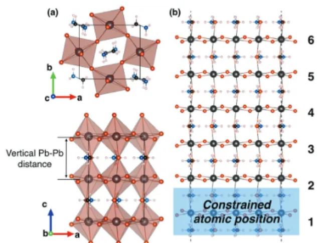
slab contains six PbBr6octahedra along the c-axis. During structure
optimization, the lattice parameters are fixed and the bottom octahedron (layer 1 in Fig. 1b) is kept frozen in the bulk configu-ration, while the rest of the structure is allowed to relax.
3 Results and discussion
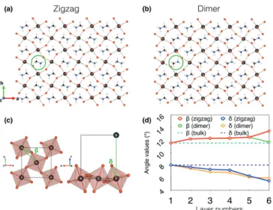
3.1 (001) surface reconstructions
The relaxation of the atomic positions at the (001) surface leads to two different reconstructions namely the zigzag and dimer phases (Fig. 2a and b). In the so-called zigzag phase, MA cations are organized in a way similar to the bulk structure, i.e. the organic molecules are oriented in a non-parallel manner. On the other hand, the dimer phase is obtained as a result of the in-plane rotation of half of MA cations on the top layer (layer 6) followed by the full optimization of atomic positions leading to a parallel configuration of MA cations corresponding to a rotation angle of B261. The dimer phase is 350 meV per supercell higher in energy than the zigzag phase, which amounts to 7.3 meV per MAPbBr3unit. This value compares
well with the energetic cost corresponding to the rotation of MA cations in MAPbI3.37 The zigzag phase would therefore be the
dominant one, however, the energy difference does not preclude the coexistence of both phases, as observed experimentally.27As
expected, the in-plane Pb–Br bonds show no significant sign of elongation or contraction, as compared to those of the frozen layer 1 in the bulk configuration (Table S1, ESI†). The same is observed for the out-of-plane Pb–Br bonds and the vertical Pb–Pb distances, except for the top layer that undergoes elongations of 0.05 Å and B0.10 Å, respectively, indicative of sizable surface breathing. Thus, the PbBr6 unit preserves its quasi-octahedral geometry
except for the top layer that shows stretching in the (001) direction.
Fig. 1 Bulk and surface structures of MAPbBr3. (a) View along (001) and
(010) of the bulk structure of the orthorhombic MAPbBr3in the Pnma
space group. (b) Slab of MAPbBr3having a (001) surface, terminated by Br
atoms and MA cations, used to inspect surface reconstruction. Layers are labelled 1–6 from the bulk to the surface.
Paper PCCP
Published on 08 March 2018. Downloaded by Bibliotheque de L’Universite de Rennes I on 22/05/2018 11:31:03.
Moreover, the corner-shared structure of halide perovskites provides additional degrees of freedom, namely for distortions which can be quantified by two characteristic angles: the in-plane (b) and out-of-in-plane (d) octahedron tilts (Fig. 2c).38Fig. 2d
shows the evolution of b and d on going from the bulk to the surface. Unlike the bond lengths where little variations are observed between the bulk and surface layers, the octahedron tilt angles undergo significant changes. For both the zigzag and dimer phases, d decreases progressively from the bulk to the surface (Table S1, ESI†). Noteworthily, surface octahedra show the lowest d tilt angles and are similar in the zigzag and dimer phases. This is not the case for the in-plane tilting b. In particular, b of the top layer remains close to the bulk value in the dimer phase, whereas b increases from B11.51 in the bulk to B13.51 on the surface of the zigzag phase. A direct consequence of this contrast is that Br–Br distances largely differ between the two phases (Fig. 3). Indeed, in the case of the zigzag case, all Br–Br distances at the surface maintain the same trend as in the relaxed bulk, although the values are
enlarged due to the surface effect. Meanwhile, because of the MA rotations, the dimer phase shows an alternation between short (B5.14 Å) and large (B6.49 Å) distances (Fig. 3b and c). This distinctive behaviour between the zigzag and dimer phases is at the origin of the striking differences observed in the recorded STM images.27
3.2 Electronic structure
Bulk MAPbBr3 retains the major features of the well-known
MAPbI3halide perovskite. Typically, the electronic band
struc-ture of the orthorhombic phase presents a direct band gap at G with a DFT energy band gap (including SOC) of about 1.1 eV.14
The highest valence states mainly arise from Br(4p) and Pb(6s) orbitals with anti-bonding hybridization, whereas the lowest conduction bands mainly originate from Pb(6p) orbitals (Fig. S3, ESI†). When moving from the bulk to the surface, the gap seemingly remains direct at G for both the zigzag and dimer phases (Fig. 4a and b, respectively). As a result of performing slab calculations to emulate the (001) surface and
Fig. 2 (001) surface reconstructions of MAPbBr3characterized by the rotation of MA cations. (a) (001) surface in the zigzag phase. (b) Same for the dimer
phase. (c) Definition of the in-plane, b, and out-of-plane, d, octahedron tilt angles. (d) Variation of the average tilt angles b and d from the bulk (layer 1) to the surface (layer 6, Table S1, ESI†).
Fig. 3 Bond-lengths of inequivalent Br–Br distances (Å) at the surface for (a) the bulk, (b) the zigzag phase, and (c) the dimer phase. Dotted lines indicate the limit of the unit cell.
This journal is © the Owner Societies 2018 Phys. Chem. Chem. Phys., 2018, 20, 9638--9643 | 9641
despite the 6-octahedron thickness of the slab, the system still experiences quantum confinement leading to a band gap open-ing that now amounts to 1.2 eV. Noteworthily, this is consistent with the experimental band structure obtained by ARPES.25
A direct consequence of surface relaxation is the localization of valence and conduction band densities.39In order to
illus-trate this point, we calculate the local density of states (LDOS) at the valence band maximum (VBM) and the conduction band minimum (CBM) for the zigzag (Fig. 4c) and dimer phases (Fig. S3, ESI†). The main features of the bulk are preserved: VBMs exhibit contributions from Br(4p) and Pb(6s) orbitals, and CBMs from Pb(6p) ones. However, in the relaxed struc-tures, the contribution of the VBM decreases at the surface and shifts toward the inner bulk layers, while the CBM gains significant weight on the surface. Importantly, this leads to the creation of a surface dipole reaching !7.2 Debye for the zigzag phase and !6.6 Debye for the dimer phase (the dipole is vanishing prior to surface relaxation). Interestingly, no remark-able difference between the LDOS of the zigzag and dimer phases can be noticed. Thus, the specific configuration of the MA molecules on the top of the surface is found to have little influence on neither charge densities at the band edges, band dispersions nor band gaps.
3.3 Rashba effect
A closer look at the band structures reveals that the VBMs (resp. CBMs) are split when SOC is included resulting in a shift of maxima (resp. minima) of energy away from G (Fig. 5a and b). Such a splitting is characteristic of the Rashba–Desselhaus effect.15,17The latter is a consequence of the combined effect
of a giant SOC and the loss of inversion symmetry caused by surface structural relaxation. It has been first described in zinc-blende semiconductors and wurtzite structures and later gen-eralized to quasi-2-dimensional systems.15–17Since it has been
characterized in semiconductor heterostructures,40bulks with
layered structures41or heavy atom surfaces.42Its amplitude is
quantified by a parameter a defined as a = 2E0/k0, where E0
is the splitting energy and k0 the momentum shift of the
maximum or the minimum of energy away from the high symmetry point (Fig. 5b). The calculated Rashba parameters a
for the zigzag and dimer phases are computed to be 0.59 eV Å (0.24 eV Å) and 0.44 eV Å (0.27 eV Å) for the CBM (VBM), respectively (Table 1). These calculated values are more than one order of magnitude smaller than the values (7 " 1 eV Å for the VBM) extracted from ARPES experiments performed over cleaved single crystals of MAPbBr3.26Moreover, given the small
difference computed between the zigzag and dimer phases, one can hardly explain these experimental values on the basis of simple surface reconstructions associated with the flip of half of surface MA molecules. Among possible interpretations, it
Fig. 4 Electronic properties of the reconstructed surfaces. Electronic band structures including SOC for the relaxed (a) zigzag and (b) dimer phases. The direct band gap amounts to 1.2 eV for both phases. (c) LDOS of the VBM and the CBM for the relaxed zigzag phase (see Fig. S4, ESI† for the dimer phase).
Fig. 5 Rashba effect in the reconstructed surfaces. (a) Electronic band structure of the zigzag phase with (straight lines) and without (dashed lines) SOC. (b) Zoom in the dispersions of the VBM and the CBM revealing the Rashba spinor splitting for each of the two reconstructed phases. Defini-tion of E0and k0, respectively, the energy splitting and momentum shift,
needed to define the Rashba parameter a = 2E0/k0is also shown.
Table 1 The Rashba parameter a for both phases are calculated using the following expression: a = 2E0/k0. E0represents the splitting energy and k0
the momentum shift of the maximum or the minimum of energy away from the high symmetry point
Slabs E0(10!4) (eV) k0(Å) a (eV Å) Zigzag CBM 8.00 0.0027 0.59
VBM 1.32 0.0011 0.24 Dimer CBM 12.00 0.0055 0.44 VBM 2.84 0.0021 0.27
Paper PCCP
Published on 08 March 2018. Downloaded by Bibliotheque de L’Universite de Rennes I on 2/15/2021 4:17:34 PM.
could be associated with larger polar surface reconstructions and the creation of mesoscale ferroelectric domains.43Indeed,
the beams used in ARPES cover surface areas that are much larger than the ones considered in the present DFT study. Unfortunately, such large supercell simulations are beyond available computational resources. Alternatively, despite the careful use of freshly cleaved surfaces,26,44the discrepancy of
the results could originate from the presence of defects at the crystal surface in the experimental setup. As Rashba splitting is very sensitive to the local symmetry, the presence of defects could lead to large values of a escaping our description of a flawless surface. Other fascinating experimental results have been reported for surface-dependent optoelectronic properties of the halide perovskites and especially MAPbBr3. There is
indeed a strong interplay between ultravacuum conditions and the chemistry of the surface.45Moreover, our findings of
noticeably smaller Rashba splitting is also supported by the second set of ARPES experiments performed over single crystals of MAPbBr3by another group,25which makes no mention of
Rashba splitting, indicating that if any it is below their experi-mental resolution.
4 Conclusion
In summary, we investigated the (001) surface of the low-temperature orthorhombic phase of MAPbBr3 and the effect
of surface relaxation on the electronic properties. In agreement with recent STM experiments, we inspected two 2 ! 2 (001) nanoscale surface reconstructions considering zigzag and dimer phases, which are characterized by different orientations of MA cations at the surface. First, for both phases surface reconstruction leads to sizeable elongation of the surface Pb–Pb bond lengths whereas the bottom layers remain similar to the bulk structure. Concomitantly, the surface in-plane octahedron tilt angles increase whereas the out-of-plane tilt angles decrease. Except for a slight increase of the band gap as a result of quantum confinement related to the finite and limited thickness of the slabs, the overall band structure remains similar to that computed for the bulk. Interestingly, the valence and conduction band densities reveal different spatial localizations, with the former pushing towards the bulk whereas the later gaining significantly more weight on the surface octahedra. Besides, a detailed inspec-tion of the valence and conducinspec-tion band dispersions of the reconstructed surface reveals the existence of the Rashba effect, both in valence and conduction bands, as a result of inversion symmetry breaking in the presence of strong spin–orbit coupling. However, the computed spinor splittings are more than an order of magnitude smaller than those experimentally reported for MAPbBr3,26indicating that these experimental observations
can-not be traced back to the atomic scale 2 ! 2 surface reconstruction considered in our study. Thus such huge Rashba parameters are either related to mesoscale polar reconstructions, which do no correspond to the local ones evidenced by STM,27 or to the
presence of defects at the surface of the MAPbBr3single crystal.
The examination of punctual defects, e.g. vacancies, as well as step-edges will be carried out in the future.
Conflicts of interest
There are no conflicts to declare.
Acknowledgements
The work at Institut des Sciences Chimiques de Rennes and Institut FOTON was supported by Agence National pour la Recherche (SuperSansPlomb and TRANSHYPERO projects). This work was granted access to the HPC resources of [TGCC/ CINES/IDRIS] under the allocation 2017-A0010907682 made by GENCI.
References
1 A. Kojima, K. Teshima, Y. Shirai and T. Miyasaka, J. Am. Chem. Soc., 2009, 131, 6050–6051.
2 NREL chart, https://www.nrel.gov/pv/assets/images/efficiency-chart.png.
3 W. S. Yang, B.-W. Park, E. H. Jung, N. J. Jeon, Y. C. Kim, D. U. Lee, S. S. Shin, J. Seo, E. K. Kim, J. H. Noh and S. I. Seok, Science, 2017, 356, 1376–1379.
4 M. A. Green, Prog. Photovoltaics Res. Appl., 2011, 20, 472. 5 K.-H. Lee, K. Araki, L. Wang, N. Kojima, Y. Ohshita and
M. Yamaguchi, Prog. Photovoltaics Res. Appl., 2016, 24, 1310. 6 E. M. Sanehira, A. R. Marshall, J. A. Christians, S. P. Harvey, P. N. Ciesielski, L. M. Wheeler, P. Schulz, L. Y. Lin, M. C. Beard and J. M. Luther, Sci. Adv., 2017, 3, eaao4204. 7 C. C. Stoumpos, C. D. Maliakas and M. G. Kanatzidis, Inorg.
Chem., 2013, 52, 2013.
8 K. Tvingstedt, O. Malinkiewicz, A. Baumann, C. Deibel, H. J. Snaith, V. Dyakonov and H. J. Bolink, Sci. Rep., 2014, 4, 6071.
9 Y. Yamada, T. Nakamura, M. Endo, A. Wakamiya and Y. Kanemitsu, IEEE J. Photovolt., 2015, 5, 401.
10 H. Huang, L. Polavarapu, J. A. Sichert, A. S. Susha, A. S. Urban and A. L. Rogach, NPG Asia Mater., 2016, 8, e328. 11 J. Even, L. Pedesseau, M.-A. Dupertuis, J.-M. Jancu and C. Katan, Phys. Rev. B: Condens. Matter Mater. Phys., 2012, 86, 205301.
12 J. Even, L. Pedesseau, J.-M. Jancu and C. Katan, J. Phys. Chem. Lett., 2013, 4, 2999.
13 J. Even, L. Pedesseau, J.-M. Jancu and C. Katan, Phys. Status Solidi RRL, 2014, 8, 31–35.
14 C. Katan, L. Pedesseau, M. Kepenekian, A. Rolland and J. Even, J. Mater. Chem. A, 2015, 3, 9232–9240.
15 G. Dresselhaus, Phys. Rev., 1955, 100, 580.
16 Y. A. Bychkov and E. I. Rashba, J. Exp. Theor. Phys., 1984, 39, 78.
17 E. I. Rashba, Phys. Solid State, 1960, 2, 1224.
18 M. Kim, J. Im, A. J. Freeman, J. Ihm and H. Jin, Proc. Natl. Acad. Sci. U. S. A., 2014, 111, 6900.
This journal is © the Owner Societies 2018 Phys. Chem. Chem. Phys., 2018, 20, 9638--9643 | 9643
19 F. Brivio, K. T. Butler and A. Walsh, Phys. Rev. B: Condens. Matter Mater. Phys., 2014, 89, 155204.
20 A. Amat, E. Mosconi, E. Ronca, E. Quarti, P. Umari, M. K. Nazeeruddin, M. Gra¨tzel and F. D. Angelis, Nano Lett., 2014, 14, 3608–3616.
21 A. Stroppa, D. Di Sante, P. Barone, M. Bokdam, G. Kresse, C. Franchini, M. H. Whangbo and S. Picozzi, Nat. Commun., 2014, 5, 5900.
22 M. Kepenekian, R. Robles, C. Katan, D. Sapori, L. Pedesseau and J. Even, ACS Nano, 2015, 9, 11557.
23 E. Mosconi, T. Etienne and F. De Angelis, J. Phys. Chem. Lett., 2017, 8, 2247.
24 M. Kepenekian and J. Even, J. Phys. Chem. Lett., 2017, 8, 3362–3370.
25 T. Komesu, X. Huang, T. R. Paudel, Y. B. Losovyj, X. Zhang, E. F. Schwier, Y. Kojima, M. Zheng, H. Iwasawa, K. Shimada, M. I. Saidamisov, D. Shi, A. L. Abdelhady, O. M. Bakr, S. Dong, E. Y. Tsymbal and P. A. Dowben, J. Phys. Chem. C, 2016, 120, 21710.
26 D. Niesner, M. Wilhelm, I. Levchuk, A. Osvet, S. Shrestha, M. Batentschuk, C. Brabec and T. Fauster, Phys. Rev. Lett., 2016, 117, 126401.
27 R. Ohmann, L. K. Ono, H.-S. Kim, H. Lin, M. V. Lee, Y. Li, N.-G. Park and Y. Qi, J. Am. Chem. Soc., 2015, 137, 16049. 28 P. Hohenberg and W. Kohn, Phys. Rev., 1964, 136,
B864–B871.
29 W. Kohn and L. J. Sham, Phys. Rev., 1965, 140, A1133–A1138. 30 J. M. Soler, E. Artacho, J. D. Gale, A. Garcı´a, J. Junquera, P. Ordejo´n and D. Sa´nchez-Portal, J. Phys.: Condens. Matter, 2002, 14, 2745–2779.
31 V. R. Cooper, Phys. Rev. B: Condens. Matter Mater. Phys., 2009, 81, 161104.
32 N. Troullier and J. L. Martins, Phys. Rev. B: Condens. Matter Mater. Phys., 1991, 43, 1993.
33 D. Sa´nchez-Portal, E. Artacho, P. Ordejo´n, A. Garcı´a and J. M. Soler, Phys. Status Solidi, 1999, 215, 809.
34 L. Bengtsson, Phys. Rev. B: Condens. Matter Mater. Phys., 1999, 59, 12301–12304.
35 I. P. Swainson, R. Hammond, C. Soullie`re, O. Knop and W. Massa, J. Solid State Chem., 2003, 176, 97.
36 L. She, M. Liu and D. Zhong, ACS Nano, 2015, 10, 1126–1131.
37 Y. Li, M. Behtash, J. Wong and K. Yang, J. Phys. Chem. C, 2018, 122, 177–184.
38 L. Pedesseau, D. Sapori, B. Traore, R. Robles, H. H. Fang, M.-A. Loi, H. Tsai, W. Nie, J.-C. Blancon, A. J. Neukirch, S. Tretiak, A. D. Mohite, C. Katan, J. Even and M. Kepenekian, ACS Nano, 2016, 10, 9776.
39 M. Kepenekian, B. Traore, J.-C. Blancon, L. Pedesseau, H. Tsai, W. Nie, C. C. Stoumpos, M. G. Kanatzidis, J. Even, A. D. Mohite, S. Tretiak and C. Katan, 2018, arXiv: 1801.00704. 40 J. Nitta, T. Akazaki, H. Takayanagi and T. Enoki, Phys. Rev.
Lett., 1997, 78, 1335.
41 K. Ishizaka, M. Bahramy, H. Murakawa, M. Sakano, T. Shimojima, T. Sonobe, K. Koizumi, S. Shin, H. Miyahara, A. Kuimura, K. Miyamoto, T. Okuda, H. Namatame, M. Taniguchi, R. Arita, N. Nagaosa, K. Kobayashi, Y. Murakami, R. Kumai, Y. Kaneko, Y. Onose and Y. Tokura, Nat. Mater., 2011, 10, 521. 42 S. LaShell, B. A. McDougall and E. Jensen, Phys. Rev. Lett.,
1996, 77, 3419.
43 Y. Kutes, L. Ye, Y. Zhou, S. Pang, B. D. Huey and N. P. Padture, J. Phys. Chem. Lett., 2014, 5, 3335.
44 D. Niesner, O. Schuster, M. Wilhelm, I. Levchuk, A. Osvet, S. Shrestha, M. Batentschuk, C. Brabec and T. Fauster, Phys. Rev. B: Condens. Matter Mater. Phys., 2017, 95, 075207. 45 H.-H. Fang, S. Adjokatse, H. Wei, J. Yang, G. R. Blake,
J. Huang, J. Even and M.-A. Loi, Sci. Adv., 2016, 2, e1600534.
Paper PCCP
Published on 08 March 2018. Downloaded by Bibliotheque de L’Universite de Rennes I on 2/15/2021 4:17:34 PM.