HAL Id: hal-01891887
https://hal.archives-ouvertes.fr/hal-01891887
Submitted on 10 Oct 2018
HAL is a multi-disciplinary open access
archive for the deposit and dissemination of
sci-entific research documents, whether they are
pub-lished or not. The documents may come from
teaching and research institutions in France or
abroad, or from public or private research centers.
L’archive ouverte pluridisciplinaire HAL, est
destinée au dépôt et à la diffusion de documents
scientifiques de niveau recherche, publiés ou non,
émanant des établissements d’enseignement et de
recherche français ou étrangers, des laboratoires
publics ou privés.
Optimization of porous silicon waveguide design for
micro-ring resonator sensing applications
Paul Azuelos, Pauline Girault, Nathalie Lorrain, Yannick Dumeige, Loïc
Bodiou, Luiz Poffo, Mohammed Guendouz, Monique Thual, Joel Charrier
To cite this version:
Paul Azuelos, Pauline Girault, Nathalie Lorrain, Yannick Dumeige, Loïc Bodiou, et al.. Optimization
of porous silicon waveguide design for micro-ring resonator sensing applications. Journal of Optics,
Institute of Physics (IOP), 2018, 20 (8), pp.085301. �10.1088/2040-8986/aad01b�. �hal-01891887�
1
Optimization of porous silicon waveguide design for micro-ring resonator
sensing applications
Authors: Paul Azuelosa*, Pauline Giraulta, Nathalie Lorraina, Yannick Dumeigea, Loïc Bodioua, Luiz Poffoa,
Mohammed Guendouza, Monique Thuala and Joël Charriera
a Univ Rennes, CNRS, Institut FOTON – UMR 6082, F-22305, Lannion, France
* Corresponding author: [email protected]
Abstract:
The design of Porous Silicon (PSi) integrated micro-resonators is studied for both surface sensing and homogeneous sensing at 1550 nm to optimize the sensors’ sensitivity and Limit of Detection (LOD) as a function of the porosity, dimensions and propagation losses of PSi ridge waveguides. A model for estimating the different contributions to the losses of PSi waveguide as a function of the dimensions and the porosity is then developed to allow calculation of the performance of the sensor. Low refractive index difference and high porosities mean that higher sensor performance can be obtained due to the reduction of surface scattering losses as the waveguide dimensions become larger.
The sensitivity and limit of detection calculated in this paper for optimized dimensions and porosities of PSi ridge waveguides are respectively 0.04 nm/(pg.mm-2) and 0.5 pg.mm-2 for Bovin Serum Albumin (BSA)
molecules surface sensing which are higher than the state of the art.
For homogeneous detection, a promising sensitivity of 800 nm/RIU, higher than the sensitivities that can be currently obtained with one micro-resonator, has been estimated. A limit of detection of 1.2.10-4 RIU, which is
within the range of state of the art of micro-resonator (MR) based biological sensors, has also been calculated for homogeneous detection. These promising results obtained by the optimization of the porosity and the ridge waveguide dimensions with respect to optical losses reinforce the attraction of PSi for integrated optical sensing application.
Highlights:
- The performances of micro-ring resonator biological sensor based on porous silicon waveguides are calculated in terms of sensitivity and limit of detection as a function of porosity and waveguide dimensions.
- A micro-resonator is designed for both surface and homogeneous sensing by taking into account the optical losses.
- A comparison of the performances of micro-resonator sensors for both surface and homogenous detection highlights the interest of porous silicon waveguides having optimized porosities and dimensions, in obtaining the best limit of detection and sensitivity that are currently possible to reach with only one micro-resonator.
Keywords: Porous silicon, Micro-resonator, Optical integrated sensor, optical losses calculation, 1. Introduction
The development of sensors to detect various molecules including gas, proteins or viruses has an important role in societal applications such as food safety, environmental monitoring, health and defense.
Such sensors must provide a fast, sensitive and selective detection response with a low limit of detection (LOD). Among the existing integrated transducers, different optical devices such as evanescent waveguides [1], slot waveguides [2, 3], Mach-Zehnder interferometers [4, 5], photonic crystals [6, 7], and micro-resonators [8, 9] have been developed.
Integrated micro-resonators (MRs) have been successfully used for biosensor applications with high sensitivity and low LOD. Most of these MR sensors are based on evanescent wave detection. The Electromagnetic field (EM-field) guided in the waveguide can directly interact with analytes which are grafted onto the surface of a functionalized MR [10, 11]. In this case the interaction is called “surface sensing”. On the other hand “homogeneous sensing”, occurs when the guided EM-field interacts with the analytes in the surrounding medium
2
(superstrate). Both types of interaction lead to a wavelength shift in the MR response due to the variation of the superstrate refractive index induced by the presence of analytes.
A LOD of 17 pg.mm-2 has been achieved with SOI MRs [12] for Avidin molecule surface detection
whereas a sensitivity of 200 nm/RIU (Refractive Index Unit) [13] for a polymer MR sensor and a LOD of 7. 6.10 -7 RIU [11] for a SOI MR sensor has been obtained for homogeneous sensing.
To improve the sensor performance, the interaction between the propagated light and the analytes can be further enhanced using a porous material such as porous silicon (PSi) for the MR waveguide. PSi layer is a three dimensional porous material which optimizes molecules interactions with the guided EM-field and increases the binding sites for surface functionalization because of its high specific internal surface [14].
PSi is also interesting because of its tunable porosity which varies with the fabrication parameters. This adjustable porosity, directly related to its refractive index (which can then vary between the air index and that of bulk silicon), allows the fabrication of waveguides [15]. An oxidation step is, however, necessary to reduce its hydrophobicity and instability [18].
In addition, PSi is already widely used as an active detection layer for biomolecules because of its biocompatibility which allows easier functionalization [16].
Moreover, the potential of PSi as a material for the implementation of MRs destined for sensor applications has been demonstrated by Hutter et al. [17] giving an improvement of sensitivity, which can theoretically achieve 700 nm/RIU . The creation of the first PSi based MR sensor was demonstrated by [18] with a sensitivity of 380 nm/RIU for homogeneous sensing of salt. Very recently, our group obtained a sensitivity of 560 nm/RIU for homogeneous sensing of glucose with single ridge PSi MR fabricated using a standard photolithography process and a LOD of 8.10-5 RIU, equivalent to a glucose concentration of 0.7 g/L, has been
achieved [19].
One possibility to further greatly increase the sensitivity of the ridge PSi based MR sensor is to make use of the tunability of the porosity and dimensions of the waveguide.
In this paper, therefore, a general method is presented in order to optimize the sensitivity and the LOD of PSi MR integrated transducers for both surface sensing and homogeneous sensing at 1550 nm by considering the porosity and the dimensions of PSi ridge waveguides. The different contributions of the propagation losses are also taken into consideration as they constitute an important parameter in regards of the LOD value. So optical losses and mode field profiles for PSi based ridge waveguides are estimated in order to calculate the theoretical LOD for both surface and homogeneous sensing. This general method can be applied to other porous materials for both surface and homogeneous sensing. After a review of the principle of a sensor based on a MR, the definition of sensitivity and LOD are given for the two types of detection. Then, the oxidation rate, the porosity and the refractive index of PSi layers used to fabricate the waveguides are presented. Two ridge waveguides of different sizes and refractive indices are studied for the simulations. The different contributions of the propagation losses such as, surface scattering losses, volume diffusion losses and material absorption losses are defined and estimated for different configurations. Finally, the results of the sensitivity and LOD calculations are discussed in order to outline an approach which gives a way of reaching highly sensitive PSi MR sensors with a low LOD.
2. Introduction to micro-resonator sensors for sensing application
The MR studied, presented in Fig.1a, is a single side coupled micro-racetrack defined by a radius R and a coupling length Lc separated by a gap g from an access waveguide.
3
Figure.1.a) Diagram of a single side coupled micro-racetrack resonator. The field amplitudes are denoted by Ei
(incident) and Et (transmitted). Self-coupling (τ) and cross-coupling (κ) amplitude coefficients are also indicated.
b) Transmission spectrum of a single side coupled micro-racetrack resonator in the presence (red) or absence (green) of analytes.
The light is coupled into the cavity by evanescent coupling and the cross-coupling amplitude κ between the access waveguide and the resonant cavity can be calculated with the analytical methods presented in [20]. By setting the different following parameters and constants:
- L is the perimeter of the MR,
- a is the attenuation coefficient per MR round trip which is linked to 𝛼𝑜𝑣𝑒𝑟𝑎𝑙𝑙 which represents the MR optical propagation losses,
- 𝛽 =2𝜋
𝜆 . 𝑛𝑒𝑓𝑓 is the MR propagation constant,
- 𝜂 is the coupling efficiency coefficient between the access and MR waveguides. In this study, a symmetrical lossless coupling is assumed, so 𝜂=1 and |𝜏|2+ |𝜅|2= 1,
the MR intensity transmission is given by the following equation:
𝑇(𝜆) = |𝐸𝑡 𝐸𝑖| 2 = |𝜂. 𝜏 − 𝜂. a. exp(𝑗𝜙) 1 − τ. 𝜂. a. exp(𝑗𝜙)| 2 (1) with 𝜙 = 𝐿. 𝛽 L = 2πR + 2L𝐶 (2) and 𝜏 = √1 − 𝜅2 (3) and a = 𝜂. exp(−𝐿.𝛼𝑜𝑣𝑒𝑟𝑎𝑙𝑙 2 ) (4)
At the output of the access waveguide, periodic resonance occurs in the transmission spectrum at res according to
the following condition:
𝜆𝑟𝑒𝑠 =
2𝜋𝐿𝑛𝑒𝑓𝑓 𝑝
(5)
with p an integer parameter and neff the effective index of the propagated mode.
The Full Width at Half Maximum (FWHM) of the resonance is estimated for a MR with the analytical expression given by [21]: 𝐹𝑊𝐻𝑀(𝑛𝑚) = 𝜆𝑟𝑒𝑠 2 𝜋. 𝐿. 𝑛𝑒𝑓𝑓 × (1 |𝜏|. 𝑒 −𝛼𝑜𝑣𝑒𝑟𝑎𝑙𝑙.𝐿 2− |𝜏|𝑒𝛼𝑜𝑣𝑒𝑟𝑎𝑙𝑙.𝐿2) (6)
The main experimental technique (Fig.1.b) used to detect the presence of analytes with a MR is based on the resonance wavelength shift of the transmission spectrum. This consists of measuring the spectral shift of the
4
resonance peak 𝜆𝑟𝑒𝑠 due to the presence of analytes. Thus, the shift in the resonance peak Δλres of the MR
transmission is induced by the refractive index variation due to the presence of analytes.
An integrated MR relies on this variation of the effective index 𝑛𝑒𝑓𝑓 to detect the presence of grafted analytes for surface sensing or solubilized analytes for homogeneous sensing as described in Fig.2.
Figure.2.a) Surface sensing applicationb) Homogeneous sensing application.
To optimize the MR sensitivity, the variation of 𝑛𝑒𝑓𝑓 with the analyte concentration must be as high as possible. So therefore, the interaction between the propagated light and the analytes should be increased. In this work, PSi is used for fabricating the MR waveguides (see Fig.2.a). PSi waveguides can be used for both surface and homogeneous sensing. When used for surface sensing, the high specific surface of PSi, up to 500 m2.cm-3 for
mesoporous silicon, increases the interaction between EM-field and analytes grafted onto the functionalized surface [22]. Surface sensing experiment can be carried out with an air superstrate as the analytes are grafted to the internal surface after surface functionalization and drying steps. For homogeneous sensing (see Fig.2.b), the interaction between the EM-field and analytes is enhanced as the analyte in solution infiltrates the pores of the guiding layer.
Surface sensitivity Ssurf. depends on the variation of the effective index of the propagated mode, taking
into account the variation of the analytes mass per unit of surface grafted onto the waveguide silicon crystallite surface (Fig.2.a). Ssurf. is defined as:
𝑆𝑠𝑢𝑟𝑓.(𝑛𝑚 (𝑝𝑔. 𝑚𝑚⁄ −2)) = 𝜕𝜆 𝜕𝑛𝑒𝑓𝑓 𝜕𝑛𝑒𝑓𝑓 𝜕𝑀𝑎𝑛𝑎𝑙𝑦𝑡𝑒𝑠 = 𝜆𝑟𝑒𝑠 𝑛𝑔(𝜆) 𝜕𝑛𝑒𝑓𝑓 𝜕𝑀𝑎𝑛𝑎𝑙𝑦𝑡𝑒𝑠 (7)
With 𝑀𝑎𝑛𝑎𝑙𝑦𝑡𝑒𝑠 the mass of target molecules grafted inside the waveguide per unit of surface and with ng the group
index.
The quantity of analytes grafted on the surface of the porous silicon waveguide can be calculated with the model developed by J.Charrier et al. [23]. As the quantity of analytes grafted on the surface of the waveguides depends on its properties, the Bovin Serum Albumin molecule (BSA) studied in [23] is taken as a reference analyte for surface sensing in this paper. The calculation of the sensitivity can be adapted to other analytes by evaluating the variation of effective index as a function of the mass concentration of grafted analytes.
Homogeneous sensitivity Shom. depends on the variation of the effective index of propagated mode as a
function of the variation of the refractive index variation of the aqueous solution infiltrated in the pores of the guiding layer (Fig.2.b). In a similar way to surface sensitivity 𝑆ℎ𝑜𝑚 can be expressed as:
5
𝑆ℎ𝑜𝑚.(𝑛𝑚 𝑅𝐼𝑈⁄ ) = 𝜕𝜆 𝜕𝑛𝑒𝑓𝑓 𝜕𝑛𝑒𝑓𝑓 𝜕𝑛𝑐 = 𝜆𝑟𝑒𝑠 𝑛𝑔(𝜆) 𝜕𝑛𝑒𝑓𝑓 𝜕𝑛𝑐 (8)with nc the refractive index of the detection medium (guiding layer) and ng the group index.
The refractive index of the porous silicon layers can be estimated with the Bruggeman model [24],[25]. The effective index of the propagated mode and the group index can then be calculated.
The LOD is the minimum quantity of analytes detectable by the sensor. It is expressed in (pg.mm-2) or in
(RIU) for surface and homogeneous detection respectively. LOD can be estimated by [26]
𝐿𝑂𝐷(𝑝𝑔. 𝑚𝑚−2𝑜𝑟𝑅𝐼𝑈) =3𝜎 𝑆
(9)
with 𝜎 the total system noise variance defined by:
𝜎 = √𝜎𝑎𝑚𝑝𝑙−𝑛𝑜𝑖𝑠𝑒2 + 𝜎
𝑡𝑒𝑚𝑝−𝑖𝑛𝑑𝑢𝑐𝑒2 + 𝜎𝑠𝑝𝑒𝑐𝑡−𝑟𝑒𝑠2
(10)
where: 𝜎𝑎𝑚𝑝𝑙−𝑛𝑜𝑖𝑠𝑒, 𝜎𝑡𝑒𝑚𝑝−𝑖𝑛𝑑𝑢𝑐𝑒 and 𝜎𝑠𝑝𝑒𝑐𝑡−𝑟𝑒𝑠 are the noise related to intensity fluctuations, the temperature induced and the spectral resolution standard deviation respectively :
- The parameters 𝜎𝑡𝑒𝑚𝑝−𝑖𝑛𝑑𝑢𝑐𝑒 and 𝜎𝑠𝑝𝑒𝑐𝑡−𝑟𝑒𝑠 are fixed by the experimental setup.
- 𝜎𝑠𝑝𝑒𝑐𝑡−𝑟𝑒𝑠 standard deviation can be set to 0.29pm corresponding to a 1 pm resolution spectrum analyzer commonly used for sensing experiment [20], the temperature induced standard deviation can be neglected assuming a thermally stabilized setup 𝜎𝑡𝑒𝑚𝑝−𝑖𝑛𝑑𝑢𝑐𝑒≪ (𝜎𝑠𝑝𝑒𝑐𝑡−𝑟𝑒𝑠, 𝜎𝑎𝑚𝑝𝑙−𝑛𝑜𝑖𝑠𝑒) [27].
- 𝜎𝑎𝑚𝑝𝑙−𝑛𝑜𝑖𝑠𝑒 can be calculated from the Full Width at Half Maximum (FWHM) of the resonance peak of the MR transmission given by equation (6) and the setup Signal to Noise Ratio (SNR) given by [26]; Standard integrated optics experimental setup SNR with porous silicon MR is estimated to 40 dB in this paper.
𝜎𝑎𝑚𝑝𝑙−𝑛𝑜𝑖𝑠𝑒=
𝐹𝑊𝐻𝑀 4.5(𝑆𝑁𝑅0.25)
(11)
To estimate the LOD, the FWHM value can be deduced from the transmission response of a reference MR with a radius R=100 µm, with given optical losses per MR round trip (parameter a defined in equation (4)) that will have to be estimated for the configuration of critical coupling which ensures a maximal contrast.
3. Porous silicon waveguide for sensing applications
The principal parameters of the sensor (LOD and sensitivity) have been defined by using a micro-racetrack resonator as transducer. The fabrication of the transducer based on PSi layers is described in the next sections and the optical losses will be estimated for different detection configurations by using an aqueous medium (for homogenous detection) or an air medium (for surface detection) as the superstrate.
3.1 Porous silicon fabrication: porosity, oxidation rate and refractive index
PSi is formed by electro-chemical anodization etching of a silicon substrate using a hydrofluoric acid solution. The porosity of the material is controlled by the etching parameters such as current density or electro-chemical solution composition. After this, an oxidation step of the PSi layers at 500°C has to be carried out in order to stabilize the pores and to decrease the native hydrophobicity of PSi layers. This is necessary to allow either functionalization and analyte grafting for surface sensing or aqueous solution penetration for homogeneous sensing. This thermal step at 500°C performed under air for one hour permits a partial oxidation of PSi layers with an oxidation rate (𝑡𝑜𝑥) near 30% estimated by [19] (fraction of oxidized silicon) that allows the retention of a high porosity layer, the oxidation step inducing a 𝑉𝑒𝑥𝑝 =27% volume expansion of the silicon crystallites.
6
The refractive index of the PSi layers has been determined after the partial oxidation step. For porous silicon, the refractive index has been calculated by the Bruggeman method which calculates the refractive index of effective material by taking into account the volume fraction of each component and its refractive index [28] :
𝑝 𝑛𝑎𝑖𝑟/𝑤𝑎𝑡𝑒𝑟 2− 𝑛2 𝑛𝑎𝑖𝑟/𝑤𝑎𝑡𝑒𝑟2+ 2𝑛2 + 𝑓𝑆𝑖,𝑜𝑥 𝑛𝑆𝑖2− 𝑛2 𝑛𝑆𝑖2+ 2𝑛2 + 𝑓𝑆𝑖𝑂2 𝑛𝑆𝑖𝑂2 2− 𝑛2 𝑛𝑆𝑖𝑂2 2+ 2𝑛2= 0 (12)
With p the porosity of the partially oxidized PSi and n the effective index of the PSi. 𝑛𝑆𝑖𝑂2, 𝑛𝑆𝑖 and 𝑛𝑎𝑖𝑟/𝑤𝑎𝑡𝑒𝑟 are
the refractive index of oxidized silicon, silicon and air or water. 𝑓𝑆𝑖,𝑜𝑥,𝑓𝑆𝑖,𝑖𝑛𝑖𝑡 and 𝑓𝑆𝑖𝑂2correspond respectively to the remaining volume fraction of Si after the oxidation, the initial volume fraction of Si before oxidation, the resulting volume fraction of SiO2 after the oxidation. These volume fractions are linked to 𝑡𝑜𝑥 , p and 𝑉𝑒𝑥𝑝 by the relations : { 𝑓𝑆𝑖,𝑜𝑥= 𝑓𝑆𝑖,𝑖𝑛𝑖𝑡(1 − 𝑡𝑜𝑥) 𝑝 = 𝑝𝑖𝑛𝑖𝑡− (1 + 𝑉𝑒𝑥𝑝)𝑡𝑜𝑥𝑓𝑆𝑖,𝑖𝑛𝑖𝑡 𝑡𝑜𝑥 =𝑓𝑆𝑖,𝑖𝑛𝑖𝑡+ 𝑓𝑆𝑖𝑂2 𝑓𝑆𝑖,𝑖𝑛𝑖𝑡 (13)
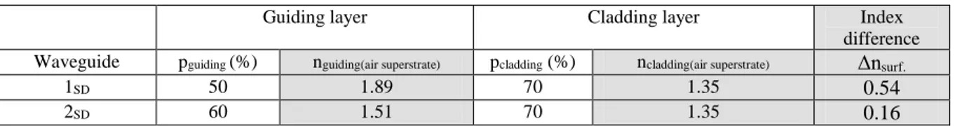
In the next sections, two waveguide configurations (1 and 2) which differ in the porosity of the guiding core layer are considered. The objective is to study the effect of refractive index difference between PSi cladding and guiding layers on waveguide dimensions required to obtain single mode waveguide, on the optical losses and finally on the sensitivity and LOD. The two configurations in terms of porosity, refractive index and difference in refractive index are presented in Table I for air superstrate in case of surface detection (1SD and 2SD) and in Table
II, for water superstrate (1HD and 2HD) for homogeneous detection.
Table I: Porosity and refractive index values at 1550 nm for the two types of waveguides studied for surface detection (in this case, the superstrate is air). n corresponds to the index difference between guiding and cladding layers.
Guiding layer Cladding layer Index
difference Waveguide pguiding (%) nguiding(air superstrate) pcladding (%) ncladding(air superstrate) Δnsurf.
1SD 50 1.89 70 1.35 0.54
2SD 60 1.51 70 1.35 0.16
Table II: Porosity and refractive index values at 1550 nm for the two types of waveguides studied for homogeneous detection (in this case, the superstrate is water). n corresponds to the index difference between guiding and cladding layers.
Guiding layer Cladding layer Index
difference Waveguide pguiding (%) nguiding(water superstrate) pcladding (%) ncladding(water superstrate) Δnhom.
1HD 50 2.03 70 1.57 0.46
2HD 60 1.70 70 1.57 0.13
The layer porosity values in Table I and II are carefully chosen to illustrate the principal trends in sensitivity and LOD for the two types of sensing applications. For aheavily-doped P Si substrate, the porosity p of the PSi, after the thermal oxidation step at 500°C, varies between 50% and 70% [18]. The cladding layer porosity has therefore been chosen as 70 %, which is the maximum porosity achievable for this configuration. The guiding layer porosity value has beenfixed to obtain an index difference between the guiding and the cladding layers close to Δn = 0.50 (configuration 1) or Δn = 0.15 (configuration 2) for homogeneous and surface detection respectively.
The porosity values of the different waveguides are the same in table I and II respectively for surface and homogeneous detection, but homogeneous detection implies the presence of water as the superstrate. Infiltration of water into the pores explains the higher refractive index of the porous layers in this case as compared to surface detection.
The effective index of the propagated mode has been calculated with a Finite Difference Method solver [29], from the refractive index of each waveguide configuration presented in Table I and II. The cladding and superstrate
7
layers have been taken thick enough to have no influence on the modal characteristics. Only the waveguide dimensions which allow single mode configuration will be considered here. The effective index of the single mode TE00 for surface detection and the two configurations presented in Table I are presented in Figure 3. For ease of
presentation, the geometrical dependence of losses, sensitivity and LOD will be presented on the same figure for the two configurations later in this paper.
Figure.3. a) Effective index of configuration 1 for surface detection for single mode condition TE00 and at 1550
nm b) Effective index of configuration 2 for surface detection for single mode condition TE00 and at 1550 nm
3.2 Study of porous silicon waveguides losses
PSi waveguides optical losses𝛼𝑜𝑣𝑒𝑟𝑎𝑙𝑙. depend on the surface scattering losses 𝛼𝑠𝑢𝑟𝑓_𝑠𝑐𝑎𝑡𝑒𝑟𝑟𝑖𝑛𝑔, the volume diffusion losses 𝛼𝑣𝑜𝑙_𝑑𝑖𝑓𝑓 and the material absorption 𝛼𝑎𝑏𝑠_𝑚𝑎𝑡[30]. For the micro-racetrack resonator, the high radius value (R=100 µm) is sufficiently large to allow neglect of the curvature losses.
In this section, each contribution to the losses in PSi ridge waveguides is calculated and presented for waveguide 2 configuration only, both for surface and homogeneous detection. The tendencies for configuration 1 are calculated similarly. Square section waveguides of two dimensions have been first considered to illustrate the effect of the waveguide dimensions on the contributions to the losses. At the end of the section, the overall losses are then presented for both configuration 1 and 2. The effect of the dimensions of the waveguide is generalized to rectangular section.
The surface scattering losses 𝛼𝑠𝑢𝑟𝑓_𝑠𝑐𝑎𝑡𝑒𝑟𝑟𝑖𝑛𝑔 induced by surface roughness has been calculated adapting the model developed by Payne et.al. [31] to ridge waveguides [32]. In Fig.4, surface scattering losses are plotted as a function of the surface roughness and for 2SD and 2HD ridge waveguides core dimensions of 1.5 x 1.5 µm2 or
1.75 x 1.75 µm2. As the transducer ridge waveguides should be single mode, these dimensions between 1.5 µm to
8
Figure.4. a) Surface scattering losses due to surface roughness in ridge waveguides 2SD and 2HD with square
section of 1.5 x 1.5 µm2 or 1.75 x 1.75 µm2 for TE
00 and at 1550 nm b) Horizontal TE00 mode intensity profiles
of ridge waveguides 2SD with square section of 1.5 x 1.5 µm2 or 1.75 x 1.75 µm2
The surface scattering losses increase with the roughness of the waveguide. The surface scattering losses are higher for PSi waveguides with low dimensions (1.5 μm square ridge value) because mode confinement factor is lower as shown in Fig.4.b where the normalized transverse intensity TE00 mode profiles are plotted for two
squared waveguides.
To calculate the overall losses at the end of the section, roughness has been taken as 12 nm according to [33] and the correlation length has been taken as 30 nm [34].
To calculate the volume diffusion losses and the material absorption losses, the distribution of field intensity in the superstrate, cladding and guiding layers, as represented in Figure 5, should be considered.
Figure.5. Schematic diagram of field intensity distribution in a ridge waveguide.
In order to calculate the field distribution in the waveguide, the finite difference mode solver developed by Fallakhair et.al. [29] has been adapted to calculate the evanescent intensity ratio () in the superstrate and the cladding layers (Fig.5). The distribution of the field intensity in the superstrate, guiding and cladding layers relative to the total intensity are defined respectively as:
𝛤𝑠𝑢𝑝𝑒𝑟𝑠𝑡𝑟𝑎𝑡𝑒 = ∬𝐴𝑠𝑢𝑝𝑒𝑟𝑠𝑡𝑟𝑎𝑡𝑒|𝐸(𝑥, 𝑦)|2𝑑𝑥𝑑𝑦 0 ∬+∞|𝐸(𝑥, 𝑦)|2 −∞ 𝑑𝑥𝑑𝑦 (14) 𝛤𝑔𝑢𝑖𝑑𝑖𝑛𝑔 = ∬𝐴𝑔𝑢𝑖𝑑𝑖𝑛𝑔|𝐸(𝑥, 𝑦)|2𝑑𝑥𝑑𝑦 0 ∬+∞|𝐸(𝑥, 𝑦)|2 −∞ 𝑑𝑥𝑑𝑦 (15) 𝛤𝑐𝑙𝑎𝑑𝑑𝑖𝑛𝑔= ∬𝐴𝑐𝑙𝑎𝑑𝑑𝑖𝑛𝑔|𝐸(𝑥, 𝑦)|2𝑑𝑥𝑑𝑦 0 ∬+∞|𝐸(𝑥, 𝑦)|2𝑑𝑥𝑑𝑦 −∞ (16)
9
Where E(x,y) is the field amplitude and Asuperstrate, Aguiding and Acladding are the surface ares of the
superstrate, guiding core and cladding layer respectively. 𝛤𝑠𝑢𝑝𝑒𝑟𝑠𝑡𝑟𝑎𝑡𝑒, 𝛤𝑔𝑢𝑖𝑑𝑖𝑛𝑔 and 𝛤𝑐𝑙𝑎𝑑𝑑𝑖𝑛𝑔 obey the relation : 𝛤𝑠𝑢𝑝𝑒𝑟𝑠𝑡𝑟𝑎𝑡𝑒+ 𝛤𝑔𝑢𝑖𝑑𝑖𝑛𝑔+ 𝛤𝑐𝑙𝑎𝑑𝑑𝑖𝑛𝑔= 1 (17)
The presence of cylindrical pores in the PSi layers generates, vertically orientated from the top to the bottom of the layer generates volume diffusion losses. The volume diffusion losses 𝛼𝑣𝑜𝑙_𝑑𝑖𝑓𝑓 in PSi can be estimated for the non-oxidized ridge waveguide using the model developed by A.Kirchner.et.al [35]:
𝛼𝑣𝑜𝑙_𝑑𝑖𝑓𝑓= 𝛤𝑔𝑢𝑖𝑑𝑖𝑛𝑔. 𝛼𝑣𝑜𝑙_𝑑𝑖𝑓𝑓_𝑔𝑢𝑖𝑑𝑖𝑛𝑔+ 𝛤𝑠𝑢𝑏𝑠𝑡𝑟𝑎𝑡𝑒. 𝛼𝑣𝑜𝑙_𝑑𝑖𝑓𝑓_𝑐𝑙𝑎𝑑𝑑𝑖𝑛𝑔 (18) with 𝛼𝑣𝑜𝑙_𝑑𝑖𝑓𝑓_𝑔𝑢𝑖𝑑𝑖𝑛𝑔 and 𝛼𝑣𝑜𝑙_𝑑𝑖𝑓𝑓_𝑐𝑙𝑎𝑑𝑑𝑖𝑛𝑔 being the volume diffusion losses in the guiding layer and in the cladding layer respectively.
The pore diameter must be small to achieve high specific surface according to the model developed by Charrier et.al. [23] for P heavily-doped PSi, but large enough to allow analytes and liquids to infiltrate and diffuse easily and quickly in the PSi according to Lawrie et.al. [36]. Besides, attention must be paid to verify the complete diffusion and rinsing of the different analytes and liquids during the functionalization process in the PSi structure by using for example the adjustment of the experimental spectroscopic measurements with the Bruggeman model [24]. The pores of the guiding layers studied in this paper have a mean diameter of 25 nm. This pore diameter range leads to less than 1 dB/cm losses for bulk PSi with air superstrate (Fig.6) and is large enough to allow BSA molecules to be infiltrated easilyas their effective radius is 3.4 nm. For larger molecules, the pore diameter can be increased by modifying the PSi fabrication conditions. However, according to Fig.6, care must be taken as an increase in pore diameter leads to significant increase of the volume scattering losses. Figure 6 also highlights the fact that this loss decreases when the porosity increases.
Figure.6. Influence of pore diameter in PSi on the volume scattering losses at 1550 nm for 2SD.
The material absorption loss𝛼𝑎𝑏𝑠𝑚𝑎𝑡 has been taken from experimental data. Water absorption loss is equal to 43 dB/cm at 1550 nm [37]. Bulk P type silicon losses is estimated at 21.7 dB/cm. This value is extrapolated from the value of a PSi planar waveguide fabricated from heavily P doped Si substrate presented in [38]. The free carrier absorption loss of silicon is the main contribution to the losses for planar PSi waveguides according to the authors. The material absorption losses for the ridge waveguide are then calculated by neglecting the effect of oxidation in order to increase the material absorption by the following equation:
10
𝛼𝑎𝑏𝑠𝑚𝑎𝑡 = 𝛤𝑔𝑢𝑖𝑑𝑖𝑛𝑔. 𝛼𝑎𝑏𝑠𝑠𝑢𝑝𝑒𝑟𝑠𝑡𝑟𝑎𝑡𝑒. 𝑝𝑔𝑢𝑖𝑑𝑖𝑛𝑔+ 𝛤𝑐𝑙𝑎𝑑𝑑𝑖𝑛𝑔. 𝛼𝑎𝑏𝑠𝑠𝑢𝑝𝑒𝑟𝑠𝑡𝑟𝑎𝑡𝑒. 𝑝𝑐𝑙𝑎𝑑𝑑𝑖𝑛𝑔+
𝛤𝑠𝑢𝑝𝑒𝑟𝑠𝑡𝑟𝑎𝑡𝑒. 𝛼𝑎𝑏𝑠_𝑠𝑢𝑝𝑒𝑟𝑠𝑡𝑟𝑎𝑡𝑒+ 𝛤𝑔𝑢𝑖𝑑𝑖𝑛𝑔. 𝛼𝑠𝑖. (1 − 𝑝𝑔𝑢𝑖𝑑𝑖𝑛𝑔) + 𝛤𝑐𝑙𝑎𝑑𝑑𝑖𝑛𝑔. 𝛼𝑠𝑖. (1 − 𝑝𝑐𝑙𝑎𝑑𝑑𝑖𝑛𝑔)
(19)
with 𝑝𝑔𝑢𝑖𝑑𝑖𝑛𝑔 and 𝑝𝑐𝑙𝑎𝑑𝑑𝑖𝑛𝑔 the porosity values respectively of the guiding and cladding PSi layers.
𝛼𝑎𝑏𝑠_𝑠𝑢𝑝𝑒𝑟𝑠𝑡𝑟𝑎𝑡𝑒 and 𝛼𝑠𝑖 are the bulk absorption values respectively of the superstrate (water or air) and silicon. The overall losses 𝛼𝑜𝑣𝑒𝑟𝑎𝑙𝑙.are then calculated by adding all losses contribution:
𝛼𝑜𝑣𝑒𝑟𝑎𝑙𝑙= 𝛼𝑎𝑏𝑠_𝑚𝑎𝑡+ 𝛼𝑣𝑜𝑙_𝑑𝑖𝑓𝑓+ 𝛼𝑠𝑢𝑟𝑓_𝑠𝑐𝑎𝑡𝑒𝑟𝑟𝑖𝑛𝑔 (20) Let us notice that the bulk silicon losses are very sensitive to initial silicon substrate doping and to changes in PSi fabrication [38]. So the absorption coefficient of bulk silicon si in eq.(19) would have to be modified to fit
the overall experimental losses overall in eq.(20).
The contribution of each loss are represented in Fig.7.a and Fig.7.b as a function of the waveguide size for waveguide 2SD and 2HD configurations respectively. Surface scattering increases with low waveguide
dimensions. Material absorption is important for both configurations, which is correlated to the high absorption of doped silicon substrate at 1550 nm, and the contribution of water further increases material absorption for waveguide 2HD. Volume diffusion makes only a small contribution to overall losses.
Figure.7. Contribution dependence of losses on waveguide size for square waveguide a) 2SD with air as
superstrate at 1550 nm b) 2HD with water superstrate at 1550 nm.
In order to generalize to a rectangular section for the ridge waveguides studied, the overall losses have been calculated for various widths and heights. Fig.8 represents the overall losses, for TE00 polarization at 1550
nm, as a function of the width and the height of the waveguide with an incremental dimension step equal to 0.25 μm for all the single mode waveguide studied configurations (as developed previously in Fig.3). The clear areas correspond to non-guiding conditions or multimode propagation conditions whereas the colored areas correspond to single mode propagation conditions. For all waveguide configurations, the overall losses decrease as the waveguide dimensions increase as illustrated in Fig.8. The lowest overall losses are typically between 8 - 12 dB/cm in the case of an air superstrate for 2SD waveguides whereas they are equal to 35 - 40 dB/cm for a water superstrate
for 2HD waveguides. Losses increase for the smallest waveguides because surface scattering losses increase
11
Figure.8.a) Overall losses as a function of the waveguide size calculated at 1550 nm for TE00 single mode condition
for the waveguide configurations a) 1SD and 2SD with an air superstrate b) 1HD and 2HD with a water superstrate.
4. Study of optimal waveguide configuration on LOD and sensitivity values: Results and Discussion
The LOD and sensitivity are calculated for the rectangular ridge waveguide dimensions presented in Fig.8 in order to illustrate the effect of the waveguide size and PSi porosity, the effect of optical losses and the choice of superstrate medium on single mode waveguide sensing performances.
4.1 Surface Sensing
PSi sensor performances (LOD and Sensitivity) have been calculated for surface sensing for 1SD and 2SD
(air superstrate). In this case, sensitivity and LOD are given by equations (7) and (9) respectively. The theoretical results are represented in Fig.9.a and 9.b for the TE00 mode. The TM mode performances can be calculated
similarly.
Figure.9.a) Surface sensitivity and b) LOD as a function of the waveguide dimensions for 1SD and 2SD
configurations
The best LOD and associated sensitivity that can be obtained with optimized dimensions and overall optical losses (Fig.8.a) for single mode waveguides are summarized in Table III for the two configurations 1SD and
12
2SD, studied. The distribution of the field in the core, cladding and superstrate defined in eq.(14-16) of the optimized
waveguides are also given in Table III.
Table III. Waveguide Sensitivity (nm/(pg/mm2)) LOD (pg/mm2) 𝛤𝑐𝑜𝑟𝑒 (%) 𝛤𝑠𝑢𝑝𝑒𝑟𝑠𝑡𝑟𝑎𝑡 (%) 𝛤𝑐𝑙𝑎𝑑𝑑𝑖𝑛𝑔 (%) Losses (dB/cm) Dimensions h ⨉ w (μm2) 1SD,opt 0.03 1 35.1 21.9 43.0 12.9 0.25⨉4 2SD,opt 0.04 0.5 32.1 4.8 63.1 8.4 0.5⨉4
Higher waveguide dimensions reduce the overall optical losses as seen in Figure.7.a. That is a reason why why a lower LOD is obtained for the 2SD configuration.Moreover, as the analytes are grafted in the guiding layer,
the 2SD waveguide configuration has a better sensitivity than the 1SD as the EM-field in the core and the cladding
is higher (𝛤𝑐𝑜𝑟𝑒+ 𝛤𝑐𝑙𝑎𝑑𝑑𝑖𝑛𝑔(1SD, opt) > 𝛤𝑐𝑜𝑟𝑒+ 𝛤𝑐𝑙𝑎𝑑𝑑𝑖𝑛𝑔(2SD, opt)), as indicated in Table III, due to its lower index
difference and, as a result, the interaction between EM-field and analytes is increased.
These results allow, for better design choices, to be made for targeted biosensing application which use PSi micro-resonators. Lower refractive index difference with a high porosity PSi cladding layer (configuration 2) helps the decrease of the surface scattering losses. Fig.9.b underscores the fact that the highest LOD waveguide 2SD configuration with a low height (lower than 1 µm) and a width greater than 2 µm, which respect the single
mode conditions.
Sensitivity and LOD change less with waveguides dimensions for configuration 2 compared to configuration 1; as the RIU difference between the core and the cladding layers is reduced, the mode profile is less sensitive to dimension variations. For both configuration, the optimal dimensions, detailed in table III, are reached for the lowest propagation losses.
In Fig.10, the sensitivity as a function of the LOD is represented relative to the state of the art for MR integrated sensors based on surface sensing. Ridge waveguides have been fabricated in bulk material by Luchansky
et.al. , Xu et.al. and Vos et.al. and are based on evanescent detection (grey area) [39], [40], [10]. Slot waveguides
have been developed by Carlborg et.al. and Barrios et.al. to enhance the evanescent part of the mode and so to increase the interaction between the field and the molecules grafted onto the surface of the waveguide [41],[3] (red area). MR sensor based on PSi waveguides 1SD,opt and 2SD,opt are plotted in Fig.10 (purple area). This figure shows that the PSi MRs studied have a high surface sensitivity because of the presence of pores and analytes in the guiding layer which increase the light – analyte interaction. LOD is lower due to the high specific surface of PSi. Consequently, PSi MRs are promising transducer for the fabrication of highly sensitive surface sensors.
13
Figure.10. Sensitivity as a function of LOD for different MR surface sensors.
4.2 Homogeneous Sensing
PSi sensor performances have been calculated for homogeneous sensing. Sensitivity and LOD values, obtained from equations (8) and (9) and for the TE mode, are shown in Fig.11.a. and 11.b respectively.
Figure.11. a) Homogeneous sensitivity b) LOD as a function of the waveguide dimensions for 1SD and 2SD
configurations
The highest sensitivity close to 900 nm/RIU is achieved in a very small and low width range for (1HD)
waveguides and for small values of waveguide width (Fig.11.a). These waveguides have a higher 𝛤𝑠𝑢𝑝𝑒𝑟𝑠𝑡𝑟𝑎𝑡𝑒, as indicated in table IV, but the main limitation for these dimensions is the high scattering loss (Fig.7.b). However, the high porosity of PSi 2HD also permits to reach high sensitivities, up to 800 nm/RIU.
For homogeneous detection, as for surface detection, the lowest LOD Fig.11.b, between 1.2 and 1.4.10-4
RIU, can be obtained for waveguide configuration with low refractive index difference (2HD) because the scattering
14
In the same way as for surface detection, the sensitivity and LOD change less with the waveguide dimensions for configuration 2 compared to configuration 1. Indeed, the mode profile is less sensitive to dimension variations because the refractive index difference between the core and the cladding is reduced.
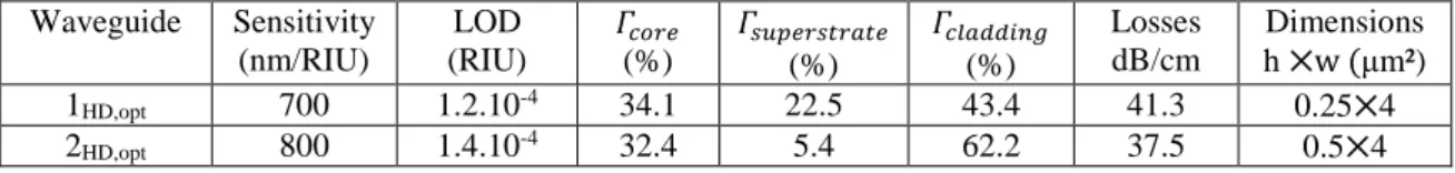
Table IV summarizes the best LOD and the associated sensitivity that can be obtained with optimal dimensions and optical losses (Fig.7.b) of single mode waveguides 1HDopt and 2HD opt for the two configurations
1HD and 2HD, studied. Table IV. Waveguide Sensitivity (nm/RIU) LOD (RIU) 𝛤𝑐𝑜𝑟𝑒 (%) 𝛤𝑠𝑢𝑝𝑒𝑟𝑠𝑡𝑟𝑎𝑡𝑒 (%) 𝛤𝑐𝑙𝑎𝑑𝑑𝑖𝑛𝑔 (%) Losses dB/cm Dimensions h ⨉w (μm²) 1HD,opt 700 1.2.10-4 34.1 22.5 43.4 41.3 0.25⨉4 2HD,opt 800 1.4.10-4 32.4 5.4 62.2 37.5 0.5⨉4
Optimal dimensions are detailed in table IV, for both configurations. Given that the waveguide height is small compared to single mode fiber core diameter, coupling between waveguide and fiber should be implemented with a fiber taper to decrease the coupling losses due to the mismatch of their mode field diameters. A gap between the access waveguide and the micro-ring resonator should be kept small in order to ease the evanescent coupling. Optical losses are reduced for configuration 2 compared to configuration 1 because of a higher distribution of the field intensity in the core and in the cladding ( 𝛤𝑐𝑜𝑟𝑒+ 𝛤𝑐𝑙𝑎𝑑𝑑𝑖𝑛𝑔).
The corresponding values are plotted in the pink area of the Fig.12 which represents sensitivity as a function of the LOD for different MR sensors.
Figure.12. Sensitivity as a function of LOD for different homogeneous MR sensors.
Fig.12 represents sensitivity as a function of the LOD for different MR sensors. As for surface sensing, different configurations of MR sensors have been fabricated. The first configuration developed by Iqbal et al., Kim et al., Liu et al. Guider et al. and Devos et al. are based on bulk material ridge waveguides (grey area)[11][13][43][9][44]. Then Carlborg et al., Claes et al., Barrios et al., Robinson et al. developed bulk material slot MR sensor (red area) to increase the interaction between the field and the solution [41][44][2][45]. Porous MR sensor have been developed recently in polymer by Mancuso et.al. [46], and in PSi by Rodriguez et al. and Girault
et al.[18][19] and have been optimized in this work by 1HD and 2HD MR sensors (pink area). These last devices principally improve the sensitivity.
By studying and then optimizing the waveguides of MR sensors, the characteristics of porous MR sensors have been enhanced. It can be noted that the MRs studied have a better sensitivity than the state of art because of the infiltration of analytes into the guiding layer adding to the evanescent detection. On the other hand, the LOD
15
is higher than those obtained by the best sensors of the state of the art because of the high losses induced by porous silicon and water absorption due to its infiltration into the guiding layer.
5. Conclusion
In this paper, MR based PSi waveguides for sensing detection have been studied to calculate the LOD and the sensitivity for surface and volume detection. The calculation of losses as a function of waveguide dimensions and refractive index difference have been estimated for both sensing techniques to predict the parameters of transducers. The influence of waveguide dimensions and porosity on sensitivity and LOD for both surface and homogeneous sensing have been developed by taking into account the different contributions of the waveguide optical losses. These calculations now give new guidelines for PSi waveguide design in case of sensing applications.
For surface sensing, a limit of detection of 0.5 pg.mm-2 and a sensitivity of 0.04 nm/(pg.mm-2) have been
calculated. These values are better than those obtained in the state of the art. A limit of detection of 1.2.10-4 RIU
and a sensitivity as high as 800 nm/RIU have been estimated for homogeneous detection. The volume homogeneous sensitivity calculated is better than the state of the art and the values of LOD are comparable to those obtained in the state of the art from bulk material based MR sensors.
In both cases, a lower refractive index difference leads to a lower LOD thanks to the reduction of surface scattering losses for higher waveguides dimensions. The possibility to detect analytes both in surface and homogeneous detection with the same waveguide material and dimensions could lead to interesting multiplexed sensing possibilities on a single chip. Moreover, such single MR could be integrated into a Vernier effect sensor to increase further both the sensitivity and the LOD [47].
Acknowledgment: This work is funded by Lannion Trégor Communauté, Région Bretagne and the
French government.
References
[1] A. Gutierrez-Arroyo, E. Baudet, L. Bodiou, J. Lemaitre, I. Hardy, F. Faijan, B. Bureau, V. Nazabal and J. Charrier, Optical characterization at 7.7 µm of an integrated platform based on chalcogenide waveguides for sensing applications in the mid-infrared, Optics Express 24(20) (2016) 23109-23117 https://doi.org/10.1364/OE.24.023109.
[2] C. A. Barrios, K. B. Gylfason, B. Sanchez, A. Griol, H. Sohlström, M. Holgado and R. Casquel, Slot-waveguide biochemical sensor, Optics Letters 32(21) (2007) 3080-3082https://doi.org/10.1364/OL.32.003080.
[3] C. A. Barrios, M. J. Banuls, V. Gonzales-Pedro, K. B. Gylfason, B. Sanchez, A. Griol, A. Maquieira, H. Sohlström, M. Holgado and R. Casquel, Label-free optical biosensing with slot-waveguides, Optics Letters 33(7) (2008) 708-710https://doi.org/10.1364/OL.33.000708.
[4] P. Kozma, F. Kehl, E. Ehrentreich-Förster, C. Stamm and F. Bier, Integrated planar optical waveguide interferometer biosensors: A comparative review, Biosensors and Bioelectronics 58 (2014) 287-307 https://doi.org/10.1016/j.bios.2014.02.049.
[5] Q. Liu, X. Tu, K. Kim, J. Sheng Kee, Y. Shin, K. Han, Y. Yoon, G. Lo and M. Park, Highly sensitive Mach-Zehnder interferometer biosensor based on silicon nitride slot waveguide, Sensors and actuators B 188 (2013) 681-688 https://doi.org/10.1016/j.snb.2013.07.053.
[6] S. Chakravarty, X. Chen, N. Tang, W. Lai, H. Yan and R. T. Chen, Review of design principles of 2D photonic crystal microcavity biosensors in silicon and their applications, Frontiers of Optoelectronics 9(2) (2016) 206-224 https://doi.org/10.1007/s12200-016-0631-2.
[7] A. Sana, K. Honzawa, Y. Amemiya and S. Yokoyama, Silicon photonic crystal resonators for label free biosensor, Japanese Journal of Applied Physics 55(4S) (2016) 04EM11.
16
[8] C. Ciminelli, F. Dell’olio, D. Conteduca, C. M. Campanella and M. N. Armenise, High performance SOI microring resonator for biochemical sensing, Optics & Laser Technology 59 (2014) 60-67 https://doi.org/10.1016/j.optlastec.2013.12.011.
[9] R. Guider, D. Gandolfi, T. Chalyan, L. Pasquardini, A. Samusenko, C. Pederzolli, G. Pucker and L. Pavesi, Sensitivity and Limit of Detection of biosensors based on ring resonators, Sensing and Bio-Sensing Research 6 (2015) 99-102https://doi.org/10.1016/j.sbsr.2015.08.002.
[10] K. D. Vos, J. Girones, S. Popelka, E. Schacht, R. Baets and P.Bienstman, SOI optical microring resonator with poly(ethylene glycol) polymer brush for labelfree biosensor applications, Biosensors and Bioelectronics 24(8) (2009) 2528-2533 https://doi.org/10.1016/j.bios.2009.01.009.
[11] M. Iqbal, M. A. Gleeson, B. Spaugh, F. Tybor, W. G. Gunn, M. Hochberg, T. Baehr-Jones, R.C. Bailey and L. C. Gunn, Label-free biosensor arrays based on silicon ring resonators and high-speed optical scanning instrumentation, IEEE Journal of Selected Topics in Quantum Electronics 16(3) (2010) 654-661 https://doi.org/10.1109/JSTQE.2009.2032510 .
[12] K. De Vos, I. Bartolozzi, E. Schacht, P.Bienstman and R. Baets, Silicon-on-Insulator microring resonator for sensitive and label-free biosensing, Optics Express 15(12) (2007) 7610-7615 https://doi.org/10.1364/OE.15.007610
[13] G. D. Kim, G. S. Son, H. S. Lee, K. D. Kim and S. S. Lee, Integrated photonic glucose biosensor using a vertically coupled microring resonator in polymers, Optics Communications, 281(18) (2008) 4644-4647 https://doi.org/10.1016/j.optcom.2008.06.006 .
[14] G.Rong and S.M.Weiss, Biomolecule size-dependent sensitivity of porous silicon sensors, Phys. Status Solidi A 206(6) (2009) 1365-1368 http://dx.doi.org/10.1002/pssa.200881097.
[15] J.Charrier, C.Lupi, L.Haji and C.Boisrobert, Optical study of porous silicon buried waveguides fabricated from p-type silicon, Materials Science in Semiconductor Processing 3(5-6) (2000) 357-361 https://doi.org/10.1016/S1369-8001(00)00056-1.
[16] E. Secret, K. Smith, V. Dubljevic, E. Moore, P.Macardle, B. Delalat, M. Rogers, T. G. Johns, J-O. Durand, F. Cunin and N. H. Voelcker, Antibody-functionalized porous silicon nanoparticles for vectorization of hydrophobic drugs, Advanced Healthcare Materials 2(5) (2013) 718-727 https://doi.org/10.1002/adhm.201200335.
[17] T. Hutter, N. Bamiedakis and S.R. Elliott, Theoretical study of porous silicon waveguides and their applicability for vapour sensing, Proceedings of COMSOL Conference, (2010)
[18] G A.Rodriguez, S. Hu, M. Weiss, Porous silicon ring resonator for compact, high sensitivity biosensing applications, OSA 23(6) (2015) 7111-7119https://doi.org/10.1364/OE.23.007111.
[19] P. Girault, P. Azuelos, N. Lorrain, L. Poffo, J. Lemaitre, P. Pirasteh, I. Hardy, M. Thual, M. Guendouz and J. Charrier, Porous silicon micro-resonator implemented by standard photolithography process for sensing application, Optical Materials 72 (2017) 569-601 https://doi.org/10.1016/j.optmat.2017.07.005.
[20] P. Girault, N. Lorrain, J. Lemaitre, L. Poffo, M. Guendouz, I. Hardy, M. Gadonna, A. Gutierrez,
L. Bodiou, J.Charrier, Racetrack micro-resonators based on ridge waveguides made of porous silica, Optical Materials 50(B) (2015) 167-174 https://doi.org/10.1016/j.optmat.2015.10.017.
[21] M. Hammer, K. R. Hiremath, R. Stoffer, Analytical approaches to the description of optical microresonator devices, Microresonators as Building Blocks for VLSI Photonics (2004) 48-71 http://dx.doi.org/10.1063/1.1764013.
[22] S. Dhanekar and S. Jain, Porous silicon biosensor: Current status, Biosensors and Bioelectronics 41 (2013) 54-64 https://doi.org/10.1016/j.bios.2012.09.045.
[23] J. Charrier and M. Dribek, Theoretical study of the factor of merit of porous silicon based optical biosensors, Journal of Applied Physics 107(4) (2010) http://dx.doi.org/10.1063/1.3295906.
[24] M. Hiraoui, M. Guendouz, N. Lorrain, A. Moadhen, L. Haji and M. Oueslati, Spectroscopy studies of functionalized oxidised porous silicon surface for biosensing applications, Materials Chemistry and Physics 128(1-2) (2011) 151-156 https://doi.org/10.1016/j.matchemphys.2011.02.052.
[25] E.V. Astrova, V.B. Voronkov, A.D. Remenyuk, V.B. Shuman and V.A. Tolmachev, Variation of the parameters and composition of thin films of porous silicon as a result of oxidation: ellipsometric studies, Semiconductors 33(10) (1999) 1149-1155 https://doi.org/10.1134/1.1187885.
[26] I.M. White and X. Fan, On the Performance quantification of resonant refractive index sensors, Optics Express 16(2) (2008) 1020-1028 https://doi.org/10.1364/OE.16.001020.
[27] D. V. Strekalov, R. J. Thompson, L. M. Baumgartel, I. S. Grudinin and N. Yu, Temperature measurement and stabilization in a birefringent whispering gallery mode resonator, Optics Exrpress 19(15) (2011) 14495-14501 https://doi.org/10.1364/OE.19.014495.
17
[28] V.D. Bruggeman, Berechnung verschiedener physikalischer konstanten von heterogenen substanzen. i. dielektrizitätskonstanten und leitfähigkeiten der mischkörper aus isotropen substanzen, Ann Phys 416(7) (1935) 636–664 http://dx.doi.org/10.1002/andp.19354160705.
[29] A. B. Fallahkhair, K. S. Li and T. E. Murphy, Vector Finite Difference Modesolver for Anisotropic Dielectric Waveguides, J. Lightwave Technol. 26(11) (2008) 1423-1431
http://dx.doi.org/10.1109/JLT.2008.923643.
[30] P. Pirasteh, J. Charrier, Y. Dumeige, S. Haesert and P. Joubert, Optical loss study of porous silicon and oxidized porous silicon planar waveguides, Journal of applied Physics 101(8) (2007) 083110 http://dx.doi.org/10.1063/1.2718886.
[31] F.P. Payne, J.P.R. Lacey, A theoretical analysis of scattering loss from planar optical waveguides, Optical and quantum Electronics 26(10) (1994) 977-986 https://doi.org/10.1007/BF00708339.
[32] F. Grillot, L. Vivien, E. Cassan and S. Laval, Influence of waveguide geometry on scattering loss effects on submicron strip silicon-on –insulator waveguides, IET Optoelectronics 2(1) (2008) 1-5 https://doi.org/10.1049/iet-opt:20070001.
[33] J. Charrier, Y. Dumeige, P. Pirasteh and M. Gadonna, Effect of interface roughness and polarization on the optical losses of porous silicon-based waveguides, IET Micro&Nano Letters 7(3) (2012) 275-278 https://doi.org/10.1049/mnl.2012.0027.
[34] V. Chamard, P. Bastie, D. Le Bolloch, E. Elkaïm, C. Ferrero, J.-P. Lauriat, F. Rieutord and D. Thiaudière, Evidence of pore correlation in porous silicon: An x-ray grazing-incidence study, Physical Review B 64(24) (2001) 245416 http://dx.doi.org/10.1103/PhysRevB.64.245416.
[35] A. Kirchner, K. Busch and C.M. Soukoulis, transport properties of random arrays of dielectric cylinders, Physical review B 57(1) (1998) 277-288 http://dx.doi.org/10.1103/PhysRevB.57.277.
[36] J.L. Lawrie , Y. Jiao and S.M. Weiss, Size-Dependent infiltration and optical detection of nucleic acids in nanoscale pores, IEEE transactions of nanotechnology 9(5) (2010) 596-602
https://doi.org/10.1109/TNANO.2010.2055580.
[37] J.A. Cursio and C.C. Petty, The near infrared absorption spectrum of liquid water, Journal of the optical society of America 41(5) (1951) 302-304 https://doi.org/10.1364/JOSA.41.000302.
[38] M.H. Chan, S.K. So and K.W. Cheah, Optical absorption of free standing porous silicon films, J. Appl. Phys. 79(6) (1996) 3273-3275 http://dx.doi.org/10.1063/1.361216.
[39] M.S. Luchansky, A.L. Washburn, T.A. Martin, M. Iqbal, L.C. Gunn and R.C. Bailey, Characterization of the evanescent field profile and bound mass sensitivity of a label-free silicon photonic microring resonator biosensing platform, Biosensors and bioelectronics 26(4) (2010) 1283-1291 https://doi.org/10.1016/j.bios.2010.07.010. [40] D. X. Xu, A. Densmore, A. Delage, P. Waldron, R. McKinnon, S. Janz, J. Lapointe, G. Lopinski, T. Mischki, E. Post, P. Cheben and J. H. Schmid, Folded cavity SOI microring sensors for high sensitivity and real time measurement of biomolecular binding, Optics Express 16(19) (2008) 15137-15148 https://doi.org/10.1364/OE.16.015137.
[41] C. F. Carlborg, K. B. Gylfason, A. Kazmierczak, F. Dortu, M. J. Banuls Polo, A. Maquieira Catala, G. M. Kresbach, H. Sohlström, T. Moh, L. Vivien, J. Popplewell, G. Ronan, C. A. Barrios, G. Stemme and W. Van Der Wijingaart, A packaged optical slot-waveguide ring resonator sensor array for multiplex label-free assays in labs-on-chips, Lab on a Chip 10(3) (2010) 257-396 https://doi.org/10.1039/b914183a
[42] J. Liu, X. Zhou, Z. Qiao, J. Zhang, C. Zhang, T. Xiang, L. Shui, Y. Shi and L. Liu, Integrated optical chemical sensor based on an SOI ring resonator using Phase-Interrogation, IEEE Photonics Journal 6(5) (2014) 6802207 https://doi.org/10.1109/JPHOT.2014.2352973.
[43] K.D. Vos, I. Bartolozzi, E. Schacht, P. Bienstman and R. Baets, Silicon-on-Insulator microring resonator for sensitive and label-free biosensing, Optics Express 15(12) (2007) 7610-7615 https://doi.org/10.1364/OE.15.007610.
[44] T. Claes, J. G. Molera, K. De Vos, E. Schacht, R. Baets and P. Bienstman, Label-Free biosensing with a slot-waveguide-based ring resonator in silicon on insulator, IEEE Photonics Journal 1(3) (2009) 197-204 https://doi.org/10.1109/JPHOT.2009.2031596.
[45] J. T. Robinson, L. Chen and M. Lipson, On-chip gas detection in silicon optical microcavities, Optics Express 16(6) (2008) 4296-4301 https://doi.org/10.1364/OE.16.004296.
[46] M. Mancuso, J. M. Goddard and D. Erickson, Nanoporous polymer ring resonators for biosensing, Optics Express 20(1) (2012) 245-255 https://dx.doi.org/10.1364/OE.20.000245
[47] P. Azuelos, P. Girault, N. Lorrain, L. Poffo, I. Hardy, M. Guendouz and M. Thual, Theoretical investigation of Vernier effect based sensors with hybrid porous silicon-polymer optical waveguides Journal of Applied Physics 121(14) (2017) 144501 http://dx.doi.org/10.1063/1.4980010.