HAL Id: hal-00350358
https://hal.archives-ouvertes.fr/hal-00350358
Submitted on 28 May 2019HAL is a multi-disciplinary open access archive for the deposit and dissemination of sci-entific research documents, whether they are pub-lished or not. The documents may come from teaching and research institutions in France or abroad, or from public or private research centers.
L’archive ouverte pluridisciplinaire HAL, est destinée au dépôt et à la diffusion de documents scientifiques de niveau recherche, publiés ou non, émanant des établissements d’enseignement et de recherche français ou étrangers, des laboratoires publics ou privés.
Modelling of a Capacitance-to-Period Converter
Dedicated to Capacitive Sensors
Philippe Menini, Philippe Dondon, G. Blasquez, Patrick Pons
To cite this version:
Philippe Menini, Philippe Dondon, G. Blasquez, Patrick Pons. Modelling of a Capacitance-to-Period Converter Dedicated to Capacitive Sensors. EUROSENSORS XIII, Sep 1999, LA HAYE, Netherlands. pp.279. �hal-00350358�
Modelling of a Capacitance-to-Period Converter
Dedicated to Capacitive Sensors
Ph. Ménini1, Ph. Dondon2 , G. Blasquez1 and P. Pons1. 1
CNRS LAAS , 7 Avenue du Colonel Roche, 31 077 Toulouse cedex 4 France -2
IXLBordeaux1, 351 Cours de la Libération, 33405 Talence cedex France
-SUMMARY
This paper analyses a BiCMOS integrated circuit for interfacing capacitive sensors. A demonstrator has been implemented to evaluate its actual behaviour. This converter is based on the charge and the discharge of a capacitor with a constant current. A simple analytical model as first-order theory has been compared with PSPICE simulations and experimental data. Significant errors reveal the influence of leakage currents, stray capacitors and interference due to clock feedthrough and charge injection phenomena. Analytical and electrical models have been extended to include these parasitic parameters and simulate properly their thermal behaviour. Experimental data show close agreement between these models and practice.
Keywords : Capacitive pressure sensors, BiCMOS converter, PSPICE, Modelling.
INTRODUCTION
Since few years, research on microsystems and multi-sensor networks requires concomitant development of digital-output sensors to make them compatible with communication network. This work takes place in the study of a digital-output capacitive pressure sensor which consists of a capacitive silicon/Pyrex sensing cell and a BiCMOS integrated circuit. This transducer is based on a capacitance ratio to frequency ratio conversion in order to procure a high level of self-compensation for temperature drifts and non-linearity [1].
The demonstrator presented hereafter has permitted to elaborate simple analytical and electrical models of the analog part of the integrated circuit which includes two capacitance-to-period converters. This type of converter procures a linear response (period time) with respect to capacitance. Experimental results have permitted to validate these two models and will allow us to discuss on potentialities of this sensor.
DESCRIPTION AND MODELLING
This converter has been designed to generate a triangular waveform with time period proportional to the capacitance. It operates on the principle of charge and discharge of a capacitor with constant current Io, between
two threshold voltages VL and VH. This type of oscillator
can be electrically modelled by a charging current source (Io), a discharging one (2Io), a
Metal-Oxide-Semiconductor Transistor (MOST) switch and a Control Logic Circuit (CLC) that drives the on and the turn-off. The CLC consists of two threshold NPN-input comparators and a RS logic-gate.
Considering the switching delay Δt that includes CLC time response and intrinsic MOS switching time, the
theoretical time period T of the triangular waveform signal is given by the analytical relation :
T = τd + k × C (1)
where τd≈ 4 Δt and k = 2(VH-VL)/Io.
Even if the CLC has been designed with fastest components, the offset τd remains close to 350 ns. By
design, the peak-to-peak amplitude (VH - VL) of the
oscillations is equal to 1.2 V and the theoretical current value Io is 20.2 μA.
An electrical model of this analogue block which includes two oscillators has been implemented in PSPICE level 2 taking original component feature into account.
EXPERIMENTAL RESULTS
An universal period-meter and different ceramic capacitors have permitted to evaluate the converter response with a good resolution (0.01 % of the measured value).
Experimental measurements of period-data with capacitances varying from 10 pF to 100 pF are reported in Fig. 1. They are compared with simple analytical model and PSPICE simulation.
0 20 40 60 80 100 0 2 4 6 8 10 12 14 Exp. Pspice Analyt. T ( µ s) Capacitance (pF)
Fig. 1 : Converter response.
It can be seen that the experimental offset value is greater than that expected with only the switching delay τd. That
reveals the existence of stray capacitors Cs which have
been evaluated in the order of 3.3 pF. Slope differences are explained by an error on current value due to resistance (Rs) disparities. Effectively, Io has been
experimentally measured close to 20.4 μA.
Detailed analysis of output signals reveal, on one hand, a slight difference between charging current value (Ic) and
the discharging current one (Id). Moreover, these currents
are time dependent during their "own" half-period. That is explained by the existence of a leakage current If, but also,
it coexists problem of current gain error in current mirrors and the non-negligible output conductance in small-size MOS transistors. Essentially due to comparators’ input offset current, If has been estimated of the order of 450
nA. On the other hand, it has been observed a voltage pulse on the triangular waveform at the switching time. Even if integrated switches are used, clock feedthrough and charge injection during the turn-on and the turn off of the switch remain non-negligible when measured capacitance is of the order of 10 pF. This problem will be developed in the full paper.
Thermal behaviour
Figure 2 shows experimental and theoretical relative thermal variations of period with a constant ceramic capacitor. The theoretical one is obtained by introducing only the current source thermal behaviour as indicated on the IC data sheet.
-20 0 20 4 0 60 8 0 1 00 1.00 1.01 1.02 1.03 1.04 1.05 θ (°C ) T / T(25°C ) The or. Exp .
Fig. 2 : Comparison between theoretical and experimental data on relative period variations with temperature.
These results indicate that Cs and If make the converter’s
thermal drifts much more important. More detailed measurements have permitted to evaluate their thermal behaviour and then introduce them in analytical and PSPICE models.
EXTENDED MODELS
The more realistic analytical expression of the period tacking If and Cs into account is :
(
s)
d K C C
T = τ + × + (2)
where K = k/[1-(If/Io)2]
Anyway, converter sensitivity is quasi-unchanged until Zin
(equivalent comparators’ input impedance) is much more greater than Zc (equivalent impedance of measured
capacitor).
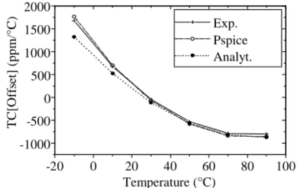
Validation of this model has been obtained by comparing period response but also, offset temperature coefficient with measurements (Fig. 3). As opposed to PSPICE simulation, it appears that the simple analytical model is slightly different to experimental data. Effectively, temperature behaviour of all transistors are not considered in eqn. (2). -20 0 20 40 60 80 100 -1000 -500 0 500 1000 1500 2000 Exp. Pspice Analyt. TC[Offs et] (ppm/° C) Temperature (°C)
Fig. 3 : Offset temperature coefficient of frequency output.
From relation (2), assuming that τd is invariant and the
thermal drift of threshold voltages are negligible, the more realistic thermal behaviour of the converter can be defined by :
(
)
⎥ ⎦ ⎤ ∂ ⎟⎟⎠ ⎞ ⎜⎜⎝ ⎛ χ − χ + ∂ ⎟⎟⎠ ⎞ ⎜⎜⎝ ⎛ χ − χ + − ⎢ ⎣ ⎡ ∂ ⎟⎟⎠ ⎞ ⎜⎜⎝ ⎛ β + β + ∂ ⎟⎟⎠ ⎞ ⎜⎜⎝ ⎛ β + α − = ∂ f f o o s s I I 1 2 I I 1 1 C C 1 C C 1 1 1 T T (3) with α = τd/T, β = Cs/C and χ = (If/Io)2.If α, β, χ << 1, period thermal drifts are determined by those of the current source and the capacitor C. As χ is already very low, these conditions are realised when C >> Cs (C ≈ 100 pF).
CONCLUSION
This paper has introduced a BiCMOS integrated circuit for interfacing capacitive sensors. Based on the charge and the discharge of capacitor with constant current, the analog part of the converter has been described with a simple analytical model and an electrical one implemented in Pspice software. First-order analysis has led to inaccurate estimations of converter behaviour. The differences have been shown to be caused by the existence of leakage currents, stray capacitors and charge injection during turn-on and turn-off of MOS switches. The easiest improvement to minimise significantly the leakage current consists in replacing the NPN-input comparators by NMOS-input comparators. Anyway, as the two extended models present close agreement with experimental data, they can be used to simulate sensor behaviour and then to find some solutions to optimise it.
REFERENCES
[1] G. Blasquez, P. Pons, Ph. Menini, X. Chauffleur, Ph. Dondon and C. Zardini, "Efficiency of a BiCMOS
ratiometric circuit to self-compensate for non-linearities and thermal drifts in capacitive pressure sensors", EurosensorX,