HAL Id: tel-01665811
https://pastel.archives-ouvertes.fr/tel-01665811v2
Submitted on 17 Jan 2018
HAL is a multi-disciplinary open access
archive for the deposit and dissemination of
sci-entific research documents, whether they are
pub-lished or not. The documents may come from
teaching and research institutions in France or
abroad, or from public or private research centers.
L’archive ouverte pluridisciplinaire HAL, est
destinée au dépôt et à la diffusion de documents
scientifiques de niveau recherche, publiés ou non,
émanant des établissements d’enseignement et de
recherche français ou étrangers, des laboratoires
publics ou privés.
Carbone : Mécanismes et Applications pour le Stockage
de Données
Loïc Loisel
To cite this version:
Loïc Loisel. Claquage Electrique et Optique d’Allotropes du Carbone : Mécanismes et Applications
pour le Stockage de Données. Physique [physics]. Université Paris Saclay (COmUE); Nanyang
Tech-nological University, 2016. Français. �NNT : 2016SACLX021�. �tel-01665811v2�
NNT : 2016SACLX021
THESE DE DOCTORAT DE
LA NANYANG TECHNOLOGICAL UNIVERSITY
ET DE L'UNIVERSITE PARIS-SACLAY
préparée à
LA NANYANG TECHNOLOGICAL UNIVERSITY
et à
L'ECOLE POLYTECHNIQUE
ÉCOLE DOCTORALE
Interfaces - Approches interdisciplinaires: fondements, applications et innovations
Spécialité de doctorat : Physique
par
Loïc LOISEL
Optical and Electrical Breakdown of Carbon Allotropes:
Mechanisms and Applications for Data Storage
Thèse présentée et soutenue à l'Ecole Polytechnique, le 13 avril 2016 Composition du jury :
M. Qing ZHANG Président Nanyang Technological University M. Daniel CHUA Examinateur National University of Singapore M. Henri-Jean DROUHIN Examinateur Ecole Polytechnique
Mots clés : stockage de données, mémoires, recuit laser, carbone, graphène, commutateur électro-mécanique
Résumé : Aujourd'hui, les applications de stockage de donnés utilisent principalement deux types de matériaux: les chalcogénures pour le stockage optique (e.g. Blu-Ray) et le silicium pour le stockage électronique (e.g. mémoires Flash). Malgré le fait qu'ils se soient avérés les plus e caces pour des applications répandues, ces matériaux ont des limitations. Récemment, avec la montée en puissance du graphène, les allotropes du carbone ont été étudiés à la fois pour leurs propriétés intrinsèques et pour des applications; ils ont des propriétés électroniques, thermiques et mécaniques très intéressantes qui peuvent rendre ces matériaux plus e caces que les chalcogénures ou le silicium pour certaines applications. Dans cette thèse, nous étudions la faisabilité et le potentiel du carbone comme matériau pour le stockage de données.
Nous nous concentrons d'abord sur le développement de stockage optique. Nous découvrons que les lasers continus et pulsés peuvent être utilisés pour induire des changements de phase réversibles dans des couches minces de carbone, con rmant la possibilité d'utiliser le carbone comme un matériau pour le stockage optique. De plus, nous découvrons plusieurs nouveaux phénomènes, que nous expliquons en utilisant des techniques de caractérisation avancées et la modélisation par ordinateur de la propagation thermique dans le carbone.
Ensuite, nous nous concentrons sur le stockage de données électronique en développant des mémoires à base de graphène qui peuvent être dans deux états de résistance bien séparés pour un grand nombre de cycles. Pour évaluer le potentiel de cette technologie, on caractérise le mécanisme de changement de résistance et on développe un modèle électromécanique qui permet de prédire les meilleures performances atteignables : ces mémoires ont le potentiel de commuter bien plus rapidement que les mémoires Flash tout en étant non-volatiles. Title : Optical and Electrical Breakdown of Carbon Allotropes: Mechanisms and Applications for Data Storage
Keywords : data storage, memory, laser annealing, graphene, electro-mechanical switch
Abstract : Today, data storage applications rely mainly on two types of materials: chalcogenides for optical storage (e.g. Blu-Ray) and silicon for electronic storage (e.g. Flash memory). While these materials have proven to be the most e cient for widespread applications, both have limitations. Recently, with the rise of graphene, carbon allotropes have been studied both for their intrinsic properties and for applications; graphene and other carbon allotropes have very interesting electronic, thermal and mechanical properties that can make these materials more e cient than either chalcogenides or silicon for certain applications. In this thesis, we study the feasibility and potential of the usage of carbon as a data storage material.
Firstly, we focus on developing optical data storage. It is found that both continuous-wave and pulsed lasers can be used to induce reversible phase changes in carbon thin lms, thus opening the way toward carbon-based data storage. Along the way, several phenomena are discovered, shown and explained by using advanced characterization techniques and thermal modelling.
Secondly, we focus on electronic data storage by developing graphene-based memories that are found to switch reliably between two well-separated resistance states for a large number of cycles. To assess the potential of this new technology, we characterize the switching mechanism and develop an electro-mechanical model enabling to predict the best performances attainable: these memories would potentially be much faster than Flash memories while playing the same role (non-volatile storage).
Université Paris-Saclay
Espace Technologique / Immeuble Discovery
Les technologies informatiques ont un impact important sur les sociétés actuelles et sur leur évolution. Elles ont des besoins importants en termes de stockage de données. Il existe plusieurs façons de stocker des données qui sont plus ou moins adaptées à des besoins spécifiques. En particulier, on peut distinguer deux familles de technologies: le stockage de données électronique et le stockage optique. Un exemple de stockage de données optique est la technologie Blu-Ray, pour laquelle un laser est utilisé pour écrire et/ou lire des données sur un disque. Un exemple de stockage de données électronique est la technologie Flash, pour laquelle une tension électrique est appliquée aux deux bornes d’un transistor, et la quantité de courant électrique qui est lue dépend de son état: soit "ON" soit "OFF" (lecture). Pour modifier la quantité de courant qui passe (écriture), on applique une tension à une troisième partie du transistor appelée "la grille".
Les matériaux les plus utilisés pour ces deux types de technologie sont le silicium (stock-age électronique) et les chalcogénures (stock(stock-age optique). Jusqu’à aujourd’hui, le sili-cium a été le meilleur compromis pour le stockage électronique pour plusieurs raisons: grande disponibilité, oxydation aisée pour créer l’oxyde de grille du transistor, progrès rapides liés au grand rythme de miniaturisation du transistor (loi de Moore), etc... Les chalcogénures, quant à eux, sont utilisées pour des applications de stockage optique grâce aux basses températures nécessaires pour changer leur état de cristallinité (tem-pérature de cristallisation ou de fusion). Des tem(tem-pératures d’écriture plus basses mènent à des besoins énergétiques plus faibles, et donc à une baisse du coût de la technologie. Néanmoins, il existe des domaines dans lesquels ces matériaux n’excellent pas, et sur
RESUME 5 lesquels des efforts de recherche se concentrent aujourd’hui.
Jusqu’à présent, pour le stockage de données électronique, il a été nécessaire d’utiliser plusieurs technologies complémentaires afin d’obtenir les meilleurs performances car il n’y a pas de composant électronique qui soit à la fois peu cher, rapide, non volatile (qui garde l’information même quand le système est éteint), et qui permette de stocker de très grande densités d’information sur une petite surface. Ainsi l’architecture des ordi-nateurs comprend plusieurs types de mémoires à plusieurs endroits et qui ont plusieurs rôles complémentaires. Aujourd’hui, il n’y a donc pas de moyen de se passer de cette complexité. Mais de nombreux instituts de recherche et entreprises sont à la recherche d’une technologie qui soit à la fois peu chère, rapide, non volatile et qui permette de stocker de larges quantités de données. La découverte d’une telle technologie perme-ttrait de grandement améliorer les architectures informatiques, en minimisant grande-ment leur complexité.
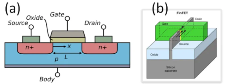
Un autre problème lié à l’utilisation du silicium est qu’à force de miniaturiser les tran-sistors pour améliorer leurs performances, leurs dimensions se rapprochent de la lim-ite atomique, ce qui mène à plusieurs problèmes liés à des phénomènes quantiques (courants de fuite, variabilité des implantations de dopants...) et, de toute manière, la limite de l’atome est une limite qui ne pourra pas être dépassée avec les approches actuelles. Bien que les technologies à base de silicium soient mâtures, des défis im-portants existent toujours aujourd’hui, qu’il semble difficile de résoudre en n’utilisant qu’elles.
Pour ce qui est du stockage optique, la principale qualité des chalcogénures peut aussi s’avérer être un défaut: comme leurs températures de changements de structure (cristalli-sation, fusion) sont basses, ils peuvent s’avérer instables dans des conditions extrêmes, telles que l’espace (exposition à des rayonnements énergétiques, températures et vari-ations de températures extrêmes). Trouver des matériaux plus stables à hautes tem-pératures peut donc s’avérer intéressant pour des applications dans l’aérospatiale, par exemple.
Dans cette thèse, on se propose d’explorer le potentiel du carbone comme matériau de base pour le stockage de données optique et électronique.
Pour les applications optiques, la température de fusion du carbone est bien plus élevée que celle des chalcogénures ; ainsi, sa structure devrait être plus résistante à des con-ditions extrêmes. Pour ce qui est des applications électroniques, certains allotropes du carbone ont été synthétisés pour la première fois assez récemment (par exemple le graphène, en 2004), et il a été montré que certaines de leurs propriétés électroniques sont supérieures à celles du silicium (par exemple, la mobilité des porteurs de charge). Pour le stockage optique, l’état de l’art sur les interactions laser-carbone montre qu’il n’y a pour l’instant pas de démonstration de changement de phase réversible, ce qui est un défi à relever si on veut réaliser des mémoires optiques réversibles. On réalise également que les mécanismes de changement de phase sont assez peu compris, que ce soit dans le cas de recuits laser continus (application d’un flux lumineux continu) ou dans le cas de recuits laser pulsés (applications de "pulses" de lumière très rapides).
En premier lieu (Chapter 3), on étudie les recuits laser continus de couches minces de graphite nanocristallin. Bien qu’un changement de phase réalisé par un laser continu soit, par définition, plus long qu’un changement de phase réalisé par un laser pulsé, on estime que les phénomènes observés seront plus aisés à comprendre, et on pourra donc ensuite se baser sur cette compréhension pour travailler avec des lasers pulsés (Chapter 4). On utilise des couches minces de graphite nanocristallin car la structure de ce matériau peut être classée entre celle du carbone amorphe et du graphite: des cristaux de graphite sont entourés de carbone amorphe. C’est une structure cristalline idéale pour étudier des changements de phase car elle permet de les étudier dans les deux directions: changements de phase vers une structure plus cristalline ou vers une structure plus amorphe.
On découvre que l’application d’une puissance laser suffisante mène à plusieurs phénomènes: pour les plus hautes énergies, une perte de matière ainsi qu’une amorphisation de la structure, tous deux observés par microscopie électronique à transmission (MET). Pour des énergies plus faible, bien qu’il n’y ait pas de changements cristallin directement ob-servables par MET à haute résolution, localement la conductivité électrique est grande-ment auggrande-mentée (microscopie à force atomique en mode conduction) ; ce changegrande-ment est couplé à une légère augmentation de la hauteur moyenne de la couche. Ces deux faits
RESUME 7 suggèrent qu’un phénomène de graphitisation a lieu pendant le recuit, car le graphite est plus conducteur électriquement que le carbone amorphe, et il est également moins dense (il prend plus de place). Nous contrôlons également l’évolution du signal Raman réémis par le matériau situ (durant le recuit), ce qui nous permet d’obtenir des in-formations sur la structure cristalline pendant le recuit. L’évolution des pics I(D)/I(G) et de la largeur du pic G indiquent un phénomène d’amorphisation, ce qui va dans le sens de ce qu’on observe au MET. En revanche, l’évolution de la position du pic G semble indiquer un phénomène de graphitisation. Or, le pic G est sensible à d’autres paramètres que la structure cristalline, tels que la température ou encore la concentra-tion de dopants. De plus, le carbone peut être dopé positivement quand il interagit avec de l’oxygène. On décide donc d’étudier la présence d’éléments chimiques dans les couches recuites grâce à un spectromètre dispersif en énergie, et on observe en effet une plus forte présence d’oxygène aux endroits recuits, jusqu’à des profondeurs proches de la profondeur du phénomène d’amorphisation observé au MET. Ainsi, ces résultats suggèrent que l’amorphisation ainsi que l’évolution de la position du pic G pendant le recuit sont tous deux dus à des phénomènes d’oxydation. La perte de matière est cer-tainement également provoquée par des réactions avec l’oxygène ambiant, car la tem-pérature d’oxydation (par émission de molécules gazeuses de CO et de CO2) du carbone
est bien inférieure à sa température de fusion (environ 4450K). De plus, on n’observe aucun dommage sur la couche de titane présente sous le carbone, ce qui suggère que des températures supérieures à la température de fusion du titane (environ 1941K) ne sont pas atteintes durant le recuit.
Dans cette étude, on a donc montré qu’il est possible d’obtenir des changements de phase dans les deux directions (amorphisation et graphitisation) via l’application d’un faisceau laser continu. L’amorphisation et la perte de matière sont liés à des réactions avec l’oxygène environnant, et tous les changements se font à l’état solide. On a égale-ment montré que cette technique peut être utilisée pour écrire des motifs conducteurs. Mais les échelles de temps nécessaires étant longues, on cherche dans le chapitre suiv-ant (Chapter 4) à utiliser un laser pulsé pour induire des changements dans des couches minces de carbone de même nature.
Au début de notre étude sur les recuits laser pulsés, l’état de l’art suggérait qu’il était très difficile, voire impossible, d’amorphiser le carbone. Notre premier but était donc d’amorphiser le graphite nanocristallin. Pour cela, on décide d’utiliser des pulses lu-mineux plus énergétiques que ceux généralement utilisés dans la littérature. On réalise une étude systématique de recuits laser en augmentant peu à peu l’énergie jusqu’à un maximum de 15.4 J.cm2. Pour des énergies faibles, on observe un phénomène de
graphi-tisation qui est déjà décrit dans la littérature. Néanmoins, en augmentant l’énergie, on atteint un plateau de graphitisation, et l’application de pulses plus énergétiques mène graduellement à un matériau plus amorphe. Ces résultats sont confirmés par MET à haute résolution et par spectroscopie Raman. Le premier objectif de l’étude étant réalisé, on teste l’endurance du processus réversible (car on peut graphitiser et amorphiser). On trouve que l’endurance est très limitée, à deux ou trois cycles (un cycle = graphitisation puis amorphisation), et on décide donc d’étudier l’état de la surface après les recuits, afin d’étudier les dégradations causées par les recuits énergétiques. Grâce à un microscope électronique à balayage, on observe différentes formes de dégradations apparaissant à différentes énergies: la croissance de grains (signe de fusion), cracks, vagues, sphères, piliers pleins ou creux, et enfin la présence de structures labyrinthiques qui suggèrent qu’aux hautes énergies nécessaires pour l’amorphisation, des phénomènes de fusion plosive apparaissent. Une grande partie de ces dégradations sont irréversibles et ex-pliquent donc la faible endurance que l’on a observé. Elles montrent également que même aux plus faibles densités d’énergie utilisées dans cette étude, au moins une par-tie du carbone est fondue. Ce fait contraste fortement avec les résultats que nous avons obtenus avec un laser continu (Chapter 3). Nous effectuons des simulations par éléments finis, qui nous permettent d’estimer les températures atteintes et les durées nécessaires pour les atteindre: on trouve que la température en surface monte très rapidement (en moins de 10 nanosecondes) à des températures suffisantes pour fusionner le carbone, tandis que les durées nécessaires à l’oxydation du carbone qui sont rapportées dans la littérature sont bien plus longues. L’oxydation ne joue donc pas un rôle prépondérant ici, contrairement au cas du recuit laser continu (Chapter 3). Les simulations nous per-mettent également de comparer les vitesses de refroidissement après avoir atteint la température maximale, et les gradients thermiques dans les couches lors du
refroidisse-RESUME 9 ment. Cela nous permet de savoir si l’amorphisation se fait par refroidissement rapide (comme pour le verre) ou par solidification homogène (comme, dans certains cas, pour le silicium). On trouve que la solidification homogène est le phénomène qui mène à l’amorphisation ici: la solidification se fait de manière homogène quand le carbone reste à l’état liquide assez longtemps pendant le refroidissement pour que les gradients de température soient faibles quand la température de solidification est atteinte. Dans ce cas, il n’y a pas (ou peu) de noyaux de cristallisation solides restants dans la matière pour agir comme catalyseurs de la cristallisation du matériau liquide. La graphitisa-tion, quant à elle, est obtenue à des énergies plus faibles pour lesquels des gradients de température existent lors de la solidification: il y a donc une solidification hétérogène, et le carbone liquide devient solide en contact avec du carbone solide qui agit comme catalyseur de la cristallisation.
On a donc démontré que le carbone a un potentiel comme matériau de base pour stocker des données. Pour améliorer l’endurance, il faudrait trouver un moyen de graphitiser et d’amorphiser avec moins de dégradations. Une piste est l’utilisation de pulses fem-toseconde au lieu de pulses nanoseconde: certains articles de la littérature mentionnent qu’il est possible d’amorphiser de la matière de façon "non thermique" en utilisant des pulses femtoseconde. On a mis en place un banc optique de recuit laser femtoseconde, et pour l’instant, nous avons obtenu des résultats préliminaires qui sont décrits dans ce manuscrit.
Le deuxième objectif de cette thèse est d’étudier la possibilité de fabriquer des mémoires électroniques à base de carbone, qui seraient à la fois rapides, non-volatiles, et qui pour-raient être fabriquées avec de fortes densités de surface.
En particulier, ici nous avons décidé de nous concentrer sur un type de dispositif à base de graphène, un allotrope du carbone consistant en une couche d’atomes de carbone arrangée en nids d’abeilles. Il y a un débat dans la littérature sur un certain type de dis-positif en particulier ; ces disdis-positifs sont faits de deux électrodes posées sur une bande de graphène, et auxquels on a appliqué une très forte tension qui a mené à leur claquage électrique. Il a été montré que le claquage est dû à l’apparition d’un crack qui se propage perpendiculairement au champ électrique, et qui coupe la bande de graphène en deux,
ce qui mène à une conductivité nulle (mis à part des effets tunnels pour lesquels les élec-trons traversent le vide). Ensuite, il a été démontré qu’il est possible de revenir à un état de résistance bien plus basse, et vice-versa. Ces états de résistance réversibles sont non volatils, et des vitesses de commutation de 100 ns ont été démontrées. Bien que ce ne soit pas aussi rapide que la commutation des mémoires vives statiques ou dynamiques, ces résultats préliminaires sont très encourageants. Néanmoins, la compréhension du mécanisme de commutation n’est pas complète: deux modèles s’opposent. Certains au-teurs proposent qu’à partir du claquage électrique, le graphène n’est plus le matériau actif, mais que le changement de résistance se fait dans le substrat d’oxyde de silicium (SiO2). La commutation se ferait donc par création/destruction de filaments de
sili-cium dans le SiO2ou réduction/oxydation du SiO2. D’autres auteurs proposent que le
graphène est bien le matériau actif: il ferme/ouvre le crack en se déplaçant de manière réversible. Bien qu’il y ait des indices favorisant fortement les deux hypothèses, certains chercheurs pensent que le premier modèle (SiO2) est plus solide, car le second modèle
propose peu d’explications pour les phénomènes décrits. En particulier, on ne sait pas quelles forces contrôlent l’ouverture/fermeture du crack, ni la non-volatilité.
Ici, on cherche à fabriquer des mémoires non-volatiles à base de graphène et à compren-dre leur mécanisme de commutation, en prenant en compte ce débat (Chapter 5). En premier lieu, on montre que l’on obtient des dispositifs qui commutent de manière non-volatile, pour 500 cycles dans le meilleur des cas, et avec des contrastes de résistance aussi élevés que 104 (pour 125 cycles). Ensuite, on observe le crack par microscopie à
force atomique: quand un dispositif conduit (état "ON"), on trouve qu’à certains en-droits du crack, des "ponts" de graphène sont présents, ce qui explique la plus grande conductivité. A l’état "OFF", nous ne trouvons pas de trace de ces ponts. Ainsi, il semble que dans notre cas, l’hypothèse de commutation par mouvements du graphène peut être privilégiée. De plus, les performances de nos dispositifs, surtout en termes de temps de commutation (aux alentours d’une seconde), sont similaires aux autres dispositifs dont la commutation est expliquée par le mouvement du graphène. Les deux mécanismes de commutation pourraient donc bien coexister dans différents dispositifs.
RESUME 11 veut pouvoir estimer le potentiel de cette technologie, et trouver des moyens pour l’améliorer. En appliquant des bilans d’énergie au système graphène + crack, on montre qu’un mod-èle purement électro-mécanique permet d’expliquer le déplacement dans les deux sens (fermeture du crack par les forces d’attraction de Coulomb lorsqu’on applique une ten-sion électrique, ouverture du crack par les forces élastiques du graphène en l’absence de tension électrique). En revanche, ce modèle ne permet pas d’expliquer la non-volatilité et les performances limitées en termes de vitesse de commutation et d’endurance: une mé-moire purement électro-mécanique peut commuter à des vitesses proches de la nanosec-onde. A cause de ces performances contradictoires, jusqu’à maintenant, les chercheurs n’ont pas réussi à expliquer complètement le fonctionnement de leurs mémoires. En se focalisant sur ces données apparemment contradictoires et en surveillant la littérature, on trouve une explication qui permet d’expliquer les phénomènes observés ici. En effet, des chercheurs ont montré, en 2012, que l’application d’un courant au travers de deux couches de graphène déposées l’une sur l’autre pouvait mener à leur fusion. On propose que ce phénomène complète le modèle: la commutation est bien électro-mécanique, mais c’est la fusion partielle des deux côtés du graphène (formation de liaisons covalentes) qui mène à la non-volatilité. Ce phénomène permet d’expliquer les performances lim-itées des dispositifs: il faut des durées bien plus longues (de l’ordre de la seconde) que celle de la commutation seule pour chauffer assez le graphène afin que deux couches fusionnent. De plus, s’il est nécessaire de créer puis détruire des liaisons covalentes, des quantités non négligeables de carbone doivent être perdues à chaque cycle, menant aux endurances limitées que nous observons ici.
Une mémoire à base de graphène purement électro-mécanique démontrerait plusieurs attributs de la mémoire idéale: non-volatilité, vitesse, endurance, etc... Pour l’obtenir, il faudrait pouvoir commuter de manière non-volatile sans former de liaisons cova-lentes. Notre modèle électro-mécanique suggère que cela est théoriquement possible car les forces de friction entre le graphène et le substrat s’opposent aux mouvements du graphène. Mais pour pouvoir rester à l’état conducteur, il faut que celles-ci soient plus fortes que les forces élastiques qui mènent à l’ouverture du crack (ON -> OFF). On cal-cule que les forces de friction sont suffisantes quand la largeur du crack est inférieure à 1
nm. Bien qu’il semble difficile d’obtenir des cracks aussi petits par claquage électrique, en 2013, une étude a montré qu’il était possible de diminuer la taille moyenne des cracks obtenus par claquage électrique en contrôlant précisément l’application de la tension avant et lors du claquage. C’est une piste qui pourrait être explorée afin de fabriquer les premières mémoires électroniques planaires à base de matériau 2D.
Pour finir, en termes d’applications, cette thèse démontre que le carbone a un poten-tiel intéressant pour le stockage de données, tant pour le stockage optique que pour le stockage électronique. De plus, on propose des pistes concrètes pour améliorer les tech-nologies, et des jalons de ces améliorations ont déjà été posés (mise en place d’un banc de recuit femtoseconde). Sur le plan scientifique, cette thèse montre qu’il est parfois in-téressant de travailler à des énergies qui sont a priori trop élevées pour développer des applications: cela permet de mettre à jour de nouveaux phénomènes, d’améliorer notre compréhension de la physique (e.g. des changements de phase) et enfin de proposer de nouvelles solutions pour des applications.
First, I must thank Florian Longnos, who made all of this possible by forwarding the thesis pro-posal to me and introducing me to Dominique Baillargeat, the former director of CINTRA. So thank you for impacting my life so greatly, Florian.
I must then thank Dominique, who is a strong leader who cares for his students and post-docs; he hired me and got me started on the joint PhD programme with Ecole Polytechnique, which greatly impacted both my research and my life.
My thoughts then go to prof. Tay Beng Kang, my main supervisor in Singapore, who also cares deeply for his students and tries to provide help whenever needed. I could not have achieved what I did without his support and trust: the joint PhD programme, my talks at conferences abroad, and some expensive characterization experiments, were all supported by him. He let me try and go whatever and wherever I thought was best for my research. With great patience, he also accepted and helped setup the collaboration of NTU with Ecole Polytechnique, which I believe and hope will continue to be fruitful.
I thank my supervisors at Ecole Polytechnique: prof. Bernard Drévillon, and Costel-Sorin Co-jocaru, who both took care of getting me started well at the LPICM. Costel introduced me to Bérengère, and with her, both advised me to start working on graphene based electronic memo-ries which are the subject of Chapter 5. A simple month-long attempt with devices fabricated in one week (with the help of Waleed, thank you Waleed) became a full research project, on which I devoted a great amount of time and energy. Costel is always ready to help and advise me on my research and career, and he provided graphene samples when I needed them, with the help of Iléana.
I am VERY grateful to Bérengère Lebental, with who I started collaborating three years ago but who later became my official co-supervisor at LPICM. She is without a doubt the one who spent
ACKNOWLEDGEMENTS 15
the most time helping me on every aspect of my thesis, which is especially impressive considering the fact that she was not officially supervising me when we started working together. She provided the guidance I needed, and after I started working with her I never felt lost. I (and I am not alone) still wonder how she can devote so much time on greatly helping all of her students and post-docs.
At LPICM, I got to work with other great people who devoted a lot of their time to help me settle there and move on with my research: Iléana (thanks for the ride to LPN and the TEM and EDX characterization!), Pere, Marc Châtelet, Laurence Bodelot, Andrei Constantinescu, Garry, Jean-Charles, Jérôme, Eric, Jacqueline, Cyril, Marc Chaigneau, Laurence Corbel.
Even though I was not directly working with them, there are a lot of people at LPCIM and Ecole Polytechnique I must thank for making me feel happy to go to work, even in the cold French win-ters: Fulvio, Thomas, Louis, Salomé, Alice, Leandro, Benjamin, Cai, Yaowu, Lucie, Dennis Lange, Fatme, Mariam, Anna, Edoardo, Alfredo, Heechul, Luka, Chiara, Federico, Sanghyuk, Fatima, Martin, Wanghua, Mallesham, Soumyadeep, Alba.
In hot Singapore, it was not necessarily easy to start a new life at NTU, but it quickly became my new home, and for that I must thank many people, with who I shared many discussions during coffee breaks and outside of work: from CINTRA, Etienne, Mathieu Cometto, Mathieu Bergont, Olivier, Charles (thanks for the interesting discussions. I still don’t understand much of your PhD topic but I’m getting better!), Denis Le Goff (for opening our eyes on geopolitics), Stéphane, Naiyun, Jing Fei, Qi Jia, Ouyang, Shuwen, Nazia, Christophe Wilhelm, Sébastien, Aurélien, Pierre Baudin; from Nanoelectronics 1, Dunlin (thanks for the Chai tea latte!), Majid (I recall fondly the late Ramen diners), Liang Kun, Xingli, Chong Wei (my FCVA mentor), Wai Leong, Li Hong, Cong Xiang. Thanks to Philippe and Quyen for keeping on improving the work initiated by Dominique at CINTRA. Neither from CINTRA nor Nanoelectronics 1: Jun, Chong Guan, Victor, who are awesome fellows that I hope to meet somewhere in the world very soon!
Of course, a very special thanks to Aliénor and Pierre who became some of my best friends, and made my life in Singapore much more enjoyable, both in and out of work. Both cared deeply about... well, everything, and we helped each other many times in "tough" times. I am happy that we still live close to each other and see each other often. I hope it will continue.
Another very special thanks to Ange, who is the person I collaborated most during my PhD. Without him, I would clearly not have gone that far in the work described in Chapter 5. Many of the experimental results come from his work. He is a passionate researcher and I look forward
to reading and discussing about his future results. I hope I will get to work with him again in the future. He is also a great friend, with a great humor; his positive mindset enabled to brighten many lunch meals when nobody seemed to be talkative.
I also enjoyed collaborating with the specialists of quantum optics: Christophe Couteau and Ste-fano Vezzoli. They both were curious and hard-working enough to try and help me setup the femtosecond laser annealing experiment, even though the purpose clearly was not to entangle pairs of photons, but rather to blast billions of atoms at each shot. I really hope we will get to work together again in the future. Stefano was also very helpful in understanding what was going on in the graphene memories when we had no clue.
I must also thank my two final-year-project students: Yi Xiang and Fairus, who helped Ange and I deal with the wealth of data coming from electrical characterization on tens of graphene-based devices of varying qualities, dimensions, and characterization conditions.
All these people made the last four years of my life a treat, proving that research is not done by solitary lab rats but rather by international people who enjoy sharing experiences (and not only lab experiments).
On a more personal note, I want to thank my family, who accepted my choice to live abroad and supports me in any choice I make. Both my parents had a deep impact on who I am and the choices I make in my life, and without the influence they had on me I would clearly not have dared to go to Singapore for four years of research! I must thank my younger brothers and sister, who are growing up so fast and do not seem to be following my lead; I look forward to the architect (Brice), the artist (Marie), and the aerospace engineer (Rémy)?!
I also want to thank all my friends outside of work, with who I remained close despite my leaving France. The list is too long, but they will recognize themselves!
Résumé 4
Acknowledgements 14
Acronyms 22
1 Introduction 23
1.1 Optical and electronic memories . . . 23
a Memories: state of the art . . . 25
b Current and future challenges . . . 43
1.2 Carbon as an alternative . . . 51
a Forms of carbon . . . 51
b Carbon memories: state of the art . . . 56
c Carbon memories: challenges . . . 69
1.3 Goals of the thesis . . . 74
a Optical memories: study of the phase changes and study of the degradations . . . 74
b Graphene-based electronic memories: development of a model for the switching . . . 75
c Organization of the dissertation . . . 75
2 Experimental methods 78 2.1 Fabrication techniques . . . 78
a Filtered cathodic vacuum arc . . . 78 18
CONTENTS 19
b Electron beam evaporation . . . 83
c Optical lithography . . . 84
d Surelite I-10 Nd-YAG 532 nm laser . . . 85
e Coherent Chameleon Ultra II . . . 89
2.2 Characterization techniques . . . 95
a Raman spectroscopy . . . 95
b Scanning electron microscope . . . 103
c Transmission electron microscope . . . 104
d Atomic force microscope . . . 110
e Keithley 4200-SCS semiconductor characterization system . . . 112
3 Continuous laser annealing of textured carbon 113 3.1 Goals . . . 113
3.2 Crystalline structure of as-deposited textured carbon . . . 115
a Transmission electron microscopy images . . . 115
b Penetration depth of the 488 nm photons . . . 117
3.3 Matter removal and amorphization . . . 119
a Matter removal . . . 119
b Amorphization . . . 121
3.4 Graphitization . . . 121
3.5 Amorphization and matter loss by oxidation . . . 125
a State of the titanium layer . . . 126
b Estimation of the annealing temperature . . . 127
c A mechanism for matter loss and amorphization in the solid state: oxidation . . . 128
d Anomalous G peak frequency increase . . . 128
e EDX characterization of the oxygen content . . . 129
3.6 Application to continuous-wave laser writing . . . 131
3.7 Conclusion . . . 133
4 Nanosecond laser annealing of textured carbon 135 4.1 Goals . . . 135
4.2 Sample preparation and annealing . . . 136
a Deposition of textured carbon films . . . 136
b Laser annealing . . . 137
4.3 Characterization of the structural changes . . . 138
a Raman spectroscopy . . . 138
b Transmission electron microscopy . . . 141
c Cycling ability . . . 144
4.4 Laser-induced degradations . . . 147
a Roughness increase . . . 147
b Cracks and ripples . . . 149
c Sputtering . . . 149
d Explosive boiling . . . 151
4.5 Interpretation . . . 153
a Estimation of the temperature increase during laser-annealing via the finite element method . . . 153
b Interpretation of the observed degradations . . . 161
c Mechanisms behind the reversible phase change . . . 162
4.6 Comparison between the thick and thin films . . . 165
4.7 Femtosecond laser annealing of textured carbon . . . 166
a Rationale for setting up a femtosecond laser-annealing experiment 166 b Femtosecond laser annealing: preliminary results . . . 167
4.8 Conclusion . . . 171
5 A graphene-based non-volatile memory 173 5.1 Goals . . . 173
5.2 Electrical breakdown . . . 174
a I-V curves before, during and after breakdown . . . 174
b Scanning electron microscopy images of the electroformed devices 178 c Raman maps of the electroformed devices . . . 179 d Nature of the conduction barrier formed by vacuum electroforming 181
CONTENTS 21 e Nature of the conduction barrier formed by air electroforming . . . 182 5.3 Memory effect . . . 184 a Reading and writing . . . 184 b From HRS to LRS: the SET process . . . 184 c From LRS to HRS: the RESET Process . . . 186 d Switching with voltage pulses . . . 187 e Endurance and ION/IOFFratio values . . . 188
5.4 Electro-mechanical model . . . 190 a Closing the nano-gap . . . 190 b Stability in the LRS . . . 199 c Formation of covalent bonds . . . 200 d Dynamics of the two-flake system . . . 203 e Pure Electro-Mechanical Switching . . . 205 5.5 Conclusion . . . 206 Conclusion 208 Perspectives 213 Author’s publications 217 Bibliography 218 A Scilab codes 241 B Electro-mechanical model 244
Table 1: List of acronyms AFM Atomic Force Microscopy
a-C amorphous Carbon
CNT Carbon Nanotube
CW Continuous-Wave
EDX energy dispersive X-ray spectroscopy FCVA Filtered Cathodic Vacuum Arc
FIB Focused Ion Beam
FWHM Full Width at Half Maximum HRS High Resistance State (Chapter 5)
HRTEM High Resolution Transmission Electron Microscopy LRS Low Resistance State (Chapter 5)
MOSFET Metal Oxide Semiconductor Field Effect Transistor
PCM Phase Change Memory
RESET "LRS -> HRS" step (Chapter 5) SAED Selected Area Electron Diffraction
SEM Scanning Electron Microscopy SET "HRS -> LRS" step (Chapter 5) ta-C tetrahedral amorphous Carbon (high sp3)
Chapter 1
Introduction
1.1
Optical and electronic memories: key
enablers of the ongoing
technologi-cal disruptions
Thanks to the Internet - enabling anyone and anything to be connected - and the con-stant shrinking of transistors following Moore’s law - enabling ever faster and ever-more energy-efficient computers - the amount of data to process is constantly increasing. This trend is not expected to end soon, as other technological advances such as big data an-alytics, deep learning, cloud technologies, the internet of things (the IoT) are booming, and require increasing data storage capabilities.
It is large disruptions in hardware technologies that give rise to such developments. Moore’s law enables computers to increase processing power exponentially, and quicker internet is made possible through the development of fast and efficient communication hardware such as optical fibers.
Big data, deep learning, cloud computing and the IoT all rely on the ability to store huge 23
amounts of data in data centers all over the world.
These data may need to be accessed and modified regularly, rapidly, at low energetic costs, or stored reliably for very long periods.
Thus, data storage is a critical enabler for such new disruptive technologies, opening new markets and leading semiconductor companies to invest heavily in research and development.
In fact, despite a shrinkage of the market for traditional non-volatile memory approaches in the period 2014-2020, the whole non-volatile memory market (including tranditional and non-traditional approaches) is expected to grow by 1.18% annually, to $40.2 bn, driven by traditional approaches [1]. During the same period, the market for
non-traditional approachesto memory (both volatile and non-volatile) is expected to grow by ≈ 40% annually [2].
As will be discussed in this thesis, there are several approaches to data storage at the single data bit level.
For data that has to be stored cheaply, for a long time, and easily transported, opti-cal disks are the standard. One example of ubiquitous use of optiopti-cal disks is Blu-Ray technology. Constant efforts are made to improve the performance of optical disks, as demonstrated by the ongoing transition from DVD to Ray and Ultra-HD Blu-Ray.
For personal computers, there exist several kinds of memory. Computer memory ar-chitecture is complex: large amounts of data are stored on the hard disk but cannot be accessed quickly. Smaller amounts of data are stored in the dynamic random access memory (DRAM), which is faster to access but at a larger cost. Finally, smaller amounts of data are stored in the cache, which is even faster but has an even larger cost per bit.
So far, all such technologies rely mainly on two types of materials: chalcogenides for optical disks (because of their low crystallization and melting temperatures), and silicon for computer memory architecture (because constant improvements to silicon transistors are being made in accordance with Moore’s law).
1.1 Optical and electronic memories 25 However, in optical disks, the use of chalcogenides renders the disks useless at high temperatures or faulty in rough conditions (e.g. in Space). Moreover, Moore’s law is expected to fail soon, as the size of silicon transistors gets closer to the size of an atom. Therefore, it is of interest to look for new materials that could be used as the basis of innovative memory technologies.
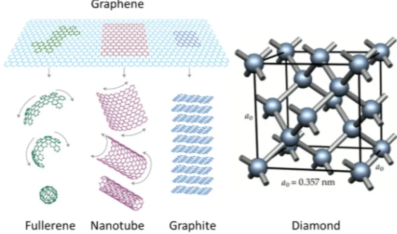
For example, since carbon nanotubes were first synthesized in 1991 [3], carbon allotropes have been the focus of relentless attention from research institutions and semiconductor industries. The versatility of their bonding structure and available dimensionalities (0D fullerenes, 1D carbon nanotubes, 2D graphene, 3D graphite and diamond) leads to a wide range of tunable physical properties for many applications including electronics [4].
In this thesis, we explore the use of two carbon allotropes - textured carbon and graphene - for memory applications, both optically (e.g. for optical disks) and electrically con-trolled (e.g. for computers).
a
Memories: state of the art
a.1
Optical memories
In 1971, Feinleib, Ovshinsky et al. demonstrated reversible phase change in amorphous chalcogenide films (Te81Ge15Sb2S2) [5] using a pulsed argon-ion laser (wavelength 514.5
nm) with pulse durations varying between 1 and 16 µs. Depending on the pulse energy, the structure of the chalcogenide can be changed from amorphous (State 0) to crystalline (State 1) or from crystalline to amorphous (Figure 1.1 (a)). After this first achievement, the technology of laser-induced phase change was continuously developed and adopted by the industry. It eventually led to technologies such as Blu-Ray, the ubiquitous tech-nology for movie recording and viewing (Figure 1.1 (b)).
To increase the density of information that can be recorded on a disk, the surface area of a bit of information must be decreased. This shrinking is achieved by decreasing the
Figure 1.1: Phase change memory technology for electronic and optical memory applications. (a) Switching from a disordered (bottom) to an ordered (top) state in a reversible manner enables to reversibly change the properties of matter, such as its electrical resistivity or optical reflectivity. Reproduced from [6]. (b) A Blu-Ray disk. The phase change is induced by laser pulses (405 nm) of smaller wavelength than those used to induce phase changes in DVDs, resulting in a higher information density.
wavelength of the excitation light, which is the rationale behind the transition from DVD (light wavelength = 650 nm) to Blu-Ray (405 nm).
a.1.1
Mechanism of data storage in optical memories
During the excitation of matter by the laser light, photons are absorbed in matter, lead-ing to the excitation of electrons, which then interact with other free electrons and with lattice vibrations (phonons).
The generation of heat via the transfer of energy from the electrons to the lattice vibra-tions is called "thermalization" [7]. Thermalization occurs on the timescale of picosec-onds (10−12 s, see Figure 1.2). By being heated to higher temperatures, atoms move more freely and take new configurations, possibly leading to phase changes.
As the lattice temperature increases due to the thermalization process, thermal and struc-tural effects such as phase changes or surface damage occur, on timescales on the order of picoseconds to µs (Figure 1.2).
1.1 Optical and electronic memories 27
Figure 1.2: Timescales of various processes occuring during and after laser-matter interactions. Reproduced from [7].
Depending on a number of factors that we will discuss, the resulting matter after cooling may be more amorphous or more crystalline, hence impacting its physical properties (optical, electrical, thermal...) which can later be used as means to "read" the state of a phase change memory device.
a.1.2
Reversible phase change in chalcogenides
Chalcogenides are the chemical compounds used as the memory material in DVD or Blu-Ray disks. They contain at least one chalcogen anion (group 16 elements such as Se and Te) and at least one more electropositive element.
Switching mechanism A simple switching model exists for the reversible phase change in chalcogenides (Figure 1.3) [8, 9].
The important characteristic temperatures of a chalcogenide are its melting temperature Tmand its crystallization temperature Tc(Figure 1.3). The crystallization temperature is
Figure 1.3: Switching mechanism for optical phase change of chalcogenides showing the Write (crystalline to amorphous) and the Erase (amorphous to crystalline) transitions. Both the tempera-ture and the cooling and heating rates are important. For the Write process, matter must be molten (high temperature) then quenched (high cooling rate). For the Erase process, matter must stay long enough at temperatures between the crystallization and melting temperatures. Reproduced from [8].
1.1 Optical and electronic memories 29 crystallize. Hence, there is a "crystallization range of temperatures" between Tcand Tm,
whereby crystallization occurs.
Amorphous to crystalline
During laser annealing, the transition from the amorphous to the crystalline state occurs when the temperature of the material remains between its crystallization temperature Tc
and its melting temperature Tm for a sufficient amount of time (Figure 1.3, right). For
the chalcogenide described in [5] (Te82Ge15Sb2S2), temperatures of Tc≈ 125◦C and Tm≈
380◦C are given for the crystallization and melting temperatures, respectively.
Crystalline to Amorphous: quenching
On the other hand, the transition from the crystalline to the amorphous state occurs through rapid quenching from the liquid state. The temperature must reach higher tem-peratures than the melting point of matter (here 380◦C), resulting in complete fusion,
and then it must decrease to room temperature fast enough to avoid crystallization in the temperature region between the crystalline and melting temperatures Tcand Tm(Figure
1.3, left). For example, in [5], a cooling rate of at least -50◦C/min is a suggested
require-ment to avoid re-crystallization during quenching.
a.1.3
Criteria for phase-change materials for optical recording
To decrease the power consumption (the power consumption is roughly determined by the power of the laser), melting and crystallization temperatures must be as low as possible. However, to provide long-term stability at room and operational temperatures, Tcand Tmmust be much higher than the operational temperature (to avoid unintended
writing). So choosing the right phase change material is a matter of compromise.
Materials other than chalcogenides for which phase-change reversibility has been demon-strated are less performant for an ubiquitous use (e.g. Blu-Ray) because their melting temperature is higher. For example, silicon melts at ≈ 1414◦C, much higher than tel-lurium, which melts at 450◦C.
But amorphous Te is very unstable at room temperature, easily crystallizing [8]. To make the amorphous structure more stable, it can be compounded with other elements such
as Ge or Sb. We recall that the chalcogenide used by Feinleib to demonstrate optical phase-change contained both Te, Ge and Sb (Te81Ge15Sb2S2) [5]. To date, chalcogenides
are still considered one of the best materials for phase change.
a.1.4
Laser annealing of silicon
For the reasons highlighted in the previous section (too high melting temperature), sili-con is not used for optical memory applications. However, there have been many stud-ies on optically induced phase changes in silicon, which are relevant to understand the physics of optically-induced phase changes in materials other than chalcogenides. Moreover, carbon is more similar to silicon than to chalcogenides in terms of struc-ture and physical properties, so silicon laser annealing results provide us with useful information. Both laser-induced crystallization and amorphization of silicon are re-ported.
Contrary to the case of chalcogenides, most reports on silicon crystallization by lasers discuss crystallization directly from the melt [10–18]. We recall that in the case of chalco-genides, the solid material has to remain at temperatures between Tc and Tm (hence
below the melting temperature Tm) long enough for crystallization to occur.
There are two main routes for laser-induced amorphization of silicon: one in which low (but still higher than the melting threshold) energy densities are used (amorphization via quenching) and another in which much higher energy densities are used (amorphization via homogeneous solidification).
Amorphization via quenching The first reports on laser-induced amorphization of sil-icon describe an amorphization mechanism controlled by the rate of solidification of the melt (quenching), expressed in terms of the melt front velocity [11, 12] (threshold veloc-ity ≈ 15 m/s). If the melt front velocveloc-ity is higher than the threshold velocveloc-ity, the matter ends up in an amorphous, metastable state. This is a similar amorphization mechanism as that of chalcogenides (Section a.1.2, page 27).
1.1 Optical and electronic memories 31 The melt front velocity, that control the phase change, is found to depend strongly on the energy density, and also on the wavelength and thickness of the film.
Because higher energy densities lead to higher maximum temperatures, there is more time for the temperature to homogeneize spatially during cooling back down to the so-lidification temperature; hence, at the soso-lidification temperature, the spatial thermal gra-dient is lower for higher energy densities, leading to slower solification velocities and to more time for crystallization processes.
Thus, lower energy densities lead to higher melt front velocities, hence to better amor-phization [11–14, 19, 20], which is why low energy densities just above the melting threshold lead to amorphization.
These studies on laser-induced silicon phase change were so successful that some re-ported limited cycle ability studies [20], providing a proof of principle that silicon could be used as an optical memory material, just like chalcogenides.
Amorphization via homogeneous solidification There are two routes to minimize the crystalline content during cooling of a material from the melt.
In the previous section, we talked about quenching, whereby the temperature drops fast below the crystallization temperature, resulting in the matter retaining its disordered structure. In this case, the success of the amorphization process is impacted by the crys-tallization kinetics of the material, the cryscrys-tallization temperature Tcand the presence
of solid-state catalysts. Solid-state catalysts are remaining solid crystals that can act as a crystallization template for the solidifying liquid [21].
Another route toward minimizing the crystalline content during cooling from the melt is to minimize the amount of such solid catalysts during solidification. Solid crystals that have not melted may act as such catalysts (type 1 catalyst). Moreover, neighboring matter that has just solidified may also act as a crystallization catalyst (type 2 catalyst). A way to minimize the amount of both types of catalysts during solidification is to use very high power densities to increase the maximum temperature reached during the process. It enables full melting, hence removing type 1 catalysts. Moreover, in the molten matter,
the temperature field has more time to homogeneize. If the temperature field is per-fectly homogeneous at the solidification temperature, the material solidifies everywhere simultaneously (homogeneous solidification), hence minimizing the impact of type 2 catalysts.
In [17], Sameshima et al. report reversible phase changes in silicon by means of laser-annealing at high energy densities. After carefully modeling and simulating the tem-perature distribution in the thin film during melting, and by comparing these data with experimental results, they proposed a model for the amorphization process based on homogeneous solidification rather than quenching. They provided precise values de-scribing the environment in which matter solidifies and the consequences of that envi-ronment. They found that, for amorphization to occur:
- all the silicon (resting on a quartz susbtrate) must melt.
- it must remain in the molten state for at least 70 nanoseconds (70x10−9s). - the thermal gradient at the Si/quartz interface must be lower than 1.0*105K/cm.
These requirements are related to the presence of solid catalysts during solidification: all the silicon must be molten so that no remaining solid (type 1 catalyst) is present dur-ing solidification to act as a catalyst; it must remain in the molten state for a significant amount of time so that its temperature homogeneizes spatially, hence providing low thermal gradients. The low thermal gradients are needed to prevent heterogeneous so-lidification, whereby one region solidifies first, hence serving as a crystallization catalyst (type 2 catalyst) for the remaining solidifying matter.
Crystallization Silicon crystallization occurs when the silicon is annealed at an energy density in-between the thresholds for quenching (low energy) and for homoegeneous solid-ification (high energy). All three phase change processes (sorted by increasing energy of the laser pulse: amorphization via quenching, crystallization, amorphization via homo-geneous solidification) start from the melt.
In terms of catalysts, the requirements for crystallization are opposite to those of quench-ing and homogeneous solidification. Crystallization occurs through slow,
heteroge-1.1 Optical and electronic memories 33
Figure 1.4: Optical reflectivity spectra of laser-annealed a-Si:H showing reversible phase changes between an amorphous phase (required energy density = 260 mJ/cm2) and a crystalline phase (required energy density = 220 mJ/cm2). Reproduced from [15].
neous, interface controlled solidification (the interface being the interface between the solid and the liquid, and acting as a type 2 catalyst).
Using the energy thresholds they determined in their studies, Sameshima et al. [15, 17] were able to demonstrate cycling ability (Figure 1.4), with low reported damages.
Summary To summarize this section, current optical memory technologies rely mostly on chalcogenides because their low crystallization and melting temperatures enable low power switching. However, in rough conditions (e.g. for space or defense applications), data may be lost easily because chalcogenides cannot withstand high temperatures. Ma-terials with higher melting points may be used for such niche applications. For example, silicon has been shown to switch reversibly between two crystalline state via single pulse laser annealing.
Figure 1.5: The four main memory technologies are all used in a complementary way. Reproduced from [22].
a.2
Electronic memories
Electronic memories are ubiquitous and essential to our computing and communica-tion systems. Mainstream approaches to memory include hard disk drives, Flash (solid state drives), DRAM and SRAM. They differ by their performances and cost, and all are used in computers at different levels of the computing architecture (Figure 1.5 and Table 1.1).
In this section, we first describe the most common memory devices used for computing and data storage, and then we describe approaches to memory that are still in develop-ment and have the potential to replace or compledevelop-ment current approaches in the near future.
a.2.1
Non-volatile memory: hard disk drives
Hard disk drives are the cheapest (cost per bit) form of memory in the computer archi-tecture. They are used to store the largest amounts of data.
On the other hand, hard disk drives are also the slowest form of memory in the computer architecture (Table 1.1), mainly because moving mechanical parts (a moving head and a spinning disk) are needed.
1.1 Optical and electronic memories 35
Table 1.1: Comparison of the performances of mainstream electronic memory technologies. Data obtained from [23] (all but phase change and metal oxide), [24] (phase change), [25] (Table 4, second column from the right, metal oxide)
Technology
Energy
pJ Read timens Write timens Retention Cycles ION/IOFF
Flash 0.00002 100,000 100,000 years 104 –
DRAM 0.005 10 10 « s > 1016 –
SRAM 0.0005 0.1-0.3 0.1-0.3 = power time 1016 – Hard Disk 1 - 10*109 5 - 8*106 5 - 8*106 years 104 – Phase Change – 60 ns 120 ns > 10 years 109 > 100
Redox 7.5*107 10 ns 10 ns 3hr at 200◦C 1012 > 100
reading consists in characterizing the orientation of the magnetic field generated locally by the material, while writing consists in changing the orientation of that magnetic field. Because the magnetic properties are retained even when the hard disk is not powered, a hard disk is a non-volatile data storage technology.
a.2.2
Non-volatile memory: Flash memories
Flash memory is another form of non-volatile memory. The cost per bit is higher than that of hard disk drives, but Flash memories are still sometimes used to store large amounts of data in solid state drives.
At the bit level, the operation of a Flash memory relies on a floating gate transistor archi-tecture (Figure 1.6). A typical transistor requires only one gate (control gate) that is used to enable or block the flow of current in the channel. In a floating gate transistor, there is an extra (floating) gate between the control gate and the channel: depending on the electric charges it contains, the floating gate may or may not screen (cancel) the electric field provided to the channel by the control gate. Whether the field is screened or not enables to determine the state of the floating gate (charged or un-charged; 0 or 1). Screening is achieved by charging the floating gate, which is a conductive material sand-wiched between the gate and the channel and is electrically insulated from them by two
Figure 1.6: Schematic of a floating-gate-transistor (Flash). Reproduced from http://elec424. rice.edu/gigamesh/blog/index.php?m=01&y=09&d=18&entry=entry090122-181953.
oxide layers (Figure 1.6). Charging the floating gate is done via Fowler-Nordheim tun-neling: when a large electric field is applied accross a thin oxide layer, electrons can "leak" through it due to their wave properties. Thus, writing a Flash memory is done by charging/discharging the floating gate.
As the leakage of charges from the floating gate in the absence of an electric field is low, Flash memory is a non-volatile technology. It can retain its information even when powered off for years (Table 1.1).
Flash memories are used in many applications relying on the easy transport of large amounts of data, such as USB Flash drives or memory sticks for cameras. As their cost goes down with improving technologies, they are now sometimes used as a faster re-placement to hard disk drives in solid state drives.
a.2.3
Volatile memory: dynamic random access memories
Data writing,reading, and transfer rates in non-volatile memories are very slow as com-pared to the operating frequencies of computers. As computers require to constantly store and read data during their calculations, they cannot rely on non-volatile memories to gain from their high operating frequencies.
For this reason, when turned on, computing units communicate mainly with volatile memories, which require constant power to retain information but are considerably faster than non-volatile memories (Table 1.1).
1.1 Optical and electronic memories 37 Each dynamic random access memory (DRAM) cell is composed of a capacitor and a transistor. The information is retained in the capacitor as an electric charge, while the transistor is used to control when the capacitor is read or written. Because the capacitor is constantly leaking its charge, DRAM need to be refreshed constantly, making them more power-hungry than non-volatile memories. They are also more costly, so typically a limited amount of DRAM is present in the computer architecture: only the information used frequently is retained there, while other less accessed informations are stored in the hard disk drive or the solid state drive.
a.2.4
Volatile memory: static random access memories
Static random access memories (SRAM) are the fastest memory devices (Table 1.1). They can operate roughly at the same frequency as the processing units. On the other hand, they are much more costly, as each bit is stored in four to six transistors.
Consequently, there is an even lower (than DRAM) amount of SRAM in the processing unit, and it is typically placed very near the processor, in the "cache". When the pro-cessor is doing operations, it stores the crucial, frequently accessed information in the cache.
SRAM retain their information as long as the power is on, but lose it instantly when it is turned off (volatile).
a.2.5
Non-volatile memory: phase-change
Switching mechanism In 1968, three years before their demonstration of a reversible phase change induced optically [5], Ovshinsky et al. induced reversible phase changes in disordered semiconductors by using electrical pulses [26]. In that case, instead of providing heat via the thermalization of photons, the Joule effect is used.
Except from the heat source, the principle of switching is the same (Figure 1.7 (b)): a high voltage is applied for a short amount of time to melt and quench the material, resulting in the amorphization (RESET, red curve in Figure 1.7 (b)) of the phase change memory
Figure 1.7: Electronic phase change memory. (a) Cross-section of the most common architecture called a "mushroom cell". (b) Switching is achieved by current pulses resulting in heating of the phase change material. Reproduced from [24].
(PCM); a smaller voltage is applied for a longer duration, resulting in the crystallization (SET, blue curve in Figure 1.7 (b)) of the material. The polarization (electric field direc-tion) is not important: PCM devices display a unipolar electrical behavior (Figure 1.8 (b)).
Device architecture The architecture for electronic phase change memories (PCM) com-prises the phase change material (typically a chalcogenide) sandwiched between two electrodes. The bottom electrode is sometimes fabricated smaller than the upper one to provide a localized heating source, hence decreasing the amount of matter to crystal-lize/amorphize at each cycle (Figure 1.7 (a)).
State of the art For the last decades, because silicon-based technologies were deemed more performant for electronic data storage applications, PCM were not used in com-mon computers. However, many researchers and engineers believe that this is about to change [24, 27, 28] as current PCMs are much faster non-volatile memory devices than Flash and hard disk drives (Table 1.1). Recently, very impressive improvements have been demonstrated, with switching speeds faster than 1 ns [29] and energies per bit as small as 100 fJ (20 ns switching speed) [30]. While the metric that keeps semiconductor
1.1 Optical and electronic memories 39 industries away from widely adopting PCM as a replacement to Flash is the cost, it is ac-knowledged that PCM may soon end up being a cheaper technology than Flash memory [31].
a.2.6
Non-volatile memory: binary metal oxide (redox)
Switching mechanism As such, metal oxides are highly insulating (OFF state). How-ever, if a strong electric field is applied to a metal oxide, the oxygen atoms diffuse away from the positive side of the electric field because oxygen is more electronegative than the metal atoms [32]. When the oxygen atoms are repelled (reduction), the remaining atoms are metallic, hence conductive (ON state).
Applying this concept to a metal oxide sandwiched between two electrodes, it is possible to create reduced metal oxide filaments extending from one electrode to the other, hence establishing electrical conduction (OFF to ON).
This process can be reverted (ON to OFF) by applying a negative (opposite direction) electric field, hence attracting the oxygen atoms to the filament location, oxidizing the metal again and restoring the high resistance state. Because electric fields of opposite directions are needed for the full switching cycle of a redox memory, such devices are called bipolar (Figure 1.8 (c)).
It is interesting to note that Redox memories have been described [33] as the fourth missing passive circuit element predicted by Leon Chua in 1971 [34].
Device architecture Devices are fabricated with insulating metal oxide (e.g. TiO2, HfO2)
layers sandwiched between two electrodes (Figure 1.8 (a)). The writing is done by ap-plying voltage pulses of opposite polarities, and the reading is done at low voltages to avoid unintended writing.
State of the art Redox memories are a candidate technology for use as an ubiquitous "universal" memory [35]. They are scalable, offer possibilities for multi-level storage (more than one bit per cell) and endurant. Recently, very high performances have been
Figure 1.8: Redox phase change memory. (a) Cross-section of the most common architecture for redox memories. (b) Unipolar switching characteristic of phase change memories. (c) Bipolar switching characteristic of redox memories. Reproduced from [25].
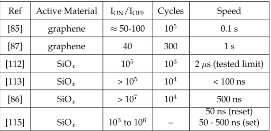
demonstrated with HfOx [36] and TaOx [37] systems, with endurances larger than 1010
(5 ns switching speed), and 1012(< 1 ns switching speed), respectively. The main issue with redox memories for their integration into the computer architecture is their low ION/IOFFcurrent ratio values. For example, in Ref. [25], a table is provided with the best
performances of 11 metal oxide memory devices, and the best performances in terms of ION/IOFFis a ratio above 100.
a.2.7
Non-volatile memory: Magnetoresistive Random Access
Memo-ries
The typical architecture of a Magnetoresistive Random Access Memory (MRAM) is shown in Figure 1.9. It consists in a tunnel junction sandwiched between two magnetic layers: one fixed layer and one free layer. The fixed layer has a fixed magnetization (Left to Right in Figure 1.9), while the magnetization of the free layer can be changed.
The reading of the memory state is done by measuring the amount of current flowing through the cell for a given voltage. If the two magnetic layers are oriented in the same direction (i.e. the free layer magnetization is also oriented from Left to Right in Figure 1.9), the device is in a low resistance state and the bit is "1". On the other hand, if the two magnetic domains are oriented in an anti-parallel manner, very little current flows and
1.1 Optical and electronic memories 41
Figure 1.9: Architecture of a magnetoresistive random access memory
the device is in a high resistance state: the bit is "0".
There are several strategies that can be used to change the orientation of the magnetic domains of the free layer, that is, to "write" the memory. Historically, the first approach that was used was to use the electrical currents running through adjacent conductive lines of memory cells to generate magnetic fields that could be used to switch the de-vice state [38]. Even though this approach is functional, it requires large amounts of currents, making MRAM un-competitive with mainstream approaches such as SRAM or DRAM.
In 1996, it was discovered that the magnetization of a free layer could be controlled by flowing an electrical current through it. This phenomenon is called "spin-transfer torque" and is the basis of the latest generations of MRAM, called spin-transfer torque memories [39].
Currently, thanks to these improvements, MRAM stand as one of the most promising approaches to memory, with properties comparing to the best of SRAM, DRAM and Flash combined [38].
Some reasons for industries not to use MRAM as a mainstream technology yet include the huge investment costs that come with implementing a new technology in a semicon-ductor factory: as long as no company starts investing, it is possible to keep on produc-ing SRAM, DRAM and Flash while remainproduc-ing competitive. On the other hand, startproduc-ing to develop a new approach to mainstream memory is risky, so being the prime mover
is not necessarily deemed as a good approach. Usually, as we will see below with the 3D XPoint technology, INTEL is the prime mover which dictates the pace of develop-ment.
a.2.8
Non-volatile memory: 3D XPoint
In July of 2015, INTEL and Micron announced the development of a new memory tech-nology that they call "3D XPoint". It is said to be non-volatile, to switch 1,000 times faster than Flash memory and to have higher densities than DRAM (Source: http: //www.eetimes.com/document.asp?doc_id=1327289).
Many details have been kept secret, however it is known that this approach does require only one cell per bit with no selection transistor, therefore increasing the memory density. Moreover, the main material is a chalcogenide (Source: http://www.theregister. co.uk/2016/01/29/xpoint_examination/), which is the same material that is used for phase change memories.
Even though phase change memories are one of the most promising approaches to non-volatile memory, both INTEL and Micron have so far denied that the 3D XPoint technol-ogy relies on a phase change mechanism.
Keeping the memory technology secret as long as possible enables both INTEL and Mi-cron to confirm their leadership in the memory industry. As with other developments (e.g. the FINFet transistor), other semiconductor factories will follow the lead of INTEL, which is the company most capable of taking risks and invest heavily in new, disruptive technologies.