HAL Id: tel-02863936
https://pastel.archives-ouvertes.fr/tel-02863936
Submitted on 10 Jun 2020HAL is a multi-disciplinary open access archive for the deposit and dissemination of sci-entific research documents, whether they are pub-lished or not. The documents may come from teaching and research institutions in France or abroad, or from public or private research centers.
L’archive ouverte pluridisciplinaire HAL, est destinée au dépôt et à la diffusion de documents scientifiques de niveau recherche, publiés ou non, émanant des établissements d’enseignement et de recherche français ou étrangers, des laboratoires publics ou privés.
pérovskites hybrides très efficaces
Maria Ulfa
To cite this version:
Maria Ulfa. Nouveaux contacts sélectifs pour des cellules à pérovskites hybrides très efficaces. Autre. Université Paris sciences et lettres, 2019. Français. �NNT : 2019PSLEC005�. �tel-02863936�
Préparée à Chimie ParisTech / Ecole Nationale Supérieure de
Chimie de Paris (ENSCP)
Nouveaux Contacts Sélectifs pour des Cellules à
Pérovskites hybrides très efficaces
(Development of New Selective Contacts for Efficient
Hybrid Perovskite Solar Cells)
Soutenue par
Maria ULFA
Le 3 Avril 2019
Ecole doctorale n° 388
Chimie Physique et Chimie
Analytique de Paris Centre
Spécialité
Chimie Physique
Composition du jury : Pr. Corinne, CHANEAC
Professeure, Sorbonne Université Présidente
Pr. Yvan, BONNASSIEUX
Professeur, Ecole Polytechnique Rapporteur
Dr. Bruno, SCHMALTZ
Maitre de Conférences,
Université de Tours Rapporteur
Pr. Fabrice, GOUBARD
Professeur, Université Cergy-Pontoise Examinateur
Dr. Thierry, PAUPORTÉ
Directeur de Recherche CNRS,
In the name of Allah SWT I dedicate this manucript to all my family, teachers, friends
for their unquestionable support, love, and encouragement May Allah bless you all ☺
Bismillahirrahmanirrahim
Alhamdulillah, all praises to Allah SWT for the strengths and His blessing in completing this thesis. It would also not be possible for me to finish my PhD and to write this doctoral thesis properly without the help and support of many kind people around me. In this occasion, I would like to acknowledge and thank in particular the following people.
A very special acknowledge goes out to the Indonesia Endowment Fund for Education (LPDP) scholarship for the opportunity and for the financial support during this PhD program.
I would like to express my deepest appreciation to my thesis director, Dr. Thierry Pauporté for his guidance and patientless for the last three and half years of my PhD. I am grateful for his endless support and patience in research investigation, writing articles, and correcting my manucripts.
I am also grateful to the following people: Patrick Aschehoug, Sébastien Peralta, Jiawen Liu for their kind help in doing some measurement during my PhD.
I would like to thank Pr. Yvan Bonnassieux and Dr. Bruno Schmaltz for accepting to be my reviewers as well as Pr. Fabrice Goubard and Pr. Corinne Chanéac for being my examiners.
I am deeply grateful for all my colleagues and friends for their help, their support, and for all the great times we shared in the laboratory, and the many scientific discussions. I would like to thank in particular Dr. Yuly Kusumawati, Dr. Jie Zang, Dr. Alexandra Szemjonov, Dr. Sana Koussi, Dr. Pengjiu Wang, Tao Zhu, Daming Zheng, Mariem El Efrit, Maryem, Sana, and many others.
And finally, last but by no means least, I am so grateful for my parents (Hasmi and Ermailis) who raised me with endless love and support, with their unconditional praying for me. For my whole family who always believes in my capability to reach as high as possible in education with all the limitation that I have. And to my husband Yahdi Bin Rus who always courage and accompany me in the whole condition during this PhD. Thanks to all teachers that taught me since I was a child which now bring me to this achievement.
La cellule solaire pérovskite est l’un des sujets de recherche les plus importants dans le monde depuis sa première publication en 2009. Depuis cette date, l’intérêt de la recherche sur les matériaux pérovskites a été étendu à de nombreux types d’applications. Grâce à des études et des recherches intensives, le rendement de conversion de la cellule solaire à pérovskite a été considérablement amélioré jusqu’à 23% dans une courte durée (10 ans). C'est un résultat incroyable par rapport aux cellules solaires au silicium qui ont mis plusieurs décennies à atteindre un rendement aussi élevé. Les recherches portent maintenant sur tous les composants solaires de la pérovskite: le matériau de pérovskite lui-même, la couche de transport d'électrons et de trous ainsi que la structure et les contacts de l'appareil.
Ce travail de thèse visait à réaliser des cellules solaires pérovskites efficaces, stables et reproductibles et à bien comprendre le fonctionnement des cellules. Nous avons commencé par comparer deux techniques différentes de dépôt de MAPI, appelées une étape et deux étapes. En adoptant les deux techniques, nous pourrions atteindre plus de 17% de performance pour CH3NH3PbI3 PSC. Les deux techniques ont ensuite été utilisées pour étudier plusieurs
matériaux de transport de trous. Nous avons étudié le rôle de chaque matériau de transport de trous dans plusieurs structures de pérovskite et les réponses électriques des cellules en réalisant des mesures de spectroscopie d'impédance. Enfin, nous avons concentré notre étude sur la structure plane en utilisant un semi-conducteur à large bande interdite, le SnO2. Une étude
complète a été réalisée, telle que l'épaisseur de la couche de SnO2, le temps et la température
de recuit et la pérovskite pour obtenir un rendement élevé. Enfin, l’étude comparative avec une cellule de TiO2 plane et une cellule de TiO2 mésoporeuse a été réalisée afin de bien comprendre
le fonctionnement des cellules.
Au chapitre 1, nous avons présenté le contexte de la recherche sur les cellules solaires. Tout d'abord, nous avons détaillé le mécanisme de travail des cellules solaires au silicium en expliquant la formation d'une jonction p-n, la formation d'un champ électrique intégré et les processus de séparation de charges dans le dispositif. En outre, nous avons également présenté les nouvelles cellules solaires de pérovskite, en décrivant leur développement et leur évolution au cours des dernières années, y compris les différentes couches fonctionnelles utilisées, la structure des cellules, les techniques de dépôt et d'autres paramètres importants. Nous avons également expliqué le mécanisme de fonctionnement des cellules solaires à pérovskite et enfin,
Au chapitre 2, nous avons présenté une étude comparative de deux techniques différentes de dépôt de CH3NH3PbI3 (1 étape et 2 étapes). Nous avons entièrement caractérisé la couche et les
cellules préparées par les deux techniques. Il était clair que les deux conviennent à la préparation de PSC, qui donne plus de 17% de PCE. Nous avons également profondément caractérisé les réponses électriques de la cellule en mesurant l'impédance et la durée de vie de l'électron par spectroscopie à photoluminescence résolue dans le temps. Nous avons observé que les cellules préparées par 2 étapes n'étaient pas très stables pendant les mesures d'impédance, ce qui rendait leur étude complète difficile.
Au chapitre 3, nous avons étudié en détail les deux principaux types de matériaux de transport de trous: moléculaire et polymère. Nous avons entièrement caractérisé et comparé la réponse électrique des PSC préparés avec la molécule de référence Spiro-OMeTAD HTM et le polymère conducteur poly (3-hexylthiophène-2,5-diyl) (P3HT) choisi pour son cout faible et son efficace. Nous avons également étudié l’effet dopant sur ces HTM. Grâce à la spectroscopie d'impédance, nous avons pu voir clairement que le dopage est vraiment important pour obtenir une efficacité élevée dans la cellule Spiro-OMeTAD alors que l'amélioration était moins significative dans le cas de la cellule P3HT. Nous avons montré que l’oxydation Spiro-OMeTAD par l’additif est importante pour augmenter la conductivité de la couche HTM et diminuer la résistivité interne. De plus, pour les deux HTM, les additifs améliorent l’interface pérovskite / HTM et empêcher la recombinaison des charges. Les dopages ont amélioré l'interface du matériau de transport perovskite / trou pour la cellule P3HT, tout en aidant de manière significative l'oxydation de Spiro-OMeTAD à augmenter sa conductivité et améliorer de la qualité de l'interface perovskite / Spiro-OMeTAD.
Au chapitre 4, nous avons étudié plusieurs nouveaux dérivés du carbazole en tant que matériaux de transport de trous. Ces molécules allaient du grand noyau dendritique B186 aux séries DM et iDM ayant un poids moléculaire inférieur. Premièrement, nous avons incorporé tous ces nouveaux HTM moléculaires dans les PSC en utilisant plusieurs types de structures de pérovskite. Parmi eux, B186 et iDM1 ont montré la plus grande efficacité à 14,59% et 15,04%, respectivement. Nous avons étudié la stabilité des cellules B186 en suivant l'efficacité du dispositif ainsi que le diagramme de réduction des rayons X. Nous avons constaté que le B186 avait une meilleure stabilité que Spiro-OMeTAD. Il est intéressant de noter que les DM1 et
Au chapitre 5, nous avons étudié une structure planaire simple de PSC en incorporant un SnO2
semi-conducteur SnO2 avec une large bande interdite en tant que couche de blocage de trous.
Au début, nous avons complètement étudié l'épaisseur optimale de SnO2, la bonne température
et le temps de recuit, ainsi que le substrat utilisé et sa combinaison avec diverses pérovskites. La condition optimale a été trouvée lorsqu’elle a été préparée en revêtant deux fois une solution aqueuse à 2,35% de colloïdal de SnO2 recuite à basse température (123 ° C). La couche était
exempte de fissures et recouvrait complètement le substrat FTO. Les cellules planaires ont ensuite été préparées en utilisant cette couche combinée avec les pérovskites MAPI (1) -SOF et FAMA. Avec FAMA absorbeur, les dispositifs étaient très efficaces avec un PCE maximum de 18,2% et absence d'hystérésis (6,7% HI) alors qu'avec MAPI (1) -SOF l'efficacité obtenue était de 15,2% avec une hystérésis plus élevée. À des fins de comparaison, nous avons également préparé une cellule solaire plane en pérovskite utilisant une couche de TiO2
pulvérisée en tant que couche de transport d'électrons ainsi que la structure de référence combinant la couche de blocage pulvérisée et la couche mésoporeuse de TiO2. Cela nous a
permis d'obtenir des informations complètes sur le fonctionnement de la cellule.
D'après nos études, il est maintenant clair que la couche de transport d'électrons ou la couche de transport de trous sont très importantes pour obtenir des cellules solaires avec efficacité élevée et stables. Les propriétés de ces couches affectent leur capacité à transporter ou à stocker des supports dans l’ensemble du dispositif. De plus, nous avons illustré la grande importance des interfaces dans les appareils. Une condition optimale pour chaque couche, telle que l'épaisseur et la morphologie, donnait un rendement élevé et des cellules solaires pérovskites stables. Cependant, la préparation de la couche de pérovskite elle-même est également cruciale pour obtenir un rendement élevé. La couche doit contenir le moins de défauts et avoir une cristallinité élevée afin de réduire la possibilité que les processus de recombinaison augmentent l'efficacité. Grâce à notre étude de différents matériaux de transport de trous, nous pouvons affirmer que le Spiro-OMeTAD classique n'est peut-être pas le meilleur matériau de transport de trous pour obtenir une stabilité élevée et une protection contre l'humidité. Nous avons montré qu’il existe plusieurs possibilités de trouver de nouveaux matériaux de transport de trous, qu’ils soient moléculaires, polymères ou inorganiques.Dans des études récentes, nous avons constaté qu'un polymère à base de carbazole présentait une efficacité prometteuse, proche de 17% dans notre groupe. D’ailleurs, l’efficacité de la cellule a augmenté de 18% après 7 semaines de
/ HTM.
En ce qui concerne la couche de transport d'électrons, nous avons montré que la couche d'oxyde de TiO2 présentait certains inconvénients. Récemment, d'autres oxydes, en particulier SnO2, ont
également montré un transfert d'électrons rapide depuis l'absorbeur de pérovskite. Maintenant, il est étudié de manière intensive dans de nombreux groupes. Les avantages du SnO2 ETL
incluent une préparation à basse température, une structure cellulaire simplifiée et une faible hystérésis. Cependant, les performances des cellules SnO2 préparées sont restées inférieures à
aux cellules TiO2 préparées dans le groupe de Pauporté. De plus, nous avons également observé
la qualité de l'interface entre chaque couche afin d'obtenir moins de recombinaison dans les cellules, soit par modification de l'interface avec dépôt de couche mince, soit par examen attentif de chaque couche au cours de la préparation de la cellule.
Nous avons commencé notre étude en utilisant de la perovskite MAPI, qui est moins stable que la perovskite FAMA. Maintenant, dans notre groupe, nous étudions une perovskite à cations multiples additionnée de Cs dans la perovskite FAMA pouvant atteindre 21% de la PCE et ayant une meilleure stabilité. De plus, une pérovskite sans plomb est également une grande opportunité pour les études futures afin de faire face au problème de la toxicité de l'environnement.
Dans le contact métallique, il est possible de changer l’utilisation de l’or avec un autre contact métallique, tel que le noir de carbone, qui peut réduire le coût de fabrication de la cellule.
Sur la base de tous nos résultats et en suivant la tendance des résultats des cellules solaires à la pérovskite, nous croyons que l’efficacité des cellules solaires à pérovskite augmentera continuellement dans l’avenir et il est probable qu’un jour, elles seront commercialisées à grande échelle dans le monde entier.
xii
Table of Contents ... xii
List of Figures ... xv
List of Tables ... xxiii
List of the abbreviations and symbols ... xxvi
General Introduction ... 1
Chapter I :Context ... 3
I.1. Solar Energy ... 3
I.2. Photovoltaics for solar renewable energy conversion ... 4
I.2.1. Silicon solar cells ... 5
I.2.2. Perovskite solar cells ... 8
I.3. Brief description of the perovskite solar cells evolution ... 12
I.4. The working principle of perovskite solar cells ... 19
I.5. Components of perovskite solar cells ... 20
I.5.1. The electron transporting layer ... 20
I.5.2. The perovskite layer ... 21
I.5.3. The hole transporting layer ... 22
I.5.4. The back contact layer ... 24
I.6. The characterizations of perovskite solar cells and of their components ... 25
I.6.1. Material characterizations... 25
I.6.2. Standard solar spectral irradiance ... 25
I.6.3. Current-voltage characteristics ... 27
I.6.4. Quantum efficiency measurement ... 29
I.6.5. Impedance spectroscopy ... 30
Chapter II :Preparation of CH3NH3PbI3 layers and cell performances ... 45
II.1. Introduction ... 45
II.2. Preparation methods of MAPI-based solar cells ... 47
II.2.1. Preparation of the blocking layer (bl-TiO2) ... 47
II.2.2. Preparation of the mesoporous layer (meso- TiO2) ... 49
II.2.3. Preparation of MAPI layers ... 49
II.2.4. Preparation of the hole transporting material layer (HTM) ... 51
II.2.5. Preparation of the back contact ... 51
II.3. Characterization of the MAPI layers prepared by the one-step and the two step methods ... 51
xiii
II.3.3. Optical characterizations ... 53
II.4. Devices performances ... 54
II.5. Aging study of MAPI layers ... 56
II.6. PL spectrum and PL decay study ... 59
II.7. Impedance study of the MAPI solar cells ... 61
II.8. Conclusion ... 67
Chapter III :Molecular and polymeric hole transporting material for high performance perovskite solar cells ... 71
III.1. Introduction ... 71
III.2. Experimental ... 75
III.2.1. Spiro-OMeTAD layer preparation ... 75
III.2.2. P3HT layer preparation ... 76
III.2.3. P3HT spin-coating technique ... 76
III.3. Optical characterizations ... 77
III.4. Perovskite solar cells results ... 78
III.5. Impedance spectroscopy study of perovskite solar cells ... 79
III.6. Photoluminescence (PL) spectrum and decay studies ... 86
III.7. Conclusion ... 88
Chapter IV :New hole transporting materials for perovskite solar cells ... 91
IV.1. Introduction ... 91
IV.2. Experimental ... 93
IV.3. Dendritic carbazole B186 and B74 based HTM ... 93
IV.3.1. Molecular structure and physico-chemical properties of B186 and B74 ... 94
IV.3.2. Solar cells performances ... 95
IV.3.3. Stability tracking of B186- and B74-caped MAPI(1)-SO layers and solar cells .. 98
IV.3.4. Impedance study of B186 and the doping effect ... 100
IV.3.5. Conclusion ... 104
IV.4. DM-based HTM for perovskite solar cells ... 105
IV.4.1. The physico-chemical properties of the DM molecules ... 106
IV.4.2. Performances of solar cells ... 107
IV.4.3. Light soaking effect on perovskite solar cells performances... 109
IV.4.4. Conclusion ... 113
xiv
IV.5.3. Conclusion ... 117
IV.6. General conclusion ... 118
Chapter V :Impact of the oxide layer on the performances of perovskite solar cells .... 121
V.1. Introduction ... 121
V.2. Experimental section ... 123
V.2.1. Preparation of the oxide layers ... 123
V.2.2. Preparation of the perovskite layers ... 123
V.3. Effect of the mesoporous TiO2 layer thickness ... 124
V.4. Optimization of the SnO2 solar cells ... 127
V.4.1. The TCO ... 127
V.4.2. The perovskite ... 130
(a). Comparison of MAPI and FAMA ... 130
(b). Optimization of FAMA in SnO2 cells ... 131
V.4.3. The SnO2 preparation ... 132
(a). The concentration of the SnO2 colloidal solution ... 133
(b). Annealing temperature and time ... 133
(c). Number of coatings ... 135
V.5. Study of planar perovskite solar cells: a comparative study of SnO2 and TiO2 ... 142
V.5.1. Optical characterization ... 142
V.5.2. Structural characterization ... 144
V.5.3. Morphological characterization ... 145
V.5.4. Solar cells ... 146
V.5.5. PL and decay lifetime study ... 148
V.5.6. Impedance study of various perovskite ... 151
V.6. Conclusion ... 156
General conclusion and some future perspectives ... 160
Annex-I ... 164
Annex-II ... 166
xv
Figure 1.1. World energy reserves according to the International Energy Agency (IEA) ... 3
Figure 1.2. Electricity generation by source in the New Policies Scenario, 2000-2040 ... 4
Figure 1.3. Silicon solar cells operating mechanism. (a) Silicon materials doping to form p-type and n-type semiconductor. (b) p-n junction formation. (c) Formation of the built-in electric field. (d) A pair of electron-hole formation after sunlight irradiation. (e) Charge carriers separation and current generation ... 7
Figure 1.4. Schematic of allotropic forms of different types silicon solar cells and their related solar panel module ... 8
Figure 1.5. Perovskite crystal structure ... 9
Figure 1.6. Perovskite solar cell structure ... 10
Figure 1.7. Number of papers on perovskite solar cells published from 2009 to May 15th, 2018 ... 11
Figure 1.8. Chart of the best-cell efficiency of photovoltaic devices recorded by NREL ... 12
Figure 1.9. (a) Schematic drawings for power generation in dye-sensitized solar cells. (b) Schematic drawing for perovskite-sensitized solar cell. (c) Energy diagram for power generation. C.B and V.B are the conduction band and the valence band, respectively. C.E is the counter electrode. QD is quantum dot. (d) Illustration of the incorporating the 2-3 nm sized of perovskite CH3NH3PbI3 nanocrystal to the TiO2 surface. (e) Solar cell J-V curve and EQE of
(d) ... 14
Figure 1.10. Schematic illustration of the charge transfer and charge transport in perovskite-sensitized TiO2 solar cell and a non-injecting Al2O3-based solar cell with the band energy
alignment below (solid circle is electron and open circle is hole) ... 15
Figure 1.11. Schematic drawings for the perovskite preparation with the sequential deposition method ... 16
Figure 1.12. The architecture evolution of PSCs ... 16
Figure 1.13. Fast deposition crystallization (FDC) (left), SEM top-view images from FDC and conventional deposition (right) ... 17
xvi
Figure 1.15. (a) Illustration of a method for fabricating a continuous graded perovskite film by further spin-coating FABr solution in isopropanol on the (FAPbI3)0.85(MAPbBr3)0.15 perovskite film. SEM top-view images of an as-prepared film (b) and a passivated film (c), respectively. Proposed change of cross sectional structures from the as-prepared perovskite film (d) to the passivated film (e) ... 19
Figure 1.16. Schematic representation of the energy levels and electron transfer processes in perovskite solar cells ... 20
Figure 1.17. Molecular structure of (a) Spiro-OMeTAD, (b) P3HT, (c) PTAA, and (d) PEDOT:PSS ... 24
Figure 1.18. Air mass (AM) calculation ... 26
Figure 1.19. Reference solar irradiation spectra according to the standards by American Society for Testing and Materials (ASTM) ... 27
Figure 1.20. Example of current density-voltage (J-V) characteristic curve illuminated by AM1.5G filter spectrum with a power density of 100 mW.cm-2 ... 28
Figure 1.21. Example of EQE spectra and Jph integration curve of high efficiency PSCs ... 30
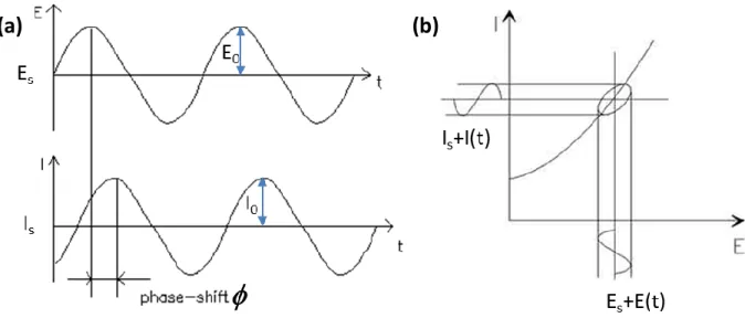
Figure 1.22. (a) Sinusoidal Current Response in a linear system. (b) Steady-state and ac I versus E curves upon impedance measurement ... 31
Figure 1.23. Nyquist impedance plot ... 32
Figure 1.24. (a) Equivalent circuit. (b) Nyquist plot of the spectrum (imaginary as a function of real component). The maximum of the RC-arc takes place at the characteristics angular frequency 0 as indicated. (c, d) Bode representations of the impedance spectrum: (c)
Magnitude versus the frequency and (d) phase versus the frequency. The simulation was conducted from 1 MHz to 1 mHz ... 34
Figure 1.25. (a) Equivalent circuit. (b) Nyquist plot. Bode (c) Magnitude and (d) Phase plot versus the frequency from simulation using the presented values for R1, R2 and CPE. The
exponent of CPE was changed from the ideal case between 1 and 0.5. The red points in the Nyquist plot correspond to the 10000 Hz frequency. The simulation was conducted from 10 MHz to 1 mHz ... 36
xvii
Figure 2.1. Schematic illustration of spray pyrolysis deposition technique ... 48
Figure 2.2. (a-c) SEM top views of the blocking TiO2 layer: (c) SEM zoom view of (a). (d)
Cross-sectional view of the sprayed TiO2 blocking layer ... 48
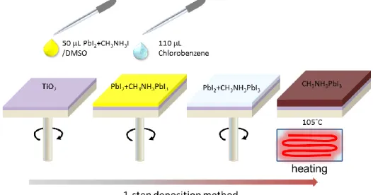
Figure 2.3. Schematic of the two-step sequential deposition method of MAPI layer ... 50
Figure 2.4. Schematic of the one-step deposition method of MAPI layer ... 50
Figure 2.5. Top-view of (a) PbI2 layer and (b,c) MAPI(2) layer. (d) MAPI(1)-SO layer deposited
on TiO2 oxide layer. (e) Cross-sectional view of a complete perovskite solar cell by integrating
a MAPI(1)-SO layer ... 52
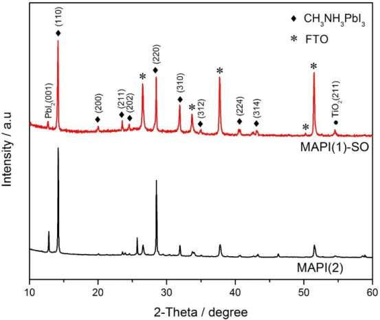
Figure 2.6. XRD patterns of CH3NH3PbI3 perovskite deposited on the TiO2 oxide layer through
one-step and two-step deposition methods ... 53
Figure 2.7. (a) Absorbance and PL spectra of MAPI(1)-SO on glass (red curves) and on FTO/TiO2 (dark blue curves). (c) Absorbance and PL spectra of one-step MAPI. Tauc plots of
(b) MAPI(2) and (d) MAPI(1)-SO deposited on FTO/TiO2 layers ... 54
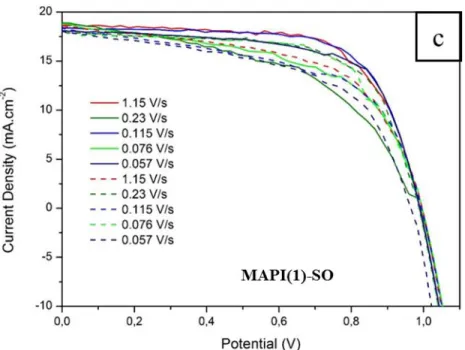
Figure 2.8. J-V curves of the best cells in reverse and forward scan direction (under light) and in dark of: (a) MAPI(1)-SO; (b) MAPI(2). (c) Effect of reverse (full line) and forward (dashed line) scan rate variation on J-V curves measurement of a TiO2/MAPI(1)-SO/Spiro-OMeTAD
solar cell ... 56
Figure 2.9. XRD pattern of; (a,c) MAPI(1)-SO and (b,d) MAPI(2) with and without Spiro-OMeTAD layer deposited on TiO2 layer ... 58
Figure 2.10. (a,b) Photoluminescence spectra of MAPI(1)-SO (a) and MAPI(2) (b) deposited on glass and on TiO2 layers (excitation at 470 nm by a diode laser). (c) Time-correlated
single-photon counting curves of the photoluminescence of the (a) and (b) MAPI samples ... 60
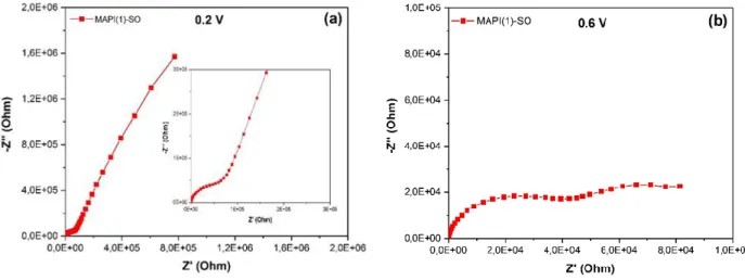
Figure 2.11. Nyquist plots of impedance spectra of PSCs prepared with MAPI(1)-SO perovskite measured under light (a-f) at 0.2V (a,b) and 0.6V (c,d) applied voltages. Zoom view at (e) 0.2V and (f) 0.5V. (g) Three relaxations and (h) two relaxations equivalent electrical circuits ... 62
Figure 2.12. Nyquist plots of impedance spectra of MAPI(1)-SO PSCs measured in the dark at 0.2V (a) and 0.6V (b) applied voltages ... 63
xviii
Figure 2.14. (a) Variation of R2 with Vappl for various perovskite (MAPI(2) is a cell prepared
with a two-step perovskite); (b) The high frequency relaxation time for MAPI(1)-SO cell as a function of the applied voltage ... 65
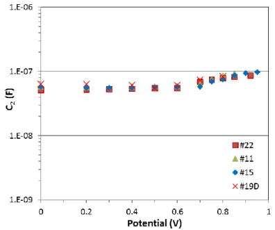
Figure 2.15. (a) Effect of perovskite and light shining on the low frequency C4 parameter. (b)
Low frequency C4 parameter of MAPI(1)-SO cells for hysteresis indexes (HI) of 11%, 22% and
30% ... 66
Figure 2.16. MAPI(1)-SO cell at various voltage (a) low frequency resistance R4 in the dark
(red square) and under light (dark red square).(b) low frequency relaxation time, LF, of the
PSCs measured under light ... 67
Figure 3.1. (a) Molecular structure of Spiro-OMeTAD, (b) P3HT, (c) 4-tert-butylpyridine (tBP) and (d) bis(trifluoromethane)sulfoimide (LiTFSI) ... 75
Figure 3.2. Absorbance curves. (a) Doped and undoped P3HT on glass. Inset: layer picture. (b) Normalized absorbance spectra of doped and undoped P3HT layers on glass. (c) Spiro-OMeTAD undoped on glass and Spiro-Spiro-OMeTAD doped on FTO/Glass (No layer could be deposited directly on glass in this case and the substrate change explain the observed waves above 420 nm) ... 77
Figure 3.3. (a) Exploded schematic view of the perovskite solar cells. (b) Typical J-V curve of solar cells prepared with various doped and undoped P3HT and Spiro-OMeTAD HTM layers (reverse scan) ... 78
Figure 3.4. Impedance spectra Nyquist plots of (a,b) Spiro-based PCS at 0.0V, (c,d) Spiro-based PCS at 0.6V, (e,f) P3HT-based PSC at 0.0V and (g,h) P3HT-based PSC at 0.6V. (b), (d), (f) and (h) are zoom views at high frequencies of (a), (c), (e) and (g) respectively... 80
Figure 3.5. (a) General equivalent electrical circuits used to fit the impedance spectra. (b-d) Electrical equivalent circuits used to fit the Spiro-OMeTAD and P3HT impedance
spectra ... 81
Figure 3.6. (a) High frequency C1 and R1 at various Vappl measured on Spiro-Un cells. (b) Rs
measured at various Vappl for PSCs prepared with Doped Spiro-OMeTAD and P3HT HTMs.
xix
Figure 3.8. Effects of HTM and doping on the variation with Vappl of R4 (a) and C4 (b)
parameters. Effect of Vappl on C4 of (c) pristine and doped Spiro-OMeTAD solar cells and on
L3 of (d) P3HT-Un and P3HT-Co solar cells ... 84
Figure 3.9. PL spectra of (a) SO/Spiro-OMeTAD and (b) SO/P3HT samples. Time-correlated single-photon counting curves of (c) Glass/MAPI(1)-SO/Spiro-OMeTAD and (d) Glass/MAPI(1)-SO/P3HT samples with and without additives . 87
Figure 4.1. Molecular structure of B74 (left) and B186 (right) HTMs ... 94
Figure 4.2. (a) Device structure and (b) energy level alignment of different device components ... 96
Figure 4.3. (a) J-V curves of the best photovoltaic PSCs measured under AM1.5G filtered 100 mW.cm-2 illuminations. (b) EQE curves of PSCs prepared with various HTM. (a) and (b) are
MAPI(1)-SO cells ... 97
Figure 4.4. Evolution of XRD patterns of Glass/FTO/TiO2/MAPI(1)-SO/HTM assemblies
stored under ambient conditions (a) Spiro-OMeTAD, (b) B186, and (c) B74 ... 99
Figure 4.5. Evolution of device performances and J-V curve parameters with storage time for B186 and Spiro-OMeTAD unencapsulated device cells. (a) Normalized VOC; (b) Normalized
JSC; (c) Normalized FF and (d) Normalized PCE ... 100
Figure 4.6. Nyquist plots of impedance spectra of (a,b) of doped and undoped B186 based PSCs. (b) is a zoom view at high frequencies of (a). (c) General equivalent electrical circuit used to fit the impedance spectra. (d,e) Simplified EECs used to fit the impedance spectra of (d) doped B186 and (e) undoped B186 based PSCs ... 102
Figure 4.7. C1 (a) and R1 (b) versus the applied voltage of undoped MAPI(1)-SO/B186 PSCs.
(c) C2 versus the applied voltage of PSCs prepared with B186 in combination of two different
hybrid perovskite absorbers, MAPI(1)-SO and FAMA. (d) SEM cross-sectional view of a B186 based PSC ... 107
Figure 4.8. (a) C4 of doped B186 cells versus applied potential of two different hybrid
perovskite, MAPI(1)-SO and FAMA. (b) R4 of doped B186 cell measured at various potential
xx
Figure 4.10. Energy level alignment of different device components ... 107
Figure 4.11. J-V curves of the best PSCs measured under AM1.5G filtered 100 mW.cm-2 illuminations at reverse scan direction ... 109
Figure 4.12. Light soaking effect on J-V curve of perovskite solar cells prepared with (a) DM1 and (b) DM2 as hole transport material ... 110
Figure 4.13. Effect of scan rate of (a) DM1-based and (b) DM1P-based perovskite solar cells ... 112
Figure 4.14. Molecular structure of iDM1, iDM2, and iDM4 hole transport materials ... 114
Figure 4.15. Best J-V reverse scan curves of the cells combining iDM1 HTM with perovskite absorber ... 116
Figure 4.16. J-V curves of iDM1 measured on both directions (reverse and forward) on (a) MAPI(2), (b) MAPI(1)-SOF, and (c) FAMA ... 117
Figure 5.1. SEM views of TiO2 mesoporous layer prepared using 1:10 (a-b), 1:8 (c-d) and 1:6 (e-f) paste dilutions ... 125
Figure 5.2. J-V curves of 1-step MAPI solar cells prepared with various TiO2 paste dilutions measured at various scan rates in the reverse direction. (a) 1:10 ; (b) 1:8 and (c) 1:6 paste dilutions. The dash lines are the dark currents. (d) Absorbance curve of various TiO2 dilutions ... 126
Figure 5.3. SEM views of FTO (left) and ITO (right) ... 128
Figure 5.4. AFM views of FTO (left) and ITO (right) ... 128
Figure 5.5. Absorbance curves of SnO2 deposited on two different substrates ... 130
Figure 5.6. Perovskite solar cells devices with various perovskite molarities ... 132
Figure 5.7. SEM-top view of various coating number of SnO2 layer deposited on the glass/ITO substrate ... 136
Figure 5.8. AFM images of various coating number of SnO2 layer deposited on the glass/ITO substrate ... 137
xxi
Figure 5.10. AFM images of various coating number of SnO2 layer deposited on the glass/FTO
substrate ... 138
Figure 5.11. (a-d) SEM top view of the bare FTO substrate (a) and after 1 (b), 2 (c) and 4 (d) SnO2 spin-coating step (4.5μm x 3.5μm). (e-h) AFM images of the bare FTO substrate (e) and
after 1 (f), 2 (g) and 4 (h) SnO2 spin-coating steps. (top) : 2μm x 2μm image; (bottom): 800 nm
x 800 nm image (the vertical scale was 300nm for all images). (i) SEM top view of the sprayed TiO2 layer (spr-TiO2) ... 139
Figure 5.12. (a) Absorbance curves of different oxides layer deposited on FTO substrates and (b) Tauc’s plot of spr-TiO2 and spr-TiO2/meso-TiO2 absorbance curves ... 142
Figure 5.13. (a) Absorbance spectra, (b) absorption edge zoom-view and (c) Tauc’s plot of FAMA and MAPI(1)-SOF prepared on various oxide layers ... 143
Figure 5.14. XRD patterns of FAMA deposited on various oxides layer and MAPI on SnO2
layer ... 144
Figure 5.15. 800 nm x 800 nm AFM images of the perovskite layers deposited on the various oxide layers ... 145
Figure 5.16. (a) Planar and (b) mesoscopic PSCs architectures. (c) Cross-sectional SEM view of a planar SnO2/FAMA solar cell. (d) J-V curves under simulated AM 1.5 G illumination of
the best cells with various assemblies. (e) J-V curve of a record SnO2/FAMA solar cell
measured in the reverse (full line) and forward (dashed line) voltage scan directions ... 147
Figure 5.17. (a) Emission spectra of the FAMA layer on glass and supported on various oxide substrates. (b) Time-correlated single-photon counting curves of the photoluminescence of samples (a). (c) PL spectra of MAPI-SOF on glass and on SnO2. (d) Time-correlated
single-photon counting curves of the photoluminescence for MAPI-SOF on glass and on SnO2 contact
layer ... 150
Figure 5.18. (a,b) Nyquist plots of the impedance spectra of cells with various ETL and HP assemblies. (c,d) High frequency zoom views of the spectra. (e,f) Real part of the complex impedance plotted versus the frequency. (g,h) Real part of the complex capacitance plotted
xxii
Full equivalent electrical circuit used to fit the impedance spectra ... 153
Figure 5.19. Variation of the solar cell resistance measured under light at various applied potentials. (a) R2; (b) R3+R4; (c) Variation of the R3 parameter with the applied voltage.... 155
Figure 5.20. Variation of the solar cell capacitances measured under light at various applied potentials. (a) C2; (b) C3; (c) C4. Note that C4 (green open symbol) for SnO2/FAMA is
underestimated due to a very low relaxation frequency IS feature ... 156
Figure AI-1. SEM-view of FAMA on various oxides layer and MAPI(1)-SOF on SnO2 layer
... 164
Figure AII-1. Cyclic voltammogram curves of various coating time of SnO2 layer in an aqueous
solution containing the Fe(CN)63-/4- deposited on (a) ITO substrate- 30 min layer annealing
time ; (b) FTO substrate-30 min layer annealing time; (c) FTO substrate-3h layer annealing time; (d) Curve of (c) with the CV of spr-TiO2 sample ... 166
Figure AII-2. CV-curve characteristics for the FTO/glass substrate before and after different numbers of SnO2 coatings ... 168
xxiii
Table 1.1. Relationship and impedance corresponding to bulk electrical elements. Furthermore, the corresponding electrical equivalent circuit symbols are presented. The graphical representation of the impedance is displayed in the Nyquist plots where Z and Z are the real and imaginary components respectively ... 33
Table 2.1. J-V curve parameters of cells with MAPI(1)-SO and MAPI(2) perovskites ... 55
Table 2.2. Parameters of TCSPC of 1-step and 2-step MAPI deposited on glass and TiO2.
Curves fitted by a bi-exponential decay equation ... 61
Table 3.1. Averaged photovoltaic J-V curve parameters and power conversion efficiencies of PSCs prepared by Drop-Spin and Spin-Drop the P3HT precursor solution. (AM1.5G filtered 100 mW cm-2 illumination) ... 76
Table 3.2. Effect of HTM and additives on the J-V curve parameters (AM1.5 filtered 100 mW.cm-2). Avg: averaged values; Rev: reverse scan direction; For: forward scan direction .. 79 Table 3.3. Parameters of TCSPC of Spiro-OMeTAD and P3HT deposited on MAPI/glass. Curves fitted by a bi-exponential decay equation ... 87
Table 4.1. Comparative thermal, optical and optoelectrochemical properties of carbazole HTMs (B74, B186) and Spiro-OMeTAD ... ...94
Table 4.2. Best and average J-V curve parameters of the solar cells prepared with Spiro-OMeTAD, B74 and B186 HTM. The standard deviations are given in brackets ... ...97
Table 4.3. Thermal, optical and optoelectrochemical properties of DM1, DM2, and DM1P HTMs ... .106
Table 4.4. Best and averaged J-V curve parameters and PCE for cells prepared with MAPI(2) ... .108
Table 4.5a. Light soaking effect on the J-V curve parameters and PCE for cells prepared with DM1/MAPI(2) ... .110
Table 4.5b. Light soaking effect on the J-V curve parameters and PCE for cells prepared with DM2/MAPI(2) ... .111
xxiv
Table 4.7. Thermal, optical and optoelectrochemical properties of iDM1, iDM2, and iDM4 HTMs ... .115
Table 4.8. Best and averaged J-V curve parameters and PCE for iDM1 cells prepared with MAPI(2), MAPI(1)-SOF, and FAMA ... .115
Table 5.1. Effect of mesoporous TiO2 layer thickness on the average J-V curve parameters
(2-step MAPI, AM 1.5 100 mW.cm-2 illumination) ... .126 Table 5.2. Opto-electronic properties of various n-type wide bandgap oxides used in PSCs ... .127
Table 5.3. Summary of J-V parameters of two different TCO substrates ... .129
Table 5.4. J-V parameters of SnO2 solar cells with MAPI(1)-SO and MAPI(1)-SOF... .131
Table 5.5. J-V parameters of SnO2 PSC for various FAMA precursor solution concentrations
... .131
Table 5.6. Summary of J-V parameters of various SnO2 solution ... .133
Table 5.7. Effect of annealing temperature and time of the SnO2 layer on the J-V curve
parameters ... .134
Table 5.8. Roughness parameters measured by AFM for the FTO/glass substrate before and after different numbers of SnO2 coatings ... .140
Table 5.9. Effect of the SnO2 coating numbers on the PSC of J-V parameters ... .140
Table 5.10. Roughness, RMS roughness, grain size and standard deviation (in brackets) of perovskite layers deposited on the various oxides layer ... .145
Table 5.11. Photovoltaic parameters of SnO2-based, TiO2-based planar solar cells and of
meso-TiO2 based solar cells under 100 mW.cm-2 AM 1.5G illumination. The numbers in brackets are
the standard deviations ... .147
Table 5.12. Parameters of PL decays determined from the bi-exponential TCSP curve fitting. Fast and slow lifetimes and relative contributions of the fast and slow components ... .150
xxvi
DSSC Dye-sensitized solar cell
PSC Perovskite solar cell
PCE Power conversion efficiency
Pinc Incident power density
Pmax Maximum output electrical power
Voc Open circuit voltage
Jsc Short circuit photocurrent
FF Fill factor
IPCE Incident photon-to-electron conversion efficiency
EQE External quantum efficiency
IS Impedance spectroscopy
Z Impedance
R Resistance
C Capacitance
bl-TiO2 TiO2 blocking layer
meso-TiO2 TiO2 mesoporous layer
PbI2 Lead iodide
MAI Methylammonium iodide
DMF Dimethylformamide
DMSO Dimethyl sulfoxide
AFM Atomic force microscopy
RMS Root mean square
ETL Electron transport layer
HTM Hole transport layer
TTIP Titanium isopropoxide
LiTFSI Bis(trifluoromethylsulfonyl)imide lithium salt
xxvii
Co(III)complex tris (2-1H-pyrazol-1-yl) - 4-tert-butylpyridine) – cobalt (III) -tris
(bis (trifluoromethylsulfonyl) imide)
CB Chlorobenzene
XRD X-ray diffraction
ACN Acetone nitrile
PL Photoluminescence
TCSPC Time-correlated single-photon counting
RC Relative contribution
τfast Fast decay time
τslow Slow decay time
EEC Equivalent electrical circuit
P3HT Poly(3-hexylthiopene)
FTO Fluorine tin oxide
SEM Scanning electron microscopy
HOMO Highest occupied molecular orbital
LUMO Lowest unoccupied molecular orbital
CB Conduction band
VB Valence band
ITO Indium tin oxide
TCO Transparent conduction oxide
1
Energy is one of the primary needs in modern human life. Fossil fuels, including coals, petroleum and natural gas, have been the main sources of energy since the industrial revolution began in the XVIIIe century. Due to their limitation and the pollution to the environment that they produce, the use of clean and renewable energy sources is essential. Sun is the most abundant source of energy that is renewable and clean. Through a simple photovoltaic device, the energy of the sunlight can be easily converted into the electricity.
Photovoltaic technologies have been developed since long time ago, starting from a silicon solar cell to more recent dye-sensitized solar cells (DSSCs). Surprisingly, a new family of solar cells based on organo-halide perovskite materials, has been found ten years ago. It has shown amazing results in solar cells technology reaching more than 23% of power conversion efficiency lately. Hybrid perovskite materials have a general formula ABX3, contain organic
and inorganic elements and show a suitable bandgap to fully absorb the visible region as well as a small part of the infra-red one. The bandgap of this material can be easily modified by simply changing in their elemental composition.
In this thesis, we have investigated several hole transporting materials (HTM) and we have developed PSC with a planar structure. Chapter 1 is a bibliographic review which describes solar cells from the most popular silicon solar cells to the most recent generation, perovskite solar cells (PSCs). More specifically, we introduce the PSCs evolution in the past few years, including the achievement through the years of various functional layers and cells structure. We also detail the preparation of each layer, the working mechanism of PSCs, as well as the various techniques used in the thesis to characterize the PSCs.
In Chapter 2, we will provide a comparative study of two different MAPI layers prepared by a 1-step and a 2-step deposition technique, as well as the characterization of each layer. Cells performances, PL decay, and impedance study will be used to verify the cells functioning. Both deposition techniques were used to get high efficiency of CH3NH3PbI3 perovskite solar
cells.
In Chapter 3, we compare the integration in the cells of the molecular Spiro-OMeTAD and the conducting polymeric P3HT as HTMs. The effect of the HTM doping on the cell functioning is evaluated through several characterizations. Through PL and PL decay study and impedance spectroscopy (IS) measurements, we deeply analyzed cell parameters that contribute to the cell performances.
2
In Chapter 4, we investigate a group of new carbazole-based HTMs provided by the LPPI laboratory at Cergy-Pontoise. Several kinds of perovskite structure namely, MAPI(1)-SO, MAPI(1)-SOF, MAPI(2), and FAMA have been used to test their performances in PSCs. Moreover, further study such stability and light soaking of several HTMs will also be provide.
In Chapter 5, we have studied a simple planar structure in PSC. These structures are simpler to prepared compared to the mesoscopic ones. SnO2 is a wide bandgap n-type semiconductor
investigated as an electron transport layer. We have studied and optimize several parameters such as the SnO2 layer thickness, the substrate used, the annealing temperature and time, and
the perovskite. In order to fully understand the characteristic of the SnO2 layer in PSC, a
comparative study with TiO2 and a TiO2/meso-TiO2 has been carried out.
3
Context
I.1. Solar energy
Energy is one of the primary needs in modern human life. Fossil fuels, including coals, petroleum and natural gas, have been the main resources of energy since industrial revolution began in the XVIIIe century. The disadvantages of burning fossil fuels have been largely pointed out. First and foremost, it increases the CO2 concentration and is the major reason of environmental damages
due to the increase of global warming. Secondly the burning of low quality of coals releases pollutant to the air such as SO2. These damages will continue due to population growth which
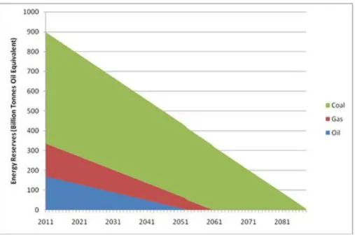
will need more energy in their life. Another fact is that fossil fuels are non-renewable sources of energy which will exhaust in the next decades due to limited resources. According to the International Energy Agency (IEA), the end of the fossil fuel resources is forecasted in less than ten decades. Figure 1.1 shows the prediction limit of these fossil fuels. Oil will run out at about 2052, followed by natural gas in 2061 and coals will be the last resources to be run out in 2088.
Figure 1.1. World energy reserves according to the International Energy Agency (IEA).
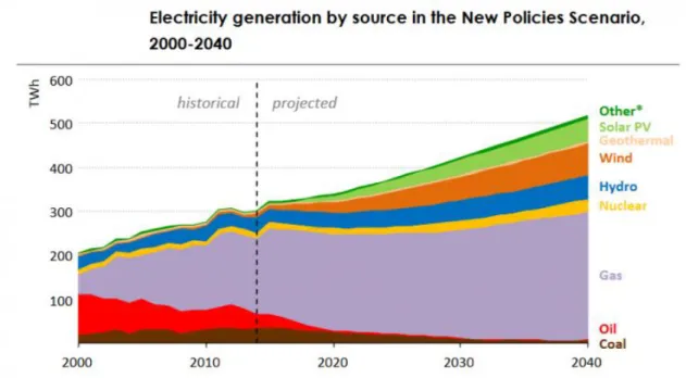
Because of their limitation and pollution issues, people try to find new resources of the energy alternative to fossil fuels that have less or no harmful effects to the environment. Possible green and renewable energies to face those issues are hydroelectric, wind, wave, biomass, geothermal,
4
and photovoltaics. The projection graph can be seen in Figure 1.2. Solar energy is the most abundant resource of energy amongst others with a potential to provide 23.000 TW if it is efficiently harvested.
Figure 1.2. Electricity generation by source in the New Policies Scenario, 2000-2040.
I.2. Photovoltaics for solar renewable energy conversion
Photovoltaic (PV) solar cells are devices that convert light directly into electricity. These devices are one of the most promising alternative to harvest and convert the solar renewable energy nowadays due to its abundance on earth and photoelectric effect [1]. Through a simple combination of n-type and p-type semiconductor (SC) materials, the sunlight radiation can be converted into electricity. Many researchers have developed solar cells technologies in order to fulfil the energy demand. The solar cells are usually classified into three generations. Crystallized silicon-based solar cell is categorized as the first generation, while the thin film solar cells (amorphous silicon, CIGS, CdTe) are categorized as the second generation has and have an average efficiency of 10-15%. Others photovoltaic technologies such as dye-sensitized solar cells (DSSCs), organic photovoltaics (OPVs), quantum dot solar cells (QDSCs), multijunction solar cells and the new emerging perovskite solar cells are categorized as the third generation solar cells. The latters one have demonstrated a power conversion efficiency (PCE) as high as 23.3% within just 9 years of research. Some of these solar cells are briefly explained in the next sections.
5
I.2.1. Silicon solar cells
Among these solar cells technologies, crystallized silicon-based solar cells still dominate the commercial market (about 90%) due to their high efficiency and the high stability with a lifetime that can be as high as 40 years. Silicon solar cells are based on a p-n homojunction. p-type silicon semiconductor is formed when the silicon lattice is doped by boron atom or by another element of the group III of the periodic table. This element traps the free electrons and release free holes leading to an excess of mobile holes. Similarly, by introducing phosphorus or another element of the group V to the silicon lattice, the dopant tends to traps free holes and to release free electrons. It results in a higher concentration of mobile electrons and the SC is n-type doped (Figure 1a). All the charge excesses are free to move randomly. When these two semiconductors are contacted together, a p-n junction is formed. Due to the opposite charges of this junction, the free electrons in n-type semiconductor flow to the p-type to recombine with the free holes. Similarly, holes also flow from the p-type to the n-type (Figure 1b and 1c) and recombine with the electrons. This process continuously occurs until the mobile free carriers exhausted at the p-n junction. It results in a strong built-in electric field (i.e. a space charge region). Under sunlight irradiation, electrons of silicon excited near the space charge region, produce holes and start to move randomly (Figure 1d). The electrons randomly diffuse in the n-type zone while, due to the presence of a strong electric field at the space charge region, the holes drift at the space charge region (Figure 1e) resulting in a separation of the carriers. In the closed-circuit condition, the electrons will travel to the external wire reaching the p-type, where they recombine with the holes, and finally generate a continuous current in the external circuit.
7
Figure 1.3. Silicon solar cells operating mechanism. (a) Silicon materials doping to form p-type and n-type semiconductor. (b) p-n junction formation. (c) Formation of the built-in electric field. (d) Electron-hole pair formation after sunlight irradiation. (e) Charge carriers separation and current generation.
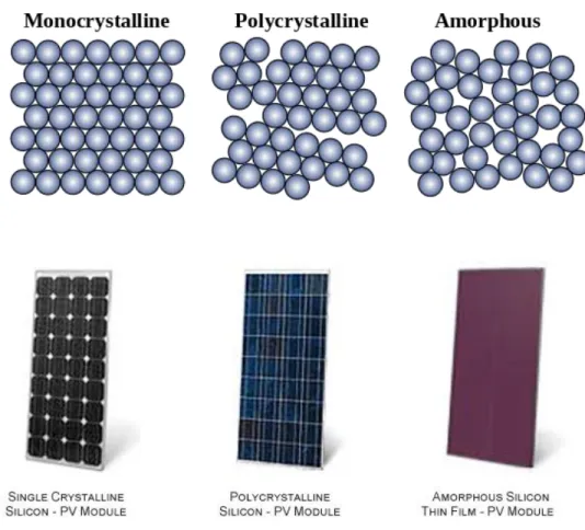
There are three types of silicon-based solar cells: monocrystalline or single crystalline, polycrystalline, and amorphous silicon (Figure 1.4). The single crystalline silicon solar cells are fabricated from very pure single crystalline wafers of silicon. They have a black dark color. They also have been found to be the most robust technology with a lifetime up to 40 years and with most often 25 years warranty (less than 10% of efficiency loss within 25 years). For these reasons, the price of this type silicon solar cells quite high. The polycrystalline silicon solar cells have a better affordable price due to the less difficulties in fabrication process. However, they also have disadvantages such as the need of more installation space due to a less PCE and an efficiency which decreases significantly with the temperature. We can note that the cost of the
8
silicon solar cells has significantly decreased during the last years. Finally, amorphous silicon is used in thin film technology solar cells. It can be deposited on various substrates such as glass, metal, and plastic. Amorphous silicon is a more absorbing SC than crystallized silicon due to a direct bandgap transition while the latter is an indirect bandgap sSC.
Figure 1.4. Schematic of allotropic forms of different types silicon solar cells and their related solar panel module.
I.2.2. Perovskite solar cells
Historically, the first natural perovskite was discovered by the German mineralogist Gustrav Rose in 1839 in the Ural mountain. It was named perovskite in honor of the Russian mineralogist Lev Alexeïevich Perovsky.
Three-dimensional (3D) perovskites have the general formula ABX3 that adopt the same crystal
structure as CaTiO3 where A and B are cations of different atomic radii (A larger than B) and X
9
sharing BX6 octahedra and the A-cation is located at the interstitial space in the
three-dimensional structure formed by the eight adjacent octahedra (Figure 1.5).
Figure 1.5. Perovskite crystal structure.
In organic-inorganic hybrid perovskite (HP) solar cells, the A cation is typically an organic aliphatic amine such as methylammonium (CH3NH3+) and formamidinium ((NH2)2CH+) or a
monovalent alkali (Li+, Na+, K+, Rb+, Cs+). B is a metallic cation such as Pb2+, Sn2+ or Ge2+ from group IV and X is a halogen anion which can be Cl-, Br-, or I-. Since a perovskite formed by three main elements, the limits on ionic sizes of each component then so-called the Goldschmidt tolerance factor for a particular perovskite has been defined as:
𝑡 = 𝑟𝐴+ 𝑟𝑥 √2(𝑟𝐵+ 𝑟𝑥)
(1.1)
Where rA, rB, and rX are the ionic radii of the A, B, and X components of the perovskite lattice. t
= 1 correspond to a perfectly packed structure, and it can be varied only in a restricted range (0.8 to 1) [2]. For most perovskites it has been stated to lie between 0.8 and 0.9 [3].
The organic-inorganic hybrid perovskite materials have amazing electrical and optical properties. First, it has larger Bohr radius [4], a high dielectric constant, and a weak exciton binding energy (<10 meV) [5]–[7] that permit a fast dissociation of the exciton at room temperature, secondly, it has a long carrier diffusion length (up to 1 m for thin films) [8] and high carrier diffusion velocity that prevent a quick recombination. Thirdly, the iodide compounds have an appropriate band-gap of about 1.5-1.6 eV that can absorb efficiently the UV-Vis spectral range[4]. These
10
properties can be tuned by varying the A, B, and X ions [9] and the appropriate selection of different cations and organic anions will change the band-gap of the material [10].
In PSCs, the absorber is typically sandwiched between an electron transporting layer and a hole transporting layer. The photo-generated charge carriers diffuse to the selective contacts. The electrons are then injected into the electron transporting layer and the holes into the hole transporting layer. Due to the charge separation and collection a current is generated. Classically, Au (or Ag) acts as the back contact while FTO (or ITO) is the front contact of the device. Figure 1.6 shows the typical direct structure of a PSC.
Figure 1.6. Perovskite solar cell structure.
Due to the unique properties of the perovskite materials, they have become the most promising candidates for high-efficiency and low-cost solar cells. From the finding of Kojima et al. in 2009 who first used the CH3NH3PbI3 and CH3NH3PbBr3 perovskites as a sensitizer in dye-sensitized
solar cells [11], this subject has attracted a large attention of the solar cells research community and has become one a very hot research topic these last years. This is illustrated by the number of papers annually published on the topic (Figure 1.7) and it has resulted in an amazing efficiency of 23.3 % reached within a short time as shown in the NREL chart (Figure 1.8).
11
Figure 1.7. Number of papers on perovskite solar cells published from 2009 to April 23th, 2019 (source:
Web of Science Database, accessed in 23 April 2019).
4 5 9 13 60 492 1351 2338 3120 3684 1019 0 500 1000 1500 2000 2500 3000 3500 4000 N u mb e r o f Pub lic ati o n Year of Publication W E B O F S C I E N C E D ATA B A S E K E Y W O R D S E A R C H : " P E R O V S K I T E S O L A R C E L L S " * L I M I T E D F R O M 2 0 0 9 - 2 3 A P R I L 2 0 1 9 2009 2010 2011 2012 2013 2014 2015 2016 2017 2018 2019
12
Figure 1.8. Chart of the best-cell efficiency of photovoltaic devices recorded by NREL [NREL chart: https://www.nrel.gov/pv/cell-efficiency.html].
The classical methylammonium lead triiodide (CH3NH3PbI3) is the most used compound in
perovskite solar cells (PSCs) studies. However, recently, multiple cation perovskite containing a mixed organic and inorganic cation (CH3NH3+ + (NH2)2CH+ + Cs+) and mixed anions (Cl- and
Br-) showed better performances as well as better stability.
I.3. Brief description of the perovskite solar cells evolution
The perovskite solar cells (PSCs) originated from the dye-sensitized solar cells (DSSCs). The organometal halide perovskites (HPs) was firstly used as sensitizers in a photo-electrochemical cells where CH3NH3PbBr3 and CH3NH3PbI3 were tested as quantum dots in replacement of a dye
[11].
In DSSCs, a mesoporous thick layer of a wide bandgap semiconductor (typically TiO2 anatase) is
sensitized to solar light by the adsorption of a monolayer of a dye (D). Excitons are generated in the dyes by the transition of electrons from the HOMO level to the HUMO levels (D*). The
13
electrons are then quickly injected from the photo-excited dye to TiO2 and the dye cation is
produced (D+). This is followed by the regeneration (reduction) of the oxidized dye by iodide in solution which is oxidized in tri-iodide (I3-). I3- is finally regenerated at the cell counter-electrode
by reduction and the current flow in the external circuit. The general functioning mechanism is summarized in Figure 1.9a. One can note that the liquid electrolyte that contains the redox couple can be replaced by a molecular p-type semiconductor but the PCE is less in this case.
The initial PCE was 3.81% for the first perovskite sensitized solar cells published by Kojima et al., prepared by spin-coating the perovskite precursor solution on top of a mesoporous TiO2 film
on FTO glass substrate. In these cells, like in DSSCs the holes were transported by a redox couple dissolved in an organic liquid electrolyte. The power generation mechanism was described as similar to that in a DSSC as shown in Figure 1.9b and 1.9c. Park et al. followed this finding by a significant improvement of PCE to 6.5% by incorporating the 2-3 nm sized of perovskite CH3NH3PbI3 nanocrystal to the TiO2 surface [12]. However, the cells were not stables due to the
14
Figure 1.9. (a) Schematic drawings for power generation in dye-sensitized solar cells. (b) Schematic drawing for perovskite-sensitized solar cell. (c) Energy diagram for power generation. C.B and V.B are the conduction band and the valence band, respectively. C.E is the counter electrode. QD is quantum dot
[11]. (d) Illustration of the incorporating the 2-3 nm sized of perovskite CH3NH3PbI3 nanocrystal to the
TiO2 surface. (e) Solar cell J-V curve and EQE of (d) [12, p. 5].
Liquid-based PSCs have durability problem due to the liquid electrolyte in the device. On May 2012, Snaith et al. submitted a paper in which an all-solid-state perovskite-sensitized solar cells was presented which was based on meso-superstructured HPs and Spiro-OMeTAD as the hole transporting material instead of an iodine/iodide-based electrolyte [13]. The active layer was CH3NH3PbI2Cl that originated from dissolving PbCl2 and CH3NH3I in DMF solvent. It resulted
in a PCE of 7.6% using mesoporous TiO2 and 10.9% for Al2O3-based devices (Figure 1.2). Park
et al. also submitted the solid-state PSCs two months later, which exhibited 9.7% of PCE by using CH3NH3PbI3 as the absorber [14]. They assumed a power generation mechanism similar to
that in DSSCs, the electrons being injected from perovskite to the conduction band of TiO2. The
chloride-containing perovskite proposed by Snaith et al. did not rely on the sensitization mechanism while the latter one reported by Park et al. assumed opposite. These two main ideas became the sources of PSC studies [15].
15
Figure 1.10. Schematic illustration of the charge transfer and charge transport in perovskite-sensitized TiO2 solar cells and in non-injecting Al2O3-based solar cells with the band energy alignment (the solid
circle is an electron and the open circle is a hole) [13].
Grätzel et al. [16] reported a 15% of PCE in 2013 for a perovskite layer prepared by a sequential deposition technique reported previously by Mitzi et al [17]. The PbI2 layer was first deposited on
the TiO2 layer and then immersed into a CH3NH3I solution in order to be converted into
perovskite within the nanoporous host (see Figure 1.11). This deposition technique was claimed to permit a better control of the perovskite morphology and to increase the reproducibility.
16
Figure 1.11. Schematic drawings for the perovskite preparation with the sequential deposition method [16].
The researchers also considered the use of a mesoporous oxide layer. On June 2013, Snaith et al. submitted two papers without incorporating the mesoporous layer (planar hetero-junction) PSCs which showed 11.4% [18] of PCE when the perovskite was prepared by a solution process (the mesoporous-based cells procedure) and 15.4% [19] of PCE for the perovskite prepared by dual-source vapour deposition process. These results showed that the mesoporous oxide layer is not necessary to produce efficient devices. Finally, the architecture evolution of perovskite solar cells is summarized in Figure 1.12.
Figure 1.12. The architecture evolution of PSCs [20], [21].
Inverted architecture of PSCs has also been studied. The PCE was only 3.9% PCE in the first publication [22]. However, later, their PCE was significantly improved with four papers which
17
reported efficiencies of 16.3% [23], 16.5% [24], 17.1% [25] and 17.7% [26]. Mostly, the common architecture used in PSCs are the mesoporous-based and planar-based PSCs.
A significant improvement in the efficiency (19.3%) was reported by Yang et al. and published online in August 2014 by adapting the planar-heterojunction architecture [27]. They carried out the delicate control of the carrier dynamics throughout the device by incorporating yttrium-doped TiO2 as the electron transport layer. The experiment was conducted by solution-based at low
temperature and in the air. In May 2014, Cheng et al. published a dripping anti-solvent method to promote fast-crystallization of the perovskite layer. By using chlorobenzene, a densely packed crystalline perovskite was obtained and led to a 16.2% PCE [28]. This preparation method became one of the most used in the studies on PSCs then. The solvent engineering was also introduced by Han et al. [29] in 2014. DMSO used as a solvent instead of DMF showed smaller distribution of particle sizes and resulted in less deviation in the cells efficiency.
Figure 1.13. Fast deposition crystallization (FDC) (left), SEM top-view images from FDC and conventional deposition (right) [28].
Another remarkable progress was the appearance of the mixed cation perovskite reported by Seok et al. in 2015 [30]. Mixing formamidinium (FA) and methylammonium (MA) formed (FAPbI3)0.85(MAPbBr3)0.15 perovskite structure exhibited 18.4% of the efficiency. Since then,
many PSCs papers have adopted this new perovskite structure and it resulted in an efficiency of more than 20%, also in our group (Pengjiu Wang, “Design of oxide contacts and mixed cation hybrid perovskite for highly efficient solar cells”, PhD thesis, 2018). Salida et al. then showed that the solar cell efficiency could be increased by adding small amounts of Cs+ [31] and/or Rb+ ions [32].
18
On February 2015, Seok et al. [33] reported the intramolecular change during the preparation of perovskite layers by replacing the DMSO molecules intercalated in PbI2 by external FAIs to form
highly efficient FAPbI3-based PSCs with a certified PCEs exceeding 20%. Park et al. reported the
use of DMSO adducts in preparation of MAPbI3 perovskite’s precursor that lead to a 19.7% PCE
[34].
Figure 1.14. Illustration of intramolecular change introduced by Seok et al [33].
On August 2015, Nazeeruddin et al. reported the advantage of using a PbI2-rich precursor
solution which cells exhibited better performances compared to the stoichiometric case with a PCE at 19.09% [35]. Interestingly, Park’s group found the opposite result, they reported the better performances for an excess of MAI [36]. The investigation of the un-stoichiometric case was also studied for mixed cation (FAPbI3)1-x(MAPbBr3)x. Several papers such as Nazeeruddin,
Grätzel, and Hagfeldt et al. reported that changing the PbI2/FAI ratio resulted 20.8% of PCE for
1.05:1 PbI2/FAI ratio [37], Seok et al. added 5.7 mol % of PbI2 to (FAPbI3)0.85(MAPbBr3)0.15 and
the cells exhibited a 20.1% PCE [38]. The Grätzel group reported the treatment of the samples with vacuum after the spin-coating process and it resulted in a 20.5% PCE for a 0.16 cm2 mask and 20.3% for a 1.00 cm2 mask [28]. An improvement was observed by modifying the perovskite surface using a FABr solution spin-coated on top of (FAPbI3)0.85(MAPbBr3)0.15 perovskite layer.
19
Figure 1.15. (a) Illustration of a method for fabricating a continuous graded perovskite film by further spin-coating FABr solution in isopropanol on the (FAPbI3)0.85(MAPbBr3)0.15 perovskite film. SEM top-view images of an as-prepared film (b) and a passivated film (c), respectively. Proposed change of
cross sectional structures from the as-prepared perovskite film (d) to the passivated film (e) [39].
The iodide-management was proposed by Seok et al., in mixed cation perovskite for performance improvement. They prepared the perovskite layer by using the 2-step deposition technique. The PbI2 and PbBr2 mixed solution in DMF/DMSO was first spin-coated on TiO2 layer, then the
mixture FAI and MABr dissolved in isopropyl alcohol was spin coated. By using this technique they could report a 22.6% PCE and a NREL certified 22.1% PCE [40]. Adding 5% cesium into mixed cation perovskite resulted a 21.1% PCE [31] and by incorporating Rb+ to the perovskites, Saliba et al. showed the 21.8% PCE for RbCsFAMA system [32]. Using the latter composition, they also reported in 2016 the used of CuSCN inorganic hole transporting material which exhibited a 20.4% PCE while the Spiro-OMeTAD-based cells resulted in 20.8% PCE [41]. Incorporating Rb and Cselements made a reproducible perovskite layer. Segawa et al. also reported recently a potassium-doped perovskite which showed over 20% of PCE without hysteresis [42]. Finally, the highest record PCE for perovskite solar cells until today is 23.3% (shown by NREL chart in Figure 1.8) which is superior to other thin film solar cell technologies.
I.4. The working principle of perovskite solar cells
Figure 1.16 shows the energy levels and mechanism of charge-transfer processes in a TiO2/perovskite/HTM cell. The process started by (1) the photo-excitation of the perovskite
absorber and creation of electron-hole pairs after sunlight irradiation. Charge separation then occurred through two possible primary reactions: (2) photo-generated electrons in the perovskite are injected to the TiO2, and (3) the holes transfer to the HTM layer. Finally, both electrons and
20
holes are collected to the front and back contact, respectively, in order to generate the photocurrent. However, there several undesirable processes happen in PSC such as; (4) recombination of the photo-generated charge carriers either radiative or non-radiative as a result of exciton annihilation, as well as recombination of the charge carriers at the three interfaces: (5) TiO2/perovskite, (6) perovskite/HTM, and (7) TiO2/HTM. The latter may occur only when the
perovskite layer is not fully covering. Based on these processes, it is clear that the charge recombination processes (4-7) should occurr at a slower time scale than charge generation, separation, and extraction processes (1-3) to get high PCE of PSCs.
Figure 1.16. Schematic representation of the energy levels and electron transfer processes in perovskite solar cells [43].
I.5. Components of perovskite solar cells
I.5.1. The electron transporting layer
The role of the electron transporting layer (ETL) is to extract electron carrier from the perovskite and ensures its transport to the front contact of the cell. This layer is typically made of an oxide semiconductor with a wide band gap. This layer prevents the direct contact between the transparent conducting oxide (TCO) and the perovskite by well covering the TCO surface. In order to get high performance perovskite solar cells, the ETL must meet several criteria: (a) a good optical transmittance in the visible range; (b) proper band energy levels compared to the
![Figure 1.16. Schematic representation of the energy levels and electron transfer processes in perovskite solar cells [43]](https://thumb-eu.123doks.com/thumbv2/123doknet/2720809.64443/46.918.157.760.393.736/figure-schematic-representation-energy-electron-transfer-processes-perovskite.webp)