HAL Id: pastel-01006041
https://pastel.archives-ouvertes.fr/pastel-01006041
Submitted on 13 Jun 2014
HAL is a multi-disciplinary open access
archive for the deposit and dissemination of sci-entific research documents, whether they are pub-lished or not. The documents may come from teaching and research institutions in France or abroad, or from public or private research centers.
L’archive ouverte pluridisciplinaire HAL, est destinée au dépôt et à la diffusion de documents scientifiques de niveau recherche, publiés ou non, émanant des établissements d’enseignement et de recherche français ou étrangers, des laboratoires publics ou privés.
Study of the physical mechanisms involved in the
femtosecond laser optical breakdown of dielectric
materials
Alexandros Mouskeftaras
To cite this version:
Alexandros Mouskeftaras. Study of the physical mechanisms involved in the femtosecond laser optical breakdown of dielectric materials. Plasma Physics [physics.plasm-ph]. Ecole Polytechnique X, 2013. English. �pastel-01006041�
Thèse présentée pour obtenir le grade de
DOCTEUR DE L’ECOLE POLYTECHNIQUE
Spécialité: Physique
par
ALEXANDROS MOUSKEFTARAS
Sujet de la thèse :
Study of the physical mechanisms involved in the
femtosecond laser optical breakdown of dielectric
materials
Soutenue le 11 Février 2013 devant le jury composé de :
Dr. Marc SENTIS
Président
Prof. Bärbel RETHFELD
Rapporteur
Dr. Razvan STOIAN
Rapporteur
Prof. Manuel JOFFRE
Examinateur
Dr. Stéphane GUIZARD
Directeur de thèse
Remerciements
D’abord, je souhaite exprimer ma gratitude aux personnes qui ont permis la r´ealisation de ce travail de th`ese. Cette derni`ere a ´et´e realis´ee au laboratoire des solides irradi´es (LSI) de l’Ecole Polytechnique d’Octobre 2009 au Janvier 2013. Je tiens `a remercier Martine SOYER en tant que directrice du laboratoire pour m’avoir accueilli au sein de cela.
Ensuite, je souhaite remercier Prof. B¨arbel RETHFELD et Dr. Razvan STOIAN pour avoir accept´e de se charger de la lourde tache de rapporter cette th`ese ainsi que pour leurs remarques qui ont permis d’am´eliorer la qualit´e de ce manuscrit. Je remercie ´egalement Dr. Marc SENTIS et Prof. Manuel JOFFRE d’avoir accept´e de faire partie de mon jury. Je suis tr`es reconnaissant `a l’ensemble des membres du jury pour leur flexibilit´e et leur bonne volont´e, notamment quand il a fallu changer de salle en pleine s´eance des questions.
Je remercie tr`es profondement mon directeur de th`ese Dr. St´ephane GUIZARD pour m’avoir guid´e tout au long de cette aventure scientifique. J’ai eu la chance de travailler avec un scientifique d’une qualit´e exceptionnelle. J’ai encore plus de chance d’avoir ´etabli une tr`es belle amiti´e avec St´ephane qui perdurera, je suis sˆur, dans le temps.
Durant ma th`ese, j’ai eu la chance ´egalement de travailler avec Dr. Sergei KLI-MENTOV qui m’a accompagn´e lors de nombreuses exp´eriences d’interferometrie fr´equentielle et de spectroscopie de pohto´electrons. J’ai particuli`erement appreci´e nos discussions scientifiques et son goˆut pour la science. Je n’oublie pas Dr. Nikita FEDOROV, qui a partag´e ses comp´etences en tant qu’exp´erimentateur d’exception lors de ma premi`ere ann´ee de th`ese.
Ce travail doit beaucoup aux personnes qui se sont occup´e du bon fonction-nement de la chaˆıne Laser Ultra-Court Accordable ( LUCA), au comissariat `a en-ergie atomique (CEA) du centre Saclay. Je souhaite remercier notamment Olivier GOBERT, Michel PERDRIX, Fabien LEPETIT et Delphine JOURDAIN.
Je souhaite ´egalement remercier Dr. Ghita GEOFFROY, directrice adjointe au Centre Lasers Intenses et Applications (CELIA) de Bordeaux, pour sa collab-oration lors des exp´eriences de spectroscopie de photoelectrons.
4
jusqu’`a l`a. Je pense notamment `a Olivier (le Rouennais) et Olivier (le Breton) qui m’ont beaucoup soutenu lors de ma premi`ere ann´ee en France et aussi par la suite, pendant toutes mes ann´ees universitaires, Keven qui a toujours ´et´e un ami dont j’´etais fier et Debajyoti de partager une belle amiti´e. Je suis tr`es reconnaissant `a Yorgo pour avoir ´et´e ami et p`ere adoptif.
Abstract
We have carried out detailed time resolved experimental studies of the mechanism of electron excitation-relaxation, when an ultrashort (60 fs -1 ps) laser (ultravio-let (400 nm for this thesis) (UV) and infrared (800 nm for this thesis) (IR)) pulse interacts with a wide band gap dielectric material. The studies cover a range of dif-ferent dielectric materials and the investigated regimes span from non-destructive ionization of the material at the low power end (∼ TW/cm2) to ablative domain
at a higher laser power (∼ 10 TW/cm2). This gives fundamental insight into the
understanding of the laser damaging process taking place under our irradiation conditions. The usage of time-resolved spectral interferometry technique allows to directly measure the electron density of the irradiated material under differ-ent excitation conditions and hence leads to quantification of the process. The measurements, carried out at the optical breakdown threshold utilizing different pulse durations, raise questions regarding the usage of critical excitation density as a universal ablation criterion. A new criterion related to the exchanged energy is proposed. Additionally, the use of an experimental setup implementing a dou-ble pump pulse allows the identification of different excitation mechanisms taking place at time scales of the order of the pulse duration used. Electronic avalanche is observed in some materials (SiO2, NaCl) while this is not the case for others
(Al2O3, NaCl). These differences are discussed in detail. Next, we measure the
energy spectrum of excited electrons with a complementary technique: the pho-toemission spectroscopy. These results allow us on one hand to show a crossed effect between the two pump pulses and on the other hand to measure electron relaxation characteristic times, as a function of their kinetic energy. Finally, a morphological study of craters resulting from ablation in the case of a single pulse has been carried out for different irradiation parameters: number of shots, energy and pulse duration. This work has been extended to the case of double pulse damage, with the relative delay being the studied parameter.
Contents
Introduction 19
1 Theoretical description of the short pulsed laser-dielectric
inter-action 25
1.1 Introduction . . . 26
1.2 Excitation processes in dielectric solids . . . 29
1.2.1 Muliphoton ionization . . . 31
1.2.2 Defect-assisted ionization . . . 33
1.2.3 Tunnelling ionization . . . 34
1.2.4 Forest fire . . . 34
1.2.5 Electron ”heating” and collisional ionization . . . 35
1.3 Energy relaxation mechanisms . . . 39
1.4 Conduction band depopulation . . . 42
1.5 Theoretical models . . . 43
1.6 Damaging criteria . . . 44
2 Experimental investigation of electron excitation and recombina-tion processes 45 2.1 Introduction . . . 46 2.2 Interferometry . . . 49 2.2.1 Goal . . . 49 2.2.2 Spatial interferometry . . . 49 2.2.3 Temporal interferometry . . . 50 2.2.4 Frequency-domain interferometry . . . 53
2.2.5 Extraction of the phase shift . . . 55
2.3 Experimental setup . . . 58
2.3.1 Overview . . . 58
2.3.2 Setup discussion and optimization . . . 60
2.3.3 Final version of the experimental setup . . . 68
2.4 Theoretical considerations . . . 70
2.4.1 Different contributions to the phase shift . . . 70 3
4 CONTENTS
2.4.2 Relation between excitation density and phase shift . . . 80
2.5 Experimental results . . . 83
2.5.1 Choice of irradiation parameters . . . 83
2.5.2 Long electron lifetime materials . . . 84
2.5.3 Short electron lifetime materials . . . 93
2.5.4 Optical damage and criteria . . . 105
2.6 Conclusion . . . 113
3 Experimental study of electron kinetic energy distribution in the CB 117 3.1 Introduction . . . 118
3.2 Principle of the photoemission spectroscopy . . . 119
3.2.1 Single pulse . . . 119
3.2.2 Double pulse . . . 121
3.3 Drawbacks and consequences . . . 123
3.3.1 Electron mean free path . . . 123
3.3.2 Space charge . . . 123
3.3.3 Surface charge formation . . . 125
3.3.4 Surface contamination . . . 127 3.4 Preliminary discussion . . . 128 3.4.1 Photionization . . . 128 3.4.2 Electron heating . . . 128 3.4.3 Relaxation dynamics . . . 131 3.5 Experimental setup . . . 133
3.6 Experimental results and discussion . . . 135
3.7 Conclusion . . . 140
4 Damage morphology studies in SiO2 141 4.1 Introduction . . . 142
4.2 Experiment . . . 144
4.3 Results . . . 146
4.3.1 Pulse duration study . . . 146
4.3.2 Number of shots . . . 151
4.3.3 Pulse delay study . . . 161
4.4 Conclusion . . . 169 General conclusion & Perspectives 171
List of Figures
1 a scanning electron microscopy (SEM) of a row of holes in Corning 0211 glass. b, c Examples of nanometer-scale holes. The hole in c is 15 nm in diameter. Figure from [47]. . . 20 2 Profile of an array of channels drilled with identical 0.70 µJ energy
per pulse and beam position such that channel length is 10 µm and diameter 230 nm. The pitch is 1.6 µm. White circles indicate chan-nel positions. Inset shows post-processed surface for an additional sample closer to threshold with pitch 800 nm. Scale bar is 200 nm. Figure from [8]. . . 21 3 Colouring resulting from laser micro-inscription on stainless steel,
performed at Laboratoire Hubert Curien (LaHC). . . 22 1.1 The fermi function f(E ) is the probability that an energy level E is
filled with an electron; 1-f(E ) is the probability of occupancy by a hole in the valence band. At T = 0 K, f(E )=1 for E < EF; i.e.,
there are no electrons in the conduction band and no holes in the valence band. Figure from [82]. . . 27 1.2 Band structure of a perfect solid crystal and possible electronic
tran-sitions by absorption of optical radiation. On the left: 1-photon transitions. On the right: multiphoton transitions. EF is the Fermi
level. Figure from [67]. . . 28 1.3 Possible excitation mechanisms involved in the interaction of a wide
band-gap dielectric with an ultrashort pulse. Ec, Ev and Eg stand
for conduction, valence and band gap energy respectively. Electrons (e) and holes (h) are represented. Red straight arrows stand for IR photons.See text for more details. . . 30
6 LIST OF FIGURES 1.4 The electrostatic potential seen by the electron, in the presence of
an external electric field is represented in black solid lines (in form of wells). Dotted lines represent the atomic potential while blue solid lines the external potential related to the applied field. In the case of low-to-moderate electric field strength multiphoton ab-sorption dominates (left part of the figure, red arrows correspond to absorption of laser light photons). When the laser intensity is of the order of the atomic unit, then the overall potential is modified and tunnelling (violet arrow) is possible, assisted by photon absorption. Horizontal lines represent the vacuum level. . . 35 1.5 Indirect transitions in a phonon-assisted photon absorption scheme
in a crystalline solid. Two types are represented (intraband and interband). figure from [67]. . . 36 1.6 Illustration of electron ”heating” by inverse bremsstrahlung,
eventu-ally followed by impact ionization and resulting in electronic avalanche, in a crystalline solid. . . 37 1.7 On the left part, semi-empirical scattering rates in SiO2 at 300 K as
a function of the electron kinetic energy. On the right, momentum relaxation rates (panel a) and energy relaxation rates (panel b) in SiO2 versus electron kinetic energy. The solid curve is the
acoustic-phonon scattering rate, the dot-dashed curve is the 153-meV longi-tudinal optical (LO)-phonon scattering rate and the dotted curve is the 63-meV LO-phonon scattering rate. Figure from [3]. . . 40 2.1 Phase shift as a function of laser intensity measured in Al2O3. The
pump wavelength is 800 nm and the duration is 60 fs. The line is indicating an I6 dependence law. The arrow and empty circle
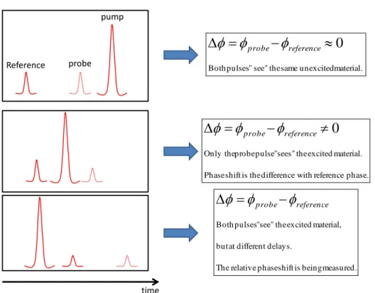
indicate the breakdown threshold. Figure from [72]. . . 47 2.2 Young’s double slit experiment, on the right part an object of
ho-mogeneous refractive index n has been added in the path of one ray, a is the separation between the slits, D the distance between the slits plane and the observation plane, S is the light source, S1, S2
are the two slits, M is a point on the observation plane and x is the shift of the fringe pattern due to the phase object . . . 50 2.3 A possible experimental setup for temporal interferometry is
pre-sented. Moving one mirror of the Michelson interferometer changes the optical path (delay) between the pulses. . . 51 2.4 The simulated interference is plotted. Blue solid curve correspond
to the case where reference and probe pulse go through the same medium. Green, dotted curve correspond to a π/2 phase shift, in-duced by a pump pulse preceding the probe pulse. . . 52
LIST OF FIGURES 7 2.5 A possible experimental setup for spectral interferometry is
pre-sented. The positions of the mirrors are fixed, thus defining the
time delay between the two pulses. . . 54
2.6 The simulated interference is plotted. Blue solid curve correspond to the case where reference and probe pulse go through the same medium. Green, dotted curve correspond to a π/2 phase shift, in-duced by a pump pulse preceding the probe pulse. . . 55
2.7 The simulated inverse Fourier transform of the spectrum. . . 56
2.8 The experimental setup in its simplest version. . . 58
2.9 Spectrometer front view. . . 59
2.10 charged coupled device (CCD) camera view inside the spectrometer. On the left is the interference pattern observed without pump pulse and on the right with a pump pulse in the center. The displacement of the fringes in the center is signature of the phase shift change. . . 60
2.11 Phase shift as a function of the transverse coordinate of the beam r, for three pump-probe delays. From top to bottom different con-tributions encountered are : Kerr effect, free carrier generation and trapped carrier formation respectively (see section 2.4.1 for more details) The three different regions to be integrated are illustrated, with light grey being the integration over the ground level and yel-low the actual measured signal. . . 61
2.12 Illustration of the approach used to separate the different excitation mechanisms. . . 62
2.13 Experimental result of the phase shift as a function of an IR pump-probe delay in SrTiO. The positive and negative peaks represent the beginning and the end of the absolute phase shift scan respectively. 64 2.14 Illustration of the different cases distinguished depending on the pump-probe delay. Probe and reference pulse delay is fixed. . . 65
2.15 Illustration of the Mach-Zender interferometer. . . 65
2.16 Principle of using a Michelson interferometer behind the sample for spectral interferometry. . . 66
2.17 Illustration of the two possible configurations for the pump and the probe. The probe beam is represented by a single line representing the ray entering the monochromator’s entrance slit. Refraction has been neglected and a top hat profile for the pump beam has been employed for the figure. . . 67
8 LIST OF FIGURES 2.18 Optimized version of the initial experimental setup.The almost collinear
configuration is being represented, with the perpendicular one be-ing possible as well. Double pump and probe experiment is possible with variable radiation parameters.There is possibility of translating the sample in all three directions. . . 68 2.19 Phase shift measurements as a function of the pump-probe delay,
for two different materials with a 400 nm pump. . . 71 2.20 Long scan in Al2O3 with a 400 nm pump. Fluence is 1.28 J/cm2
and pulse duration = 60 fs. . . 72 2.21 Phase shift along the beam’s radial coordinate. Different curves
stand for different pump-probe delays. Gaussian fit is used to de-termine the beam’s spot size. . . 73 2.22 Free electron contribution to the real part of the refractive index in
α − SiO2. On the left, the two curves are plotted for two different
collision frequencies: ωc = 1f s −1
. On the right, the same is done for two effective masses:m∗
= m0. In all cases, the contribution is
negative at moderate densities (before reaching Nc). Black curve
represents the unperturbed refractive index. . . 74 2.23 Comparison between two models in α − SiO2 : one considering
valence band (VB) depletion and the other one not. Black curve is the unperturbed refractive index. . . 77 2.24 Refractive index dependence on temperature in Al2O3. Arrows
point out melting and boiling points. Black lines delimit the do-main at which Zouboulis et al.[105] have developed the model. . . . 78 2.25 Plotted phase shift experienced by a 800 nm pulse through
trans-mission in a medium of excitation density N. Two curves are plotted : one considering a collisional rate and one neglecting collisions. . . 79 2.26 Illustration of the phase shift dependence on excitation density.
De-lay between pump and probe considered is of 50 fs (no trapping occurs). Simulation parameters are : ωc=1 f s−1,λprobe = 800nm,
m∗
= m0 and n0 = 1.54 (Sα − iO2).Two probed lengths are plotted
: 10 µm and 100 µm. No other contribution to the phase shift has been taken into account (moderate densities assumption). . . 81 2.27 Fluence at damage threshold (DTH) for a sequence of a IR pulse
(300 fs duration) and a UV (60 fs duration) fluence, at fixed delay between them (UV pulse first). Three different materials are repre-sented : Al2O3, MgO and α − SiO2. A vertical line is plotted at 70%
of the single pulse damage threshold; UV or IR pulse alone (SDTH) with the UV pulse alone. . . 85
LIST OF FIGURES 9 2.28 Phase shift in a double pump pulse scheme as a function of
pump-probe delay measured for different IR fluencies in two different crys-tals. Phase shift for 400 nm alone is in blue circles, for 800 nm in red squares and for both beams together (7 ps interval, UV first) in black diamonds. On the left, the results for Al2O3 and on the right
for MgO. UV (50 fs duration) fluence is : 2 J/cm2 for Al
2O3 and
1.3 J/cm2 for MgO. IR (50 fs duration) fluence is increased from
top to bottom. combined pulse damage threshold: IR fluence for a UV-IR sequence (CDTH) is 5 J/cm2 for Al
2O3 and 3.5 J/cm2 for
MgO. . . 86 2.29 Phase shift in a double pump pulse scheme as a function of
pump-probe delay, for two different IR (10 ps duration) fluencies measured in Al2O3. Phase shift for 400 nm alone is in blue circles, for 800 nm
in red squares and for both beams together (5 ps interval, UV first) in black diamonds. UV (50 fs duration) fluence is 2 J/cm2. . . 88
2.30 Fitting the experimental results from figure 2.29 using a quadratic recombination model (equation 2.46). Fitting the 400 nm + 800 nm signal requires multiplying the electron velocity v by ten. . . 89 2.31 Phase shift in a double pump scheme as a function of the
pump-probe delay measured in MgO. Fluencies are 0.71 J/cm2 for UV
(50 fs pulse duration) and 5.72 J/cm2 for IR (1 ps pulse duration).
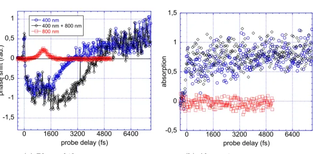
Pulse delay is 15 ps, UV arriving first. . . 90 2.32 Phase shift and probe absorption in a double pulse scheme as a
func-tion of the pump-probe delay in Al2O3. Signal for 400 nm pulse (50
fs duration) alone is in blue circles, for 800 nm in red squares and for both beams together (UV first) in black diamonds. (a): Fluencies are 1.3 J/cm2for UV and 4.14 J/cm2 for IR (1 ps duration). UV-IR
delay is 2 ps. Pump-probe geometry is co-linear.(b): Fluencies are 1.85 J/cm2 for UV and 7 J/cm2 for IR (2 ps duration). UV-IR delay
is 3 ps. Pump-probe geometry is perpendicular. . . 91 2.33 Phase shift and probe absorption measurement, in same
experimen-tal conditions, in MgO with a single IR pump pulse (1 ps duration) as a function of the pump-probe delay. . . 92 2.34 Double pump phase shift (and the corresponding probe absorption)
measurement in α − SiO2 as a function of the pump-probe delay,
for different IR (350 fs duration) fluencies. Signal for 400 nm pulse alone is in blue circles, for 800 nm in red squares and for both beams together (400 fs delay, UV first) in black diamonds. UV (50 fs duration) fluence is 0.7 J/cm2. CDTH fluence is 1.66 J/cm2. . . . 94
10 LIST OF FIGURES 2.35 Illustration of the competition between trapping and heating
pro-cesses in α − SiO2. Initially, electrons are promoted in the
conduc-tion band (CB) by multiphoton absorpconduc-tion. Then, these carriers are trapped by self-trapped exciton (STE)’s within 300 fs. . . 95 2.36 Double pump phase shift (and the corresponding probe absorption)
measurement in NaCl as a function of the pump-probe delay, for different IR (300 fs duration) fluencies. Signal for 400 nm pulse alone is in blue circles, for 800 nm in red squares and for both beams together (500 fs delay, UV first) in black diamonds. UV (50 fs duration) fluence is 0.4 J/cm2. CDTH fluence is 0.36 J/cm2. . . . 97
2.37 Double pump phase shift (and the corresponding probe absorption) measurement in KBr as a function of the pump-probe delay. UV (50 fs duration) fluence is 0.12 J/cm2 and IR (500 fs duration) is
0.32 J/cm2. Delay is 1.3 ps (UV first). . . 98
2.38 Double pump phase shift measurement in α − SiO2 as a function of
the pump-probe delay, for different IR fluencies. Signal for 400 nm pulse alone is in blue circles, for 800 nm in red squares and for both beams together (500 fs delay, UV first) in black diamonds. UV (50 fs duration) fluence is 0.35 J/cm2 and IR (300 fs duration) is 0.32
J/cm2. . . 99
2.39 Double pump phase shift (and the corresponding probe absorption) measurement in α − SiO2 as a function of the pump-probe delay,
for different UV-IR pump delays. Signal for 400 nm pulse alone is in blue circles and for both beams together in black diamonds. UV (50 fs duration) fluence is 0.4 J/cm2 and IR (350 fs duration) is 1
J/cm2. IR pulse is being delayed from top to bottom and here the
the -275 fs to 200 fs delays are presented. . . 100 2.40 Longer UV-IR delays are being explored. Experimental parameters
are the same as in 2.39 . . . 101 2.41 Phase shift measured in double pulse scheme for two pump-probe
delays: right after IR pulse (200 fs) and 1 ps after UV pulse, as a function of the pump pulses relative delay. Data is taken from figures 2.39 and 2.40. . . 102
LIST OF FIGURES 11 2.42 SiO2: Left column: Phase shift in a double pump pulse scheme, at a
given UV pump-probe delay, as a function of the UV-IR pump delay, for different IR fluencies. First a conventional UV pump-probe scan is presented (top figure) to illustrate the UV pump-probe delay for which the phase shift variation is measured (black diamonds) as a function of the UV-IR pump delay. The same results at a different scale are presented on the right column. UV (50 fs duration) fluence is 1.12 J/cm2. Pump-probe geometry is co-linear. . . 104
2.43 SiO2: Phase shift in a double pump pulse scheme, at a given UV
pump-probe delay, as a function of the UV-IR pump delay, for dif-ferent IR fluencies. First a conventional UV pump-probe scan is presented (top figure) to illustrate the UV pump-probe delay for which the phase shift variation is measured (black diamonds) as a function of the UV-IR pump delay. The same results at a different scale are presented on the right column. UV (50 fs duration) fluence is 1.12 J/cm2. Pump-probe geometry is perpendicular. . . 106
2.44 NaCl: Phase shift in a double pump pulse scheme, at a given UV pump-probe delay, as a function of the UV-IR pump delay, for dif-ferent fluencies. First a conventional UV pump-probe scan is pre-sented (top figure) to illustrate the UV pump-probe delay for which the phase shift variation is measured (black diamonds) as a func-tion of the UV-IR pump delay. UV (50 fs durafunc-tion) fluence is 0.41 J/cm2. IR (300 fs duration) fluence is 0.47 J/cm2. Pump-probe
geometry is co-linear. . . 107 2.45 Maximum phase shift (single pump pulse) at damage threshold (in
absolute value) along with absorption are measured with respect to the IR pump pulse duration. . . 108 2.46 Damage thresholds on the surface as a function of UV-IR pump
delay, for different IR pulse durations. UV is a short pulse (50 fs) constantly maintained at 70% of SDTH. Two different IR polariza-tions have been tested : UV and IR polarizapolariza-tions are parallel (blue line) and UV polarization is perpendicular to IR (red line). On the left, we present the results for Al2O3 and on the right for MgO. . . 109
2.47 SiO2: Maximum phase shift (single pump pulse) at damage
thresh-old (in absolute value) along with laser intensity are measured with respect to the IR pump pulse duration. . . 111
12 LIST OF FIGURES 2.48 Damage thresholds on the surface of α − SiO2 as a function of
UV-IR pump delay, for different UV-IR pulse durations. UV is a short pulse (50 fs) constantly maintained at 70% of the SDTH. Two different IR polarizations have been tested : UV and IR parallel plotted on the blue line and UV perpendicular to IR on the red line. . . 112 3.1 Schematic description of photoelectric effect in a solid, near the
surface. Red arrow represents incoming photon with energy ¯hω. Different energy levels are represented : energies of initial and fi-nal electron state Ei and Ef respectively, binding energy Eb, work
function φ, Fermi level EF, vacuum level Evac and electron kinetic
energy Ec. Only electrons with an energy greater than Evac can
escape the medium. . . 119 3.2 Three step model after Spicer. Detection of a photoelectron involves
excitation, transport to the surface and emission. . . 120 3.3 Summary of the different processes taking place in a double pulse
scheme. An IR (often stretched) pulse and a UV short pulse are used. Three situations are illustrated : IR pulse arrive before, at coincidence and after UV pulse. The mechanisms are numbered from 1 to 5 as follows : 1 and 2 for IR and UV multiphoton ion-ization respectively, 3 for electron ”heating”, 4 is the sum of two independent multiphoton ionizations (UV and IR) and 5 is impact ionization. A crossed photon excitation (UV+IR) is represented at coincidence as well. List is not exhaustive. . . 122 3.4 Mean free electron path as a function of its kinetic energy in bulk
material. Metal case is represented but trend is similar in inorganic solids (such as α − SiO2). A universal law is observed for all solids. 124
3.5 Different tensions are applied on a α − SiO2 sample to observe if a
space charge effect exists. Spectra are translated for comparison. A 800 nm pulse, 28 fs pulse duration has been used as excitation source.125 3.6 Thermal emission spectrum of an α − SiO2sample heated up at 400
◦
C. No laser is present and therefore signal is due to electrons being emitted by the electrode used to heat the sample. Fluctuations at the peak are present while the electron maximum energy is constant from one shot to another. . . 126 3.7 Photoelectron spectra on α − SiO2 excited by 40 fs pulses at 800
nm for different intensities. Figure from [102]. . . 129 3.8 Photoemission spectra for different pulse (800 nm) durations at
LIST OF FIGURES 13 3.9 Surface, corresponding to the total number of emitted electrons,
and maximum kinetic energy measured for different pulse durations in α − SiO2. Processing of data from figure 3.8. . . 131
3.10 Experimental setup used to perform single or double pulse photoe-mission spectroscopy, see text for details. . . 133 3.11 Photoemission signal as a function of the electron kinetic energy in
α − SiO2. UV: 30 fs pulse duration, 0.01 J/cm2 fluence); IR: 30 fs,
0.29 J/cm2) and UV along with IR at temporal coincidence, below
DTH. . . 135 3.12 Relaxation time of electrons depending on their kinetic energy in
α − SiO2. Irradiation parameters are the same as in 3.11. . . 136
3.13 Schematic description of the interaction process of a train of pulses with a dielectric. Electrons are promoted in the conduction band by multiphoton absorption and they are acquiring further energy by inverse Bremsstrahlung. Relaxation processes may include impact ionization or other inelastic collision mechanisms (electron-phonon). 137 3.14 Electron counts versus electron kinetic energy in α − SiO2. IR: 200
fs duration, 2.2 J/cm2; UV: 30 fs duration, 0.03 J/cm2 and UV
along with IR at zero time delay, below DTH. . . 138 3.15 Photoemission signal as a function of the pulse UV-IR pulse delay at
a given electron kinetic energy, in α − SiO2. Negative delay values
correspond to IR arriving first. Irradiation parameters are the same as in 3.14. . . 139 4.1 SEM image of SiO2irradiated with a single IR pulse. Pulse duration
is τ =60 fs and fluence at F = 1.2 J/cm2 (corresponding to 150% of
the SDTH). . . 147 4.2 SEM image of SiO2 irradiated with a single IR pulse. Two different
pulse durations: 1 and 2 ps with different fluencies are exposed. . . 149 4.3 SEM image of SiO2 irradiated with a single IR pulse. Two different
pulse durations: 5 and 10 ps with different fluencies are exposed. . . 150 4.4 SEM image of SiO2 irradiated with N= 2 and N= 5 shots of IR
pulses (τ = 300 fs), at a fluence of 5.6 J/cm2. . . 152
4.5 SEM image of SiO2 irradiated with N = 10 and N = 20 shots of IR
pulses (τ = 300 fs), at a fluence of 5.6 J/cm2. . . 153
4.6 SEM image of SiO2 irradiated with N= 2 and N= 3 shots of UV
pulses (τ = 60 fs), at a fluence of 3.1 J/cm2. . . 154
4.7 SEM image of SiO2 irradiated with N = 5 and N = 10 shots of UV
pulses (τ = 60 fs), at a fluence of 3.1 J/cm2. . . 155
4.8 SEM image of SiO2 irradiated with N=20 shots of UV pulses (τ =
14 LIST OF FIGURES 4.9 Damaged area as a function of the number of shots for a UV pulse,
of duration τ = 60 fs, at a fluence of 3.1 J/cm2 . . . 157
4.10 SEM image of SiO2 irradiated with N= 5, 10, 20 double-pulse (UV
and IR) sequences of fixed delay [∆t = 200 fs] at corresponding flu-encies of 1.8 J/cm2for UV(τ = 60 fs) and 0.8 J/cm2 for IR(τ = 300 fs).159
4.11 Damaged area as a function of the number of shots for a double-pulse sequence of a UV double-pulse of duration τ =60fs, at a fluence of 1.8 J/cm2 and an IR pulse, of duration τ =300fs, at a fluence of
0.8 J/cm2. The same result with UV pulse alone (F = 3.1 J/cm2)
is plotted along. . . 160 4.12 SEM images of SiO2irradiated with N = 10 UV and IR shots (upper
and lower part of the figure respectively). . . 162 4.13 SEM images of SiO2 irradiated with 3 double-pulse (UV and IR)
sequences of varying delays [∆t = −667 fs to 1.3 ps] at correspond-ing fluencies of 1.9 J/cm2 for UV(τ = 60 fs) and 2 J/cm2 for
IR(τ = 300 fs). Lower and higher delay for which damaging was observed is represented. Notice the change in scale between the images. . . 163 4.14 Damaged area as a function of the pulse delay (black full circles) for
N=3. Single pulse cases are plotted along (blue line for UV and red line for IR). The electron lifetime ”window” in CB is represented in the hatched area. . . 164 4.15 SEM images of SiO2 irradiated with 5 double-pulse (UV and IR)
sequences of varying delays [∆t = −667fs to 1.3 ps] at correspond-ing fluencies of 1.9 J/cm2 for UV(τ = 60 fs) and 2 J/cm2 for
IR(τ = 300 fs). Lower and higher delay for which damaging was observed is represented. Notice the change in scale between the images. . . 165 4.16 Damaged area as a function of the pulse delay (black full circles) for
N=5. Single pulse cases are plotted along (blue line for UV and red line for IR). The electron lifetime ”window” in CB is represented in the hatched area. . . 166 4.17 SEM images of SiO2 irradiated with 10 double-pulse (UV and IR)
sequences of varying delays [∆t = t = −667 fs to 1.3 ps] at cor-responding fluencies of 1.9 J/cm2 for UV(τ = 60 fs) and 2 J/cm2
for IR(τ = 300 fs). Lower and higher delay for which damaging was observed is represented. Notice the change in scale between the images. . . 167 4.18 Magnified view of 4.17b. . . 168
LIST OF FIGURES 15 4.19 Damaged area as a function of the pulse delay (black full circles) for
N=10. Single pulse cases are plotted along (blue line for UV and red line for IR). The electron lifetime ”window” in CB is represented in the hatched area. . . 168 4.20 Damaged area as a function of the pulse delay (black full circles)
16 LIST OF FIGURES
Acronyms
UV ultraviolet (400 nm for this thesis) . . . 1
IR infrared (800 nm for this thesis) . . . 1
MPI multiphoton ionization . . . 29
TI tunnelling ionization . . . 29
AI avalanche ionization . . . 62
FDI frequency domain interferometry . . . 63
CB conduction band . . . 10
VB valence band . . . 8
STE self-trapped exciton . . . 10
EM electromagnetic . . . 79
VUV vacuum ultraviolet . . . 119
DTH damage threshold . . . 8
SDTH single pulse damage threshold; UV or IR pulse alone. . . .8
CDTH combined pulse damage threshold: IR fluence for a UV-IR sequence . . . 9
LIST OF FIGURES 17 HSFL high spatial frequency LIPSS . . . 142 LSFL low spatial frequency LIPSS. . . .142 SEM scanning electron microscopy. . . .5 BBO barium borate . . . 133 PCI polarization contrast intensity . . . 169 NBOHC non-bridging oxygen-hole center . . . 42 PES photoemission spectroscopy . . . 117 DIT direct interbranch transition . . . 121 PE photoemission . . . 123 CELIA centre lasers intenses et applications . . . 129 CCD charged coupled device. . . .7 AC alternating current . . . 32 DC direct current. . . .26 LO longitudinal optical . . . 6 NBOHC non bridging oxygen hole center . . . 42
18 LIST OF FIGURES SFI Strong-Field ionization . . . 33 OFI optical Field ionization . . . 34
Introduction
It all started somewhere in 1960 with the first and successful laser emission from a ruby crystal by Theodore Maiman. Shortly after (1961), the second harmonic generation from this rubidium laser has been observed in quartz [28] Soon (in 1967) this spatially confined energy source (continuous wave), provided a direc-tional emission, found its applications in the industry with the first laser cut event on stainless steel, using a 300 W, CO2 laser. Later and with further confinement
of the energy in time (pulsed-laser), a wider range of applications was made possi-ble while the spatial and temporal coherence of this source offered a new powerful tool for diagnostics. The laser-matter interaction field was making its debuts. Fur-ther development of the laser sources, involving new wavelengths and higher peak power helped materialize previously predicted theoretical considerations based on nonlinear interaction research.
By the end of the 80s, it was assumed that everything was known about mode-locked femtosecond lasers. Then, starting in 1990 and using Ti:Sapphire lasers, 160 fs [45] and 60 fs [90] pulses have been successfully produced. This along with the chirped pulse amplification (CPA,[93]) technique combined together, made possible the delivery of mJ laser pulses, with pulse durations below 100 fs. Optimal temporal resolution and energy localization had been achieved providing both the tool for extreme stimulation and subsequent response study of the materials.
Over the years, a large variety of applications for ultrashort pulses (∼ fs − ps) have made their appearance exploiting different aspects of this irradiation. Sub-micron machining has been reported as early as 1995 by Pronko [70] on a silver film, where a nano-hole with a depth of 52 nm has been produced. However, although early investigations focused on metals, ablation is possible in transparent dielectric materials as well, in bulk or on the surface. The longitudinal confinement, a consequence of using fs or ps laser pulses, has been studied in sapphire by S. Guizard et al. [39]. In parallel, the lateral confinement of a gaussian laser pulse along with the precise energy threshold in this time scale revealed sub-micron features. These involve 15 nm holes in fused silica [47] (see figure 1) and the laser drilling of nano-channels in thick glass (∼ 400 nm in diameter and ∼ 43 µm deep) [8]. The latter may be of great interest for photonics and/or
20 CHAPTER 0. INTRODUCTION fluidics. Finally, ultrashort laser pulse machining may be used for processing fine structures in a variety of materials [64]. These applications involve fabrication of medical implants (stent), cap of a fuel injection nozzle and other.
The spatial and temporal confinement present in the interaction of ultrashort laser pulse with matter makes it an excellent candidate for precision and quality machining applications. Moreover, any type of material (ceramics, tooth, explo-sives, diamond, polymers, eye etc.) may be machined theoretically with this pro-cess. Since the nature of the interaction involves electron excitation, the ablation threshold is extremely sensitive on the material properties and thus selective ab-lation is made possible [43]. Furthermore, the quality of the ablated surface seems to considerably improve with short pulses [17].
Figure 1: a SEM of a row of holes in Corning 0211 glass. b, c Examples of nanometer-scale holes. The hole in c is 15 nm in diameter. Figure from [47].
Often, femtosecond ablation has been attributed an athermal characteristic, responsible for the fine quality surface of the ablated spots. However, micro-welding has been achieved using femtosecond laser pulses [96] thus questioning the latter property. Furthermore, thermal effects are present on the morphology of the irradiated surface [6], but of less importance than for longer pulses (ns).
A very common problem at moderate intensities, often encountered by groups working on laser sources development and maintenance is the optical strength of the materials and the evolution of the latter as a function of the laser pulse spatial profile (hot spots) and most importantly with extrinsic properties of the material (defects resulting from polishing process, contamination from residual gases etc.). The strong absorption of these defects may have as a result their subsequent growth in size and thus the decrease of the optical strength of the material [63, 10]. The laser beam on its turn, will be diffracted and higher intensities may be reached at
21
Figure 2: Profile of an array of channels drilled with identical 0.70 µJ energy per pulse and beam position such that channel length is 10 µm and diameter 230 nm. The pitch is 1.6 µm. White circles indicate channel positions. Inset shows post-processed surface for an additional sample closer to threshold with pitch 800 nm. Scale bar is 200 nm. Figure from [8].
later stages menacing the optical components that are met. The study of these interactions has great impact on fiber optics.
At lower intensities, ultrashort pulses may be used for surface structuring. Such examples involve micro-structures observed on gold film [51] and ripples [42] present in almost any material. These patterns may be exploited to enhance absorption of metals [100] or to give hydrophobic properties to silicon [4]. Periodic structured may be used as well for colouring 3 or marking of precious stones. Moreover, femtosecond laser processing may be used for inscribing 3D photonic functions in the bulk of the material. Localized refractive index changes can be exploited for fabrication of light-guiding structures [56] and modulated photo-induced structures can be used for polarization related applications as they present birefringent properties [16, 59].
Of course, the development of such sources did not come without the appear-ance of new problems asking for solution. At high intensity regimes (close and above ionization threshold), a rather challenging situation, involving laser-matter interaction, arises. The propagation of ultrashort laser pulses in transparent ma-terials (silica windows) may have as a consequence the damage of the entrance surface by stimulated brillouin scattering and the damage at the rear of the win-dow due to self-focusing and subsequent filamentation of the beam. Filamentation, from a general point of view, is detrimental to beam quality [7] and source of dam-ages [20]. Avoiding such issues is necessary in applications with high energy lasers propagating in transparent media (i. e. megajoule project, ns pulses, ∼ 1.2 TW, at 355 nm).
22 CHAPTER 0. INTRODUCTION
Figure 3: Colouring resulting from laser micro-inscription on stainless steel, per-formed at Laboratoire Hubert Curien (LaHC).
In parallel with the development of these applications came the need for ex-tended control over the different processes that are involved. Growing demands in the applications field ask for a better understanding of the ultrashort pulses inter-action with matter, from a fundamental point of view and this is where this thesis comes into play. The physical mechanisms of this interaction being only partially known, there is need for an extensive study of the elementary mechanisms that are being involved: How is the energy being deposited on the solid ? What is its evolution at later times ? These are the main questions that this thesis aims to answer.
Our investigation has focused on wide-bandgap, dielectric solids with different intrinsic properties (i.e. α − SiO2, Al2O3 etc.) and more precisely on the
exper-imental study of the transient aspects of the interaction. We have taken on the subject from different angles thanks to the wide variety of equipment made avail-able from ”Laboratoire des Solides Irradies” (LSI) and collaborations present in the group. We have mainly worked on a time-resolved experimental setup using the frequency domain interferometry technique supplied by femtosecond laser pulses to directly study the nonlinear excitation and relaxation mechanisms, taking part at different stages, in the above mentioned crystals. The obtained results will be presented on chapter 2. An additional experimental technique, the photoemission
23 spectroscopy, complementary to the first one, has been employed also and these results can be found on chapter 3.
Finally, one of our objectives has been to study the laser-induced nano-patterns on the dielectric surface as a function of different parameters: pulse duration, number of shots and pulse delay in a double-pulse scheme. Our aim has been to understand the formation mechanism responsible for these structures. The SEM micrographs acquired and a discussion over the subject will be the object of chapter 4. For now, we invite the reader to take a look to the theoretical background of the studied processes in solids for the sake of familiarization with the topic (see chapter 1).
Chapter 1
Theoretical description of the
short pulsed laser-dielectric
interaction
In this first part of the manuscript, we will try to give a detailed picture of the laser light interaction with matter from a fundamental point of view. We will focus on wide bandgap insulators (∼ 9 eV) since these were the object of our studies. The reader should bear in mind however, that most of the processes described below are valid for metals and especially semiconductors as well, dielectrics being similar to semiconductors from a solid state point of view and showing metal-like (except for the stronger electron-phonon coupling in dielectrics) properties under strong excitation. At first, we will be interested in the excitation stage of the solid (radiative ionization) where we will consider interaction of laser light in the near-visible part of the spectrum (∼ 1.5-3 eV). This makes necessary the usage of short pulses (∼ fs-ps for the case of our investigation) in order to achieve the high intensity regimes (∼ 1012 W/cm2) without which an efficient radiative excitation
of the solid would be most difficult. The next step will be to describe the early relaxation stage (∼ ns) of the irradiated solid at room temperature (following our experimental conditions). The remarkable property of trapping, met in some insulators will be included in our description. In this framework, we will discuss the ablation process and the different theoretical models used to model this interaction.
26 CHAPTER 1. THEORY
1.1
Introduction
The solid structure is characterized by the presence of both ions and electrons in different arrangements depending on the solid nature. At this stage, we shall distinguish the core electrons from the valence ones. The core electrons are bound to the ions and are localized, their binding energy being quite high (∼several tens to hundreds of eV) they will not interact with photons used in our experiments. On the other hand, valence electrons are associated with atoms and they are responsible for chemical bonding between atoms. These electrons being ”weakly” bound to the ions, they are the only ones being able to interact with optical excitations.
Delocalization of these electrons calls for a non spatial representation of their energy and this is being achieved by placing them in the scheme of band structure, where their energy as a function of the crystal momentum is illustrated. The band structure of a solid characterizes its nature (from a thermal/electrical response point of view) and we can mainly distinguish three types of ideal1 solids at zero
temperature :
1. Metals or conductors: Electrons partially occupy a band called CB where they can circulate ”freely”2 under optical or thermal excitation or even
ap-plication of a direct current (DC) potential.
2. Semiconductors: Valence electrons are filling a band called VB where elec-trons are under the effect of a crystalline potential. A forbidden band gap (electrons may not occupy this band) separates the VB from the CB. In the case of semiconductors it is of the order of 1 to 2 eV, making light excitations in the visible or near-IR spectrum of the electrons to the CB possible. 3. Insulators or dielectrics: The VB is completely filled while the CB is empty
as in semiconductors but the band gap is much larger in this case (∼ 10 eV). In other words, no thermal band-to-band transitions are possible and linear optical transitions (involving photon absorption) are accessible by photons with large energies (of the order of the corresponding band gap), which is outside the framework of this thesis.
We have seen until now how the different energy levels are occupied at tem-perature T =0. Now, in the case where the temtem-perature is raised the occupancy of these levels by electrons is governed by the laws of statistical mechanics and more in particular the Fermi function :
1
Defect-less 2
Quasi-freely to be exact: interaction with other electrons is not considered when referred to as ”free”
1.1. INTRODUCTION 27 f (E) = 1
exp[(E − EF)/kbT ] + 1
(1.1) with E the given state energy, EF the Fermi energy, kb Boltzmann’s constant
and T the temperature. Figure 1.1 illustrates an electron population following a Fermi-Dirac distribution.
Figure 1.1: The fermi function f(E ) is the probability that an energy level E is filled with an electron; 1-f(E ) is the probability of occupancy by a hole in the valence band. At T = 0 K, f(E )=1 for E < EF; i.e., there are no electrons in the
conduction band and no holes in the valence band. Figure from [82].
From now on, we will be focusing on the dielectric case. Let us state that it is possible to breach the band gap by multiple photon absorption at high intensities where nonlinear effects take place. Such transitions, along with a typical crystal band structure are represented in figure 1.2. This will be the object of section 1.2. The fact of having considered an ideal solid simplifies the representation of its band structure but it fails to account for situations encountered in reality. Perfect or defect-less crystals do not exist, instead multiple defects may be present and hence modify the crystal’s band structure. These may be planar, linear or point defects. Point defects are more common and they may include vacancy defects: an ion is missing from its natural position in the lattice, interstitials: an ion is misplaced in the lattice, impurities: ion replacement etc. All these defects have as a result the formation of energy levels in the previously forbidden band gap. This is an important result because both excitation and relaxation processes may be assisted by the presence of such defect states. However, the use of sub-picosecond pulses disfavours assisted-excitation as we will see in the following section (1.2.2).
28 CHAPTER 1. THEORY
Ener
gy
(eV)
Crystal momentum
Cond
uct
ion
ban
d
V
al
ence
ban
d
Ba
nd
g
ap
Figure 1.2: Band structure of a perfect solid crystal and possible electronic tran-sitions by absorption of optical radiation. On the left: 1-photon trantran-sitions. On the right: multiphoton transitions. EF is the Fermi level. Figure from [67].
Defect states may be induced by radiation itself, as in SiO2 and thus potentially
be associated with ablation process. This will be discussed more in detail in section 1.4.
1.2. EXCITATION PROCESSES IN DIELECTRIC SOLIDS 29
1.2
Excitation processes in dielectric solids
The following section describes all those processes that result in the raise of the excitation density (number of electrons per unit volume in the CB). It has been found out that damaging in the ultrashort pulsed-laser regime involves excitation of electrons in the CB. These electrons may be found in defect states , or in the VB and thus it is necessary to supply enough energy for these transitions to take place. This, at low intensities (≤ 1011 W/cm2) can be done by absorption of a
photon with energy E = ¯hω ≥ Eg with Eg being the band-gap energy, ¯h and ω the
reduced Planck constant and angular frequency respectively. Such photon energies are available with excimer lasers but such interactions are out of the scope of this thesis (photon energies ∼1.5-3 eV). There are however, other possibilities for the electrons to participate in such transitions. A summary of radiative ionization processes is being illustrated in figure 1.3 and these will be discussed in detail here below. Briefly, we may distinguish three types :
1. multiphoton ionization (MPI). Simultaneous absorption of n photons ensures the band-to-band electron transition. It is represented in middle part of the figure.
2. Defect-assisted ionization. The presence of defect states lower the multipho-ton absorption order. It is represented on the left part of the figure.
3. tunnelling ionization (TI). The strength of the applied laser field has as a result the decrease of the surrounding coulomb potential. It is represented on the right part of the figure.
Once an initial excitation density has been created, it is possible to further excite the conduction band electrons through photon absorption and thus ”heat up” the electrons to superior energetic levels. Eventually another type of ionization may take place, called collisional ionization resulting in an electronic avalanche.
In time, different mechanisms among the above-mentioned, have been held responsible for the ionization and subsequent optical damage of dielectric solids. Already in 1974, Bloembergen [9](operating in 1.06 and 0.69 µm and pulses as short as 10−11
s) driven by the nearly identical behaviour of the laser-induced breakdown and DC breakdown threshold in the alkali halides suggested the same physical mechanism being operative. At the time that was generally accepted to be (for DC breakdown) avalanche, or cascade, ionization. He expressed the rate of increase in the electron density N as a rate equation :
∂N ∂t = η(E)N + ( ∂N ∂t )tunnel− ( ∂N ∂t )loss (1.2)
30 CHAPTER 1. THEORY E Ev Ec h e t E e h e « Free » carrier generation(~100 fs) Multiphoton absorption [I~1012 W/cm2] h h Tunnel ionization [I~1015W/cm2 ] defect e
Figure 1.3: Possible excitation mechanisms involved in the interaction of a wide band-gap dielectric with an ultrashort pulse. Ec, Ev and Eg stand for
conduc-tion, valence and band gap energy respectively. Electrons (e) and holes (h) are represented. Red straight arrows stand for IR photons.See text for more details.
the first term on the right-hand side standing for cascade multiplication, the second for tunnelling (or multiphoton) ionization (TI or MPI respectively) and the last for losses due to diffusion, recombination, trapping etc.
Quickly the efficiency of an impact ionization mechanism was questioned by Schmid et al. [83]. He performed directional emission measurement of halogen atoms from alkali halides and found a signal depending on the multiphoton ion-ization order. Later Shen [87] defended the multiphoton absorption mechanism as well by measuring the photoacoustic signal corresponding to the heating of a pre-excited carrier density (by the 4th harmonic of Nd-YAG laser) with 100 ps pulses at 1024 nm and variable energy, he did not see any sign of impact ionization in both SiO2 and NaCl.
For some time, the threshold measurement technique has been the dominant experimental tool to investigate associated mechanisms, this being an indirect
ap-1.2. EXCITATION PROCESSES IN DIELECTRIC SOLIDS 31 proach however, as it involves modelling and fitting of the measurements through the excitation density criterion. Du et al. [23] performed threshold measurements in the 150 fs to 7 ns (780 nm wavelength) range, in fused silica to suggest that avalanche ionization still plays an important role for short-pulses, although initial CB electrons are provided by classical photoionization processes (MPI or TI). Stu-art [95] performed his measurements in similar conditions defending the impact ionization mechanism but suggesting that multiphoton ionization should dominate for ”extremely” short pulses (< 30 fs). Lezner et al. [52] extended the threshold study (at 780 nm) for pulse durations ranging from 5 fs to 5 ps and found MPI or impact ionization to be the dominant channel for free electron generation de-pending on the band gap (impact ionization for fused silica). Both studies used a critical excitation density (1021 cm−3
) as threshold criterion.
In the continuous quest of finding the responsible mechanism for optical break-down Quere [72] using a more direct approach to measure excitation density (time-resolved frequency domain interferometry), found the MPI mechanism to be dom-inant for pulses as short as 60 fs (790nm) in SiO2, Al2O3 and MgO. This was
supported by polarization dependent excitation density measurements (in fused silica using time resolved imaging interferometry with 50 fs pulses, 800 nm) per-formed by Temnov [98], suggesting MPI to dominate as well.
More recently, absorption measurements attracted interest in the community. Rajeev [73] suggested a strong field assisted avalanche ionization playing an im-portant role for short pulses (down to 43 fs) while traditional avalanche was held responsible for breakdown with longer pulses (up to 1.26 ps). Grojo et al. [35] proposed a model to fit their nonlinear absorption measurements and it was found out that avalanche plays a significant role in the free carrier generation by 45 fs pulses in SiO2.
Finally, an attempt to explain damage and ablation thresholds by using a thermal criterion this time was made by a group in Marseille [18]. Their results indicate that impact ionization is one of the major absorption channels even for short pulses (< 50 fs) in fused silica.
This small review makes it straightforward to think that the excitation step still remains a rather obscure process. Let us now bring insight to these mechanisms by giving a more detailed description.
1.2.1
Muliphoton ionization
It is possible to overcome the band-gap obstacle by simultaneous absorption of N photons of energy ¯hω with the total energy being greater than Eg. With this in
mind we can deduce that the simultaneous character of the absorption leads to an Nth order dependency on the laser intensity, qualifying such processes as nonlinear.
32 CHAPTER 1. THEORY case :
W = σNΦN (1.3)
Φ being the photon flux density defined by Φ = ¯hωI with I the laser intensity in W/cm2 and σ the generalized cross section for N-photon transitions (in cm2Ns1−N).
Its order may be estimated by [67] : σN ≈ 10
−19
(1031±2)1−N (1.4) A more precise estimation of generalized cross sections may be realized by using nonlinear photoconductivity, photoacoustic absorption (a summary of the values obtained with these technique in alkali halides may be seen in [48]), phase shift measurements [55] etc.. All these techniques involve measurements of the excita-tion density as a funcexcita-tion of the laser intensity. An indirect method consists in measuring the ablation threshold at different intensities and then model the evolu-tion of this threshold with σ3being a free parameter. Such results have given large
deviations for a 6-photon process in SiO2: calculation by Keldysh [50] predicted a
value of σ6 = 2.68 10 −42
cm9s5J−6
whereas experimentally the values where: σ6 =
9.9 10−50 cm9s5J−6 [58], σ6 = 6 10 −52 cm9s5J−6 [52], σ6 = 3 10 −56 cm9s5J−6 [54]. We can observe a general tendency to underestimate this cross section experimentally. Such deviations may be explained by the indirect nature of the measurements. More theoretical attempts of an ab-initio calculation have been made [24, 104], but it is not the object of this manuscript to give a detailed list of the different estimations.
Keeping in mind that multiphoton absorption does not require the presence of conduction band electrons, let us express the multiphoton absorption probability per irradiated surface unit Pv :
Pv = NvσN(
F Epτ
)Nτ (1.5) with Nv the valence band electron density (in cm−3), F the laser fluence (in
J/cm2), E
p the photon energy (= ¯hω) and τ the pulse duration. From a
quan-titative point of view, we can see that this probability is inversely proportional (for N = 2) to the pulse duration and hence that ultrashort pulses favour such intrinsic absorption processes.
Until now, we have considered fixed energy levels. However, in the presence of an external electric field it is necessary to consider the alternating current (AC) Stark shift of the bands which has the result of increasing the band gap of a value
3
1.2. EXCITATION PROCESSES IN DIELECTRIC SOLIDS 33 called the ponderomotive energy, Up. This quantity corresponds to the
cycle-averaged kinetic energy of an electron, considered to be free, oscillating in the presence of the field and it can be expressed as :
Up =
e2E2
4m0ω2
(1.6) with e and m0the electron charge and mass respectively and E the electric field.
A more convenient evaluation of this shift (at ionizing intensities ∼ 1013 W/cm2)
may be given as: Up = 0.93 eV (λ/(1 µm))2. This shows that the ponderomotive
shift can exceed a photon’s energy at this intensity level. The now corrected ionization potential, taking into account the ponderomotive shift is given by [50]:
˜
Eg = Eg+ Up (1.7)
In which case the multiphoton order is modified following N = [ ˜Eg/¯hω + 1].
The limit of the multiphoton regime may be estimated by using the Keldysh parameter. Keldysh [50] in his formulation describing the Strong-Field ionization (SFI) introduced the adiabatic parameter γ, defined as the ratio between the bandgap and the electron oscillation energy (ponderomotive energy). It can be expressed as γ = ωqm0Eg/eE = ω/ωt. Alternatively this parameter can be
seen as a ratio between the optical cycle duration (2π/ω) and the tunnelling time (2π/ωt). In the limit of γ ≫ 1, i.e. tunnelling is not possible within an optical
cycle and multiphoton regime dominates. For γ ≪ 1 however, the electron is given enough time to tunnel through the potential barrier and this will be the object of section 1.2.3.
1.2.2
Defect-assisted ionization
In a non-ideal insulator, point defects that are present create energy levels in the bandgap. Subsequently, new transitions, of lower energy, are available to the elec-trons. Populated defects may be ionized by photon absorption and thus promote electrons to the conduction band this way. Another way defect absorption partic-ipates in the radiative ionization process is by assisting multiphoton absorption. Defect states close to the bottom of the CB that are populated through multipho-ton ionization, may eventually be ionized by the same means and thus promote the electrons in the CB. These processes are illustrated in figure 1.3. Such transitions will lower the number of photons N participating in the process and even linear absorption may become possible. Similarly to multiphoton absorption, the prob-ability for defect absorption rate per irradiated surface unit PD may be expressed
34 CHAPTER 1. THEORY PD = NDσ1
F Ep
(1.8) with ND being the defect state population. An important result of this
rep-resentation is that defect absorption (in the linear case) is independent on pulse duration. Thus at lower intensities defect absorption will dominate upon intrinsic one. This may be the case of photoemission experiments (see 3), where intensities are considerably lower than the damage threshold. In conclusion, by evaluat-ing the ratio between multiphoton and defect absorption probabilities at a given fluence (corresponding to a threshold criterion), one sees that ultrashort pulses al-low operating at higher laser intensities without nonetheless reaching the damage threshold.
1.2.3
Tunnelling ionization
Coming back to the Keldysh parameter introduced in 1.2.1 we saw that for γ ≪ 1 the multiphoton absorption loses its efficiency upon tunnelling ionization. To illus-trate the tunnelling process, let us consider that the electron is confined in a poten-tial barrier, corresponding to the coulomb potenpoten-tial seen by the electron. For low to moderate optical fields, this potential remains unchanged. However, if the applied field’s strength is comparable to the atomic unit of intensity (3.5 1016 W/cm2),
the coulomb potential will be perturbed and lowered in the presence of the strong laser field and hence allow tunnelling of the electron through the lowered barrier (see figure 1.4). Schematically, we may represent this by a distortion of the band gap, allowing 1-photon band-to-band transitions. Such intensities are beyond the ones used in the experiments described in this manuscript however, and thus we will consider that this mechanism is not efficient for what will follow. For more details on this mechanism the reader is invited to consult [50].
1.2.4
Forest fire
Recently[30], a complementary mechanism to the ones present in the Keldysh description (multiphoton, tunnelling) called ”forest fire” has been suggested to enhance the optical Field ionization (OFI). During the pulse, rapid ionization results in the creation of electron-hole pairs. Once these holes are created, the local electric field is the sum of the laser field and the field created by these holes. Under high (solid state) plasma density conditions the hole electric field is rapidly screened (within 1 ˚A). However, at the periphery of the ionized region and during its spatial development, the screening is not contributing and as a result local deviations from the self-consistent field can occur. This results in an enhanced ionization along the boundary of the ionized region and the propagation of the
1.2. EXCITATION PROCESSES IN DIELECTRIC SOLIDS 35
-E.x
-1/|x| -1/|x|
-E’.x
Figure 1.4: The electrostatic potential seen by the electron, in the presence of an external electric field is represented in black solid lines (in form of wells). Dotted lines represent the atomic potential while blue solid lines the external potential related to the applied field. In the case of low-to-moderate electric field strength multiphoton absorption dominates (left part of the figure, red arrows correspond to absorption of laser light photons). When the laser intensity is of the order of the atomic unit, then the overall potential is modified and tunnelling (violet arrow) is possible, assisted by photon absorption. Horizontal lines represent the vacuum level.
ionization front as in a forest fire. Authors of [69] have implemented the forest fire model in a multiple rate equation description and they have found that for short pulses (50 fs) and peak laser intensities below about 1013 W/cm2 the forest fire
mechanism dominates the laser-dielectric interaction and may result in an electron density increase of several orders of magnitude.
1.2.5
Electron ”heating” and collisional ionization
By the time radiative ionization has promoted electrons in the bottom of the CB, further excitation may take place by absorbing remaining photons present in the laser pulse, or in a separate laser pulse arriving at a delay where ”free” electrons are still present in the CB. Such transitions obey energy and momentum conservation. This actually means that if 1-photon direct interbranch transitions are not possi-ble at a given lattice wave vector, then interaction with a third body is needed to provide the necessary momentum shift. In that case and since photons hold small momentum, conservation is respected in a three-body interaction scheme. These indirect transitions are represented in figure 1.5. Such third particles, following laser intensity regimes, have been more often suggested to be phonons (low sities) and more recently ions [77, 13, 86](moderate intensities). At higher
inten-36 CHAPTER 1. THEORY sities Belsky et al. have proposed a direct, multiphoton, interbranch transitions as a dominant mechanism [5] modelling their photoemission spectra in CsI and other dielectric materials. The result of a sequence of ”inverse Bremsstrahlung” (non-resonant photon absorption by electrons) and other direct electron ”heating” events is the raise in the kinetic energy of the electrons.
Ener
gy
(eV)
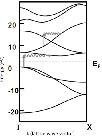
k (lattice wave vector)
Figure 1.5: Indirect transitions in a phonon-assisted photon absorption scheme in a crystalline solid. Two types are represented (intraband and interband). figure from [67].
Now if the electron energy reaches sufficiently large levels it is commonly pro-posed that another ionization mechanism may be activated: the impact ionization. This consists of a CB electron with energy above a threshold energy being able to collide with electron from the VB and thus promote the latter in the bottom of the CB. This may be an iterative process and hence raise the total excitation density exponentially (Nf(t) = Ni∗ 2t/τi, with τi, time between a collisional event,
1.2. EXCITATION PROCESSES IN DIELECTRIC SOLIDS 37 E Ev Ec Eg~ 5-10eV e e
Intraband
heating
e e h h hElectronic
avalanche
Impact
ionization
eFigure 1.6: Illustration of electron ”heating” by inverse bremsstrahlung, eventually followed by impact ionization and resulting in electronic avalanche, in a crystalline solid.
is often qualified as avalanche ionization and it is a very efficient way of electron multiplication and energy relaxation. An illustration of this mechanism (heating plus impact ionization and avalanche) is given in figure 1.6. Coming back to the threshold energy for impact ionization, according to Ridley [80] and for bands with parabolic dispersion:
38 CHAPTER 1. THEORY Eimp = (
1 + 2µ
1 + µ ) ˜Eg (1.9) with µ = mc
mv being the ratio of conduction and relevant valence band effective
masses.
Typically this value is greater or equal to 13.5 eV for SiO2. In order to reach
this kinetic energy, an electron irradiated by 800nm(1.55 eV) photons has to un-dergo 9 inverse Bremsstrahlung absorption events before impact ionization can occur. This for a 60 fs pulse represents a 0.15 fs−1
collision rate with phonons or ions. Such transition rates are not accessible at intensity regimes of the order of 1012 W/cm2: a calculation with an indirect transition rate cross section4 σ at
10−19
cm2 [2] gives rates of only 0.4 × 10⁻³
fs−1
. This result suggests that the intensity has to be raised at surprisingly high values to be able to heat the elec-trons at such values. Impossibility of reproducing photoemission spectra obtained experimentally in CsI motivated Belsky et al. [5] to replace the indirect transitions by direct ones considering that the conduction band is not a simple parabola but moreover it is a certain amount of branches one above the other allowing direct absorption of photons. In CsI the direct transition cross section was found to be 10−16
− 10−17
cm2 (the probability for 1, 2 or 3-photon transitions being the same
at 1013 W/cm2) thus giving rates at 0.2 fs−1
> 0.15 fs−1
. In fact these rates are also dependent on the electron kinetic energy and the wavelength. Presumably a high excitation density may also affect the electron-phonon scattering and thus the indirect transition rate by electrical screening.
All these calculations suggest that at the time scale of the laser pulse dura-tion, no energy relaxation mechanism is activated although the energy absorption mechanisms will most probably dominate the energy relaxation. However, in wide bandgap insulators where the coupling of electrons with phonons is high it is pos-sible that this scattering time becomes of same order of magnitude as the photon absorption time and thus compete with each other preventing impact ionization. Moreover, contrarily to the energy relaxation without energy deposition on the lattice with impact ionization, phonon scattering is actually part of the thermal-ization of the lattice and thus a very efficient mechanism of depositing energy to the medium. Such energy relaxation mechanisms will be discussed in the following section.
4