Université de Montréal
Dynarnical properties of donor-bound excitons
in
Cadmium Telluride
par Wei Li
Département de physique Faculté des arts et des sciences
Mémoire présenté à
la
Faculté des études supérieures en vue de l’obtention du grade de Maîtrise ès science (M.Sc)en Physique
March, 2005
C.
C
L
E
Direction des biblïothèques
AVIS
L’auteur a autorisé l’Université de Montréal à reproduire et diffuser, en totalité ou en partie, par quelque moyen que ce soit et sur quelque support que ce soit, et exclusivement à des fins non lucratives d’enseignement et de recherche, des copies de ce mémoire ou de cette thèse.
L’auteur et les coauteurs le cas échéant conservent la propriété du droit d’auteur et des droits moraux qui protègent ce document. Ni la thèse ou le mémoire, ni des extraits substantiels de ce document, ne doivent être imprimés ou autrement reproduits sans l’autorisation de l’auteur.
Afin de se conformer à la Loi canadienne sur la protection des renseignements personnels, quelques formulaires secondaires, coordonnées ou signatures intégrées au texte ont pu être enlevés de ce document. Bien que cela ait pu affecter la pagination, il n’y a aucun contenu manquant.
NOTICE
The author of this thesis or dissertation has granted a nonexclusive license allowing Université de Montréal to reproduce and publish the document, in part or in whole, and in any format, solely for noncommercial educational and research purposes.
The author and co-authors if applicable retain copyright ownership and moral rights in this document. Neither the whole thesis or dissertation, flot substantïal extracts from it, may be printed or otherwise reproduced without the author’s permission.
In compliance with the Canadian Privacy Act some supporting forms, contact information or signatures may have been removed from the document. While this may affect the document page count, it does flot represent any loss of content from the document.
Université de Montréal faculté des étudies supérieures
Ce mémoire intitulé
Dynamical properties of donor-bound excitons in Cadmium Telluride
Présenté par: Wei Li
À
été évalué par un jury composé des personnes suivantes: Richard Leonelli, Directeur de rechercheNormand Mousseau, Président-rapporteur Carlos $ilva, Membre du jury
To my parents for forever support from far away To my husband for love and support
ACKNOWLEDGMENT$
I would like to express my heartfelt thanks and profound gratitude to my supervisor Prof. Richard Leonelli, flot only for giving me the opportunity to work with his group but for introducing me to a new research field. I deeply appreciate that he gave me plenty of his time and educated me on various aspects of lab and experimental operations. With his kind guidance, support and encouragement, I was able to complete and weil understand this work.
I also especially thank Ms. Zakia Yaïche, Mr. Collin-nadeau Brosseau, Mr. Ghaouti Bentoumi and Mr. Ah Lanacer, who gave a great help to me.
My special thanks are due to Prof. L. A. Hamel who offered us experimental samples.
I would like to thank ail the members ofGCM ofphysics department at University of Montreal.
On a personal note, I wouid like to thank my husband Po Dong for his support and encouragement.
SOMMAIRE
Nous étudions les propriétés dynamiques des excitons liés à des donneurs dans du tellurure de cadmium de grande pureté légèrement dopé avec des donneurs pour compenser les accepteurs. En premier lieu, nous avons réalisé une étude des profils d’émission des excitons liés au donneurs dans le CdTe. L’émission du niveau n=1 de l’exciton lié est bien reproduit par un profil de f ano, tandis que l’émission des niveau n=2, 3 correspond à un profil de Lorentz. Par la suite, nous avons effectué des mesures de photoluminescence en fonction de la température dans la plage spectrale excitonique du CdTe. Ces mesures révèlent la présence de deux mécanismes de transfert d’énergie pour les donneurs peu profonds. Jusqu’à une température d’environ 15 K, le transfert des polaritons excitoniques de la branche inférieure transverse vers la branche excitonique longitudinale domine l’évolution de la population des excitons liés.
À
plus haute température, la libération directe des électrons et des trous contrôle les processus de transfert.Mots clés
Photoluminescence, tellurure de cadmium (CdTe), profil de Fano, excitons liés, polariton
ABSTRACT
We study the dynamical properties of donor-bound excitons in high-purity cadmium telluride with low donor doping to compensate acceptors. Firstly, we performed a study of the emission lineshapes of donor-bound excitons of CdTe as a function of temperature. The emission from the n=1 donor-bound exciton matches pure and simple Fano lineshape, and the emission from n=2, 3 donor bound excitons are well approximated by Lorentzian lineshapes. In addition, temperature-dependent photoluminescence measurements carried in the excitonic region of CdTe revealed the dynamical behavior of two energy transfer paths for shaÏlow donor-bound excitons. When increasing the temperature to about 15K, the energy-transfer channel from the lower polariton-branch excitons to longitudinal excitons results in a descrease of the population of excitons bound to donors. This indicates that the drop of the integrated photoluminescence intensities is due to this exciton-transfer channel. When the temperature is further increased to 24.0 K, the liberation of free electrons and holes from donors controls the transfer process.
Key words:
Photoluminescence, cadmium telluride (CdTe), Fano lineshape, bound exciton, p01 ariton
CONTENTS
ACKNOWLEDGMENT V SOMMAIRE vI ABSTRACT VII CONTENTS VIII LIST 0F TABLES xiLIST 0F FIGURES XII
LIST 0F SYMBOLS xv
CHAPTER 1:
INTRODUCTION 1
1.1 Research motivation 1
1.2 Bound exciton in semiconductors 5
1.3 About this mémoire 10
THEORY
.12
2.1 Polariton . 12
2.2 Lorentzian equation and fano lineshape equation 18
2.3 Activation energy 25
CHAPTER 3:
EXPERIMENTAL DETAILS
29
3.1 Experimental samples 29 3.2 Experimental setup 30CHAPTER 4:
EXPERIMENTAL RESULTS
34 4.1 Low-resolutionPL 344.2
PL
andPLE
spectra 37CHAPTER
5:TEMPERATURE-DEPENDENT PL STUDIES
42CHAPTER 6:
CONCLUSION
51APPENDIX I .60
LIST 0F TABLE
Table I PL energies ofbound-exciton recombinations in CdTe [24-25]. PLenergies of bound-exciton recombinations are listed at the second column. E” is the binding energy for exciton bound to donor or bound to acceptor. ED and EA are ionization energies of donor and acceptor, respectively.
Table II Comparison of equivalent physical parameters of InP, GaAs, and CdTe [14, 29, 36]. m* and
,n11, respectively, are the electron and heavy-hole masses, and 8
and ç, are, respectively, the low and high dielectric constants [37]. E is the n = 1
transverse exciton energy and E is the binding energy of ftee exciton . Eg is hand
gap. ELT is the longitudinal-transverse exciton spiitting energy at k =
o.
15Table III Parameters extracted from the analysis of integrated PL intensities of CdTe. I*(o) is the integrated PL intensity near O K, C1 and C2 are constants relative to E11 and E1, thermal activation energies. 46
Table IV Parameters extracted from the experiment. Luminescence energies E0 of (D0,X),1 , energy E0 +E,2 , the bound energies Eb of (D°,x),1 and
activation energies E,1 and E,2 from the fit parameters in CdTe samples are
LI$T 0F FIGURES
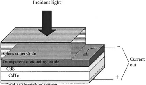
Figure 1.1 A typital Cd$/CdTe solar celi structure (flot to scale). The CdTe/CdS solar celi is based upon the heterojunction formed between n-type CdS and p-type CdTe. Glass substrate protects the active layers and offers the window layer. Transparent conducting oxide acts as the front contact and the window layer to the device. CdS layer provides one haif of the p-fi junction and the window layer. CdTe layer is the active region of the solar ceil and the active junction is formed at the interface between n-type Cd$ layer and p-type CdTe layer. Gold or aluminium is the back contact [10].
Figure 1.2 4.2-K photoluminescence (open circles) of n-type hP [27]. The solid curves are Lorentzian fits to the PL data. a (f,x),1, is the n = 1 free-exciton
transition; b, c, d, and e are, respectively, the n =4, 3, 2, and 1 neutral shallow donor
bound-exciton transitions (D°,x),, ; j=(D0,i) is the neutral shallow donor to free
hole recombination; g = (D,x) is ionized donor bound-exciton transition; h =
(iï°,x) is the neutral acceptor bound-exciton transition; j = (i,x) is the neutral
deep-donor bound-exciton recombination; =
(r°,A°) is the shallow donor-acceptor pair recombination.
Figure 2.1 Dispersion relation for excitonic polarions in CdTe, calculated with the polariton parameters given in Table I. The curve labelled I and II are usually referred to as the “upper” and “lower” branches of the polariton. (b) The polariton group velocity (vg, bottom scale) on the lower branch as a function of polariton energy (left
Figure 2.2 Energy scheme of a Fano interference system: A discrete state d> and continuum e> are coupled by an interaction V. The transition from a common ground state g) to the discrete and continuous states leads to the typical lineshape. 19
Figure 2.3 Natural une shapes for different values of q [3$-39]. Reverse the scale of
abscissas for positive q 21
Figure 2.4 Schematic diagram of activation energy 25 Figure 3.1 Schematic diagram of setup for PL and PLE (flot drawn to scale and
positions represented are approximate). 33
Figure 4.1 Low-temperature FTIR PL data for five samples at the same experimental conditions. The spectral features in inset labeled 1 and 2 are associated with(A0
x)
and
(D0,x)
emission unes, respectively. 35Figure 4.2 The FTIR PL spectrum for CdTe LAH sample at $ K. The sharp features associated with (A0,x) and (D0,x) emission unes are clearly seen
around 1.589eV and 1.593eV, respectively. The other labels are explained in the text.
36
figure 4.3 temperature-dependent Photoluminescence spectra DBE of sample CdTe at T = 1.8 K. The spectrometer was centred at 7787
Â
for DBE spectra. a,b, and e, respectively, represent donor-bound-exciton transitions (D°,X),,=123
with Fano lineshape fits. 40
Figure 4.4 Photoluminescence (PL) and Photoluminescence excitation (PLE) spectra ofCdTe sample recorded at 7.82 K for a detection of (D0,X),, peaks labelled
a, b and c. FE is free exciton peak. The dashed une and solid une are, respectively,
PLandPLE. 41
Figure 5.1 Temperature-dependent PL spectra of CdTe measured at several different temperatures, as indicated on the graph. The peaks labelled by a, b, and, c,
respectively, are n = 1-3 components of donor-bound-exciton transitions (D0,x),1.
The dashed curves are Fano lineshape fits to the relevant transitions.
Figure 5.2 Temperature dependence of the PL intensities of structures a, b, and, c of Figure 8 in a ln(I) plot. Circles, square and diamonds are experimental points. The solid unes are the theoretical fits with two different dissociation energies derived from Eq. (29).
Figure 5.3 Schematic diagram of the dispersion cures of a ‘bare’ exciton (dashed curves) and an exciton-polariton (solid curves) in CdTe. The u-tum arrows indicate the transfer process of converting the excitons xLPB in PLB into the longitudinal
LI$T 0F SYMBOLS
/.J Polarizability of exciton
c Speed of light in vaccum
C1 ith constant linked to the degeneracy of E11 E Reduced energy
E1 Transition energy
EA, ED Ionization energies of donor and acceptor impurities E”, EBX Binding energy of free exciton to the attractive center
Eg Energy gap
EL Longitudinal exciton energy ET Transverse exciton energy
ET(k) Transverse exciton energy at wave vector k ELT, zL TLongitudinal-transverse exciton splitting energy
E11, ET?, ith activation energy and thermal activation energy
E Binding energy of free exciton E0 Energy position
E(D °
,x)
+
,x)’
E(A
°,x)
Spectral positions of(D°,x), (D,x)
andE, s,,, s Reduced energy, low and high dielectric constant
1*
(D° x),i=]2,3 Jntegrated PL intensities of transitions (De,
x),1
1(E) Jntensity at the energy E I. Intensity ofthe ith peak
1*
(o)
ftitegrated PL intensity near O KkT Thermal energy at absolute temperature T k Wave vector
m Static mass ofelectron, electron mass and heavy-hole mass
q Fano lineshape parameter u Width ofthe spectral feature R0 Rydberg for the hydrogen atom f Width ofthe spectral feature (f WHM)
(A0,
x)
Neutral-acceptor-bound exciton(A,x) Ionized-acceptor-bound exciton (D°,
x)
Neutral-donor-bound exciton tD,X) Iionized-donor-bound exciton(D°,
x),1123
n=1-3 components ofthe neutral-donor-bound exciton transitionsD°, x),,
INTRODUCTION
1.1
Research motivation
In recent years, much study interest lias focused on compound semiconductors InP, GaAs and CdTe. They have been widely used for the fabrication of optoelectronic devices such as GaAs/A1GaAs quantum well infrared photodetectors (QWIPs), InGaAs photodetector, CdS/CdTe solar ccli, CdTe/CdZnTe based y -Ray detectors, HgCdTe infrared detector with a CdTe buffer layer and so on, due to their excellent electronic and optical properties [1-4].
The binary compound CdTe is an important direct-band-gap II-VI semiconductor material. The hand gap of CdTe is approximately 1.60 eV at low temperature, higher than those of InP and GaAs (see Table I about equivalent physical parameters of InP, GaAs and CdTe). In the past, the studies of II-VI semiconductor materials was mainiy concentrated on compounds with higlier hand gaps such as ZnSe, ZnTe, ZnS, and CdS, but these semiconductor materiais stili have some fundamental difficulties in applications, since so far they cannot be well produced in both n-type and p-type forms with Ïow resistivity [5]. However, CdTe is the only in II-VI compound semiconductors that can be
prepared in n-type, p-type, or with low resistivity [6-7]. The increasing interest in thc study of CdTe is mainly in its demonstrated applications including t8]:
-solar celis (see the typical CdS/CdTe ceils structure shown in Figure 1), -7-ray detector (CdTe/CdZnTe ‘y-ray detector),
-electro-optic modulators, -nonlinear optical devices,
-room-temperature x-ray detectors,
-optical elements for infrared application.
For several years the polycrystalline thin-film CdTe/CdS solar ceil has been considered to be a promising alternative to the more widely used silicon devices [9]. It has several properties that make it especially attractive:
i. The cost of CdTe solar ceils from polycrystalline materials and glass is potentially much cheaper than buÏk silicon.
ii. The bandgap of CdTe is ideal for solar ceil application because it matches the sunlight spectrum very well.
iii. Thin-films can be prepared using a variety of different techniques due to the chemical and physical properties of the semiconductors.
iv. The absorption coefficient of CdTe is very high so that approximately 99% of the incident light can be absorbed by a layer thickness of only 1tm
(compared with around lOjim for Si), which decreases the quantity of semiconductor required in the applications.
Incident light
Cuent
/
outFigure 1.1, A typital CdS/CdTe solar ceil structure (flot to scale). The CdTe/CdS solar ceil is based UOfl the heterojunction formed between
n-type CdS and p-type CdTe. Glass substrate protects the active layers and offers the window layer. Transparent conducting oxide acts as the front contact and the window layer to the device. Cd$ layer provides one halfof the p-n junction and the window layer. CdTe layer is the active region of the solar ccli and the active junction is formed at the interface between n-type CdS layer and p-type CdTe layer. Gold or aluminium is the back contact [10].
Furthermore, CdTe/CdZnTe (CZT) based y -Ray detectors have been developed intensively and have recently seen significant improvements [11]. These detectors are mainly used in the nuclear industry and nuclear medicine. CZT detectors have high resistivity because of the wide bandgap and also have high photon absorption efficiencies because of the large atomic number Z and high density. In addition, CZT detectors show low noise at room temperature due to thcir high resistivity.
To obtain high-quaïity photoelectric devices with high efficiency, the semiconductor materials must have high purity. Thus, a more detailed physical understanding of the effect of defects and impurities upon device applications seems to be essentiaÏ for further progress
t
12]. For example, R. Benzaquen has reported a temperature dependence of shalïow-donor bound-exciton-emission linewidths and exciton-impurities interactions in high-purity InP in detail [13-14], and E. S. Koteles has extensively investigated high-purity GaAs [15]. For these reasons considerable effort has been spent in growing pure and defect-free high quality CdTe crystals. Numerous studies on CdTe have also been made on crystal growth and photoluminescence (PL) properties with respect to various shallow acceptor- and donor-impurity complexes in the past few decades and many papers have focused on the PL spectra of CdTe, most being directed toward identifying impurities and defects responsible for the various spectral features [16-20]. Therefore it is also important to investigate the basic dynamical properties ofbound exciton in high-purity CdTe as a function of sample growth and application parameters.1.2 Bound excitons in semiconductors
Since rnost semiconductor materials contain significant amounts of impurities and/or defects which can trap excitons, the identification of the bound exciton states provides an important characterization of impurities, which control the electro-optic properties of semiconductors.
In high purity and high quality semiconductors at low temperature, the Coulomb attraction between electrons and holes causes their motion to be correlated and resuits in electron-hole pairs, known as excitons. Similar to the way that free carriers can be bound to (point-) defects, when the sample contains a small number of donors or acceptors (or defects), the excitons can also be bound to these impurities (or defects) via van der Waals interactions [21]. These are known as bound excitons (3E): neutral-acceptor-bound exciton (commonly abbreviated as (A0,X)), ionized-acceptor-bound exciton (to be abbreviated as
(A-,x)
),
neutral-donor-bound exciton (abbreviated as (D°, x))
and ionized-donor-bound exciton (abbreviated as (D X)).Bound excitons give risc to photoluminescence emission at lower energy than that of free excitons. The binding energy E’ of an exciton to the complex is defined as the energetic distance from the lowest free exciton state at kO to the energy of the bound state ofthe exciton.
The spectral positions of the principal excitonic unes usually can be estimated from the following expressions [24]:
EtDO\) = Eg —(Ex +ED)
U)
=Eg —(ED +ED), (2)
E(Aox) =Eg —(E11 +EA), (3)
E(D °
,x)
+ X)
, and,
E(A
°,x)
, respectively, express the spectralpositions of (D0,x), (i,x) and (A°,x). Eg and E are the band-gap energy
and the binding energy of free exciton. ED and EA are the ionization energies of
donor and acceptorimpurities. is the localization coefficient ofthe free exciton. In silicon, first observed by Haynes, bas a value around 0.1 [21, 22, 46]. However, the neutral donors and neutral acceptors have different behaviors in CdTe. Donor bound excitons (DRE) follow =0.2 and many acceptor-bound excitons follow =0.l [23]. The binding energy of free exciton to complex can also be obtained from the optical spectra containing much more detaiÎed information. The binding energies and emission peaks for several different donor- and acceptor-bound excitons and the ionization energies of several donor and acceptor impurities are listed in Table I.
At low temperature the near-band-edge photoluminescence (and absorption) spectra of serniconductor materials (such as direct gap III-V and II-VI semiconductors) is usually dominated by the narrow bound-exciton emission unes. Higli attention is concentrated on these unes since they are extrernely useful for impurity characterization in these materials. Figure 1 .2
Table I PL energies ofbound-exciton recombinations in CdTe [25-26]. PL energies of bound-exciton recombinations are listed at the second column. E”’ is the binding energy for exciton bound to donor or bound to acceptor. ED and LA are ionization energies of donor and acceptor, respectively.
Donor F Ga Al In Cl I N Li Na Sb P As Ag Cu Au (Du, X) (eV) 1.59314 1.59309 1.59305 1.59302 1.59296 1.59284 1.5927 1.5892 1.58923 1.58916 1.5895 1.58897 1.58970 1.58848 1.58956 1.57606 Eb (meV) 3.36 3.41 3.46 3.48 3.54 3.66 3.8 7.2 7.17 7.24 6.8 7.43 6.70 7.92 6.84 20.34 ED (meV) 13.67 13.88 14.05 14.15 14.48 14.60 —1 5.1 EA (meV) 46 56.0 58.0 58.7 65 68.2 92.0 107.5 146.0 263
Acceptor (A°,X) (eV) Eb (meV)
---shows a typical photoluminescence spectrum of an n-type InP at low temperature. Recombination peaks such as (F,x),,1, (D°,x),, (A0,X) and so on are well identified in figure 1.2.
A paper by R. Benzaquen et al (1995) presented a temperature-dependent PL spectroscopy study of the neutral shallow-donor bound-exciton emission in a high-purity, n-type InP [14]. By a simple formula based on the model of a two-step dissociation mechanism, R. Benzaquen analyzed in detail the temperature dependence of the PL integrated intensities of two components of the shallow-donor bound-exciton transitions ((D0,X),312) and revealed the
presence of two dissociation channels: (1). (D°,X)12
D°+x
(2). (D°,x),,12 D° +e+h.
The dissociation channel (1) resuits in the liberation of a free exciton from a shallow neutral donor with activation energy ET] equal to the binding energy Eb of the donor-bound exciton. The channel (2) describes the liberation of a free electron and a free hole from a shallow neutral donor with activation energy
ET2 = E” +
E. When the temperature is increased from 4.2 K to about $ K, the dissociation chaimel (1) dominates the donor-bound-exciton transitions. When the temperature is further increased to 20 K, channel (2) becomes the dominant dissociation path. These results about the dynamics of donor-bound excitons in high-purity InP inspired us to make an effort to explore the dynamics of donor-bound excitons in high-purity CdTe semiconductor.
10
o
z
6-> 4z
Ez
2-I I 1.408 1.412 1.416 1.420 ENiGY (eV)Figure 1.2 4.2-K photoluminescence (open circles) of n-type InP
[27]. The solid curves are Lorentzian fits to the PL data. ci= (f,
x),,1
is then = 1 free-exciton transition; b, e, d, ande are, respectively, the
n 4, 3, 2, and 1 neutral shallow donor bound-exciton transitions (Do
x)
; j = (D°,h) is the neutral shallow donor to free-holerecombination; g =
(D,x)
is ionized donor bound-excitontransition; h (A0,X) is the neutral acceptor bound-exciton
transition; j = (D,
x)
is the neutral deep-donor bound-exciton recombination;j
= (Do, A°) is the shallow donor-acceptor pairrecombination. e — 4 F Cd’i F-’ z I C.) E3 u o Q
1.3
About this mémoire
This work is concerned with the dynamics of donor-bound excitons in high-purity CdTe at low temperature between 1.8 K and 24 K, by analyzing the temperature dependence of the integrated photoluminescence intensity in detail. From the measurements of Fourier-transformed infrared photoluminescence spectra, photoluminescence emission and photoluminescence excitation spectra, we observe (D0,X),1 transitions, interpret the data with a two-step dissociation model and deduce the details ofthe dissociation processes. At the same time we obtain some physicai parameters about donor-bound excitons in high-purity CdTe. Ail the works was done at laboratory G.C.M. (Group ofThin Films) ofthe Université de Montréal.
This mémoire consists ofthe following chapters. In Chapter 2, we review various basic concepts used in our work. We discuss the poiariton concept and polariton dispersion relation in detail. We present Fano iineshape and Lorentzian equations, and introduce the activation energy associated with a two-step dissociation model to be used in our study.
In Chapter 3 we describe the experimental sampies, experimental setups and measurement methods.
In Chapter 4 we present the optical characterization of some CdTe samples including Fourier-transformed infrared photoluminescence spectra,
photoluminescence and photoluminescence excitation spectra, at the low temp erature.
In chapter 5 we analyze the temperature dependence of integrated PL intensity of high-purity CdTe sample and interpret experimental data in detail.
CHAPTER 2
THEORY
Throughout this chapter, some ofthe important concepts and theories directly relevant to this work will be presented in detail. We first provide a review on exciton-polariton in direct-band-gap semiconductors due to the important relation between polaritons and luminescence spectra at Yow temperature. This review is based on the publications of D. Bimberg [28], R. Benzaquen [13-14] and D.E. Cooper [29]. After this review, we discuss the Lorentzian equation which describes the basic lineshape for a homogenous transition, and the Fano lineshape equation which is suited to fit the asymmetric lineshapes in the PL spectra of CdTe. In addition, a two-step dissociation model, which properly explains the temperature-dependent integrated PL intensity and dynamical properties of DBE in high-purity CdTe samples, is introduced.
2.1
Polariton
Toyozawa [30] pointed out for the first time that the luminescence spectra in semiconductors at low temperature should be interpreted in term of polaritons. Using the dispersion relation of exciton-polariton, R. Benazquen has presented exciton-impurities interactions in high-purity InP [14] and E. S. Koteles has thoroughly investigated high-purity GaAs [15].
In direct-band-gap semiconductors such as InP, GaAs and CdTe, exciton-photon strong interactions resuit in the formation of coupled modes calÏed exciton-polaritons (to be abbreviated as polaritons in the latter part), which determine many optical properties ofthe semiconductors. The polariton dispersion curve for CdTe is shown in Figure 2.1, where the curves labelled I and II are usually referred to as the “upper” and “lower” branches ofthe polariton. The energy of the transverse exciton ET(k) is given
by
(4)
where k is the wave vector and M is the exciton mass. ET is the zero-center transverse exciton energy. As a resuit ofthe coupling of pure exciton and photon states, the upper and lower polariton branches are formed, which can be described by a two-branch model (here we are only considering the dispersion relation ofn 1 state) t14-15, 24, 31]: 8b 2ELTE(k) , (k.EQ) (5)
L
E] E(k)[E(k)E2] (k.E=O) (6) 1/2E,,LT =EFIL —E,,T
=[b
+4fi
—h1E,lT
(7)
1599 -1.598 1 .57 1.596 E 1.595 1. 594 -1.593 1.592 O 1O 21O8 3x10⁸ 4x10⁸ k (mfl)
Figure 2i (a) Dispersion re’ation for excitonic polarions in CdTe, calculated with the polariton parameters given in Table I. The curve Iabeled I and II are usually referred to as the “upper” and “Iower” branches of the polariton. (b) The polariton group velocity (vg, bottom scale) on the lower branch as a function ofpotariton energy (left scale) (from [27]).
(b) I ï (a) I
J
II Bott1efl —- I --t - I L 800 1200 1600 2000 2400 2300 - V9 (m/)Table II Comparison of equivalent physical parameters oflnP, GaAs, and CdTe [14, 29, 36]. in and m, respectively, are the electron and heavy-hole masses, and s,, and s are, respectively, the low and high dielectric constants [37]. ET is the n 1 transverse exciton energy and E is the binding energy of free exciton . Eg is hand gap. ELT is the
longitudinal-transverse exciton spiitting energy at k = 0.
fliP GaAs CdTe
m* (a.u.) 0.082m0 O.O67mo O.096mo
m1 (a.u.) 0.85m0 O.64m0 O.81m0
ET (eV) 1.4185 1.5153 1.5954 Eg (eV) 1.424 (16K) 1.519 (0K) 1.607 (10K) E (meV) 4.82 4.2 10.5 b 12.3$ 12.8 10.4 EDo 9.55 10.86 7.1 ELT(meV) 0.13 0.13 0.65
polariton, longitudinal polariton and longitudinal-transverse exciton spiitting energy. (k,E), c, and E are, respectively, the dielectric function ofthe medium including the polariton contribution, the speed of light in vaccum, and the polariton energy. 3 is the exciton polarizability, and 8b is the background dielectric constant exciuding the polariton contribution. EL is the longitudinal exciton energy. ELT represents the longitudinal-transverse exciton spiitting
energy at k= O which gives a measurement ofthe coupling strength between the
uncoupled longitudinal and transverse excitons at k= O. It is to be noted that only
the transverse excitons can interact with the electromagnetic field.
Polariton effects can be observed experimentally through reflectivity, transmission, and luminescence spectroscopy [32], and with particular success by Raman spectroscopy [33]. The emission of a photon by a polariton is fundamentally different from corresponding processes associated with most excited states, since electromagnetic energy resonant with the polariton band travels through the crystal as a polariton. Thus in order for a polariton in the interior of a crystal to emit as a photon, it must first migrate to the crystal surface, where it can be converted to a photon and thus radiated out from the crystal.
The polariton dispersion curve appropriate for CdTe (n=1) is presented in figure 2.1 (a). Figure 2.1 (b) displays the polariton group velocity on the lower polariton branch as a function of energy, which is related to the derivative of the polariton dispersion curve for the lower polariton branch. On the upper polariton branch (abbreviated as UPB) of the polariton dispersion curve, the polaritons
start out exciton-like at energy EL and quickly become photon-like with increasing wave vector. On the lower polariton branch (LPB), at the large wave vector, the polaritons are predominantly exciton-like, whereas, at small wave vectors they are photon-like below energy ET. The nature of the polariton
dispersion relation has a profound effect on the luminescence mechanism in this energy region [29, 33]. for example, the lower-branch polaritons may be scattered by phonons into the energy region below or near ET where radiative decay of polaritons can take place through their photon components. Furthermore, it lias been shown that polariton-impurity scattering bas a marked effect on the polariton luminescence une shape [34]. As the polariton relaxes toward the “knee” region of dispersion curve (Figure 2.1 (a)), the rate of photon emission decreases, forming a “bottleneck” [15, 35] which aÏlows the polariton population to reach a thermal equilibrium with the crystal temperature, where the lifetimes of polaritons are the longest. As shown in Figure 2.1 (b), the group velocity of the lower-branch polaritons, VLPB = h’dELPB / dk, varies very rapidly
with energy, and has a minimum just above the bottleneck (Figure 2.1 (b)). Velocity-dependent scattering processes are greatly enhanced in this energy region. This enhancement in scattering together with the low group velocity resuits in much siower diffusion of these polaritons. These phonon scattering rates decrease as polaritons beÏow ET become more photon-like, and on the other hand, polaritons are short-lived because they have high group velocity. The existence of a propagating mode such as the polariton in the crystal lias a profound effect upon the
photoluminescence (PL) process, which must be viewed within the framework of a transport problem. Instead of a population of free excitons, which can recombine anywhere in the crystal pro ducing photons that are free to excite the crystal unhindered, there is a population of polaritons that can produce external PL if the excitation first travels to the surface. In the polariton picture, a polariton impinging on the crystal interface has a certain probability of being transmitted and a certain probability of being reftected back.
2.2 Lorentzian and Fano lineshape equations
In this section we mainly introduce two lineshape equations, Lorentzian and Fano lineshape equations. They fit well DBE unes in the PL spectra ofCdTe.
A) Lorentzian function
The Lorentzian function is the singly peaked function given by
1(E) , (8)
)2 U
1(E): intensity at energy E
I.: intensity of ith peak (maximum value at E= Ef)
E: energy position
Ef: center energy of peak (transition energy) u: half width at half maximum (HWHM)
The Lorentzian une shape is symmetric about its central energy E1 of the peak with a HWHM u. Ef ami u wiÏl be treated as free parameters of the fit. The Lorentzian lineshape is a typical lineshape for homogeneously broadening optical transitions..
B) Fano lineshape equation
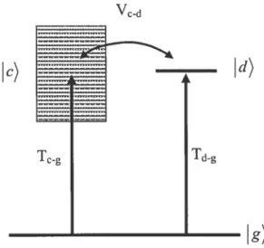
f ano interference is an universal phenomenon in physics which can be observed in various systems such as rare gases spectra, photodissoziation, bulk GaAs in magnetic field, superlattice in electric field, impurity ions in semiconductors, electron-phonon
Vc-d
c) d)
Tc.g Td.g
g)
Figure 2.2 Energy scheme of a Fano interference system: A discrete state d> and continuum
le>
are coupled by an interaction V. The transition from a common ground state g) to the discrete and continuous states leads to the typical lineshape.coupling and many more [3$-42]. In general, this interference arises by an interaction of a discrete state with an energetically degenerate continuum of states. The energy scheme of a Fano interference system is drawn in Figure 2.2. Excitation can take place from ground state g) either into a discrete state d) or into continuum state corresponding to excitation path Tdg afld Tcg. The coupling manifests itself due to quantum mechanical interference Vd between discrete state d) and continuum state
c).
The equation ofFano lineshipe is given by [43- 44]:
(q+e)2
(9) (1+ 2)
q: lineshape parameter
s: the reduced energy given by: 2(E-E
)
(10) F
E: energy position Ef: transition energy
f: the width ofthe spectral feature (FWHM)
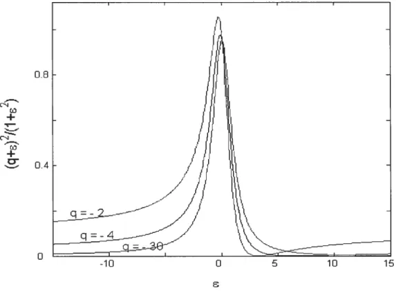
Figure 2.3 shows Fano lineshapes for different values of q. The Fano lineshape equation shows an asymmetric line shape at the energy E of the peak with a FWHM I. q, Ef and F will be treated as free parameters ofthe fit. The sign of q
0.8 c-l o + r ri o ± o o 10 o 5 10 15
Figure 2.3 Natural une shapes for different values of q [43-44). Reverse the scale of abscissas for positive q.
22
determines the asymmetry of the une due to interference effects. It is positive when the interaction is repulsive and negative when the electron-hole interaction is attractive. When
I
is much greater than 1, Eq. (9) becomes equivalent to Eq. (8) in the region where the signal is the strongest.We show a brief derivation for the simpïest case of one discrete resonance and one continuum (the derivation follows S. Glutsch’s “Exciton in Low-Dimensional Semiconductors”) [45]. first, we start the derivation with Hamiltonian matrix element
Hand transition matrix elernent M).
E0V1 V2• M0
Vj*Ej O... M1
H= ,, M)= . (11)
V O E2•• M2
Where E0 and E1 (1> 0 in the latter part of this section) are the energy of the discrete state and the energy of continuum. V,, M0 and M1 are, respectively, the coupling matrix element between the discrete state and the continuum, the transition matrix element to the discrete and transition matrix element to the continuum. The J’Ç, and M1 can be expressed as — v(E1) . M — u(E1) 12 - D(E1)’
-where D(E1)=1 /(E,1 —E1) is the density of states.
2
I. (13)
t EA—w+te)
R(z)rr (H—z)’; H1) =EAl);
(1 t’)
=
;‘)K1
=
1.Where is te normalized eigenvectors of H , and e= +0 is a positive
infinitesimal. ai is the resonance frequency. The function R(z) is the resolvent and its
matrix elements are the Green’s function. With mathmeticaÏ relations it follows that
2 —] R00(z)= H0—z—’ V1 i Es—z R10(z)
=
R01,,(z)=
— R00(z),, ; in >0 (14) E1—z E,,,—z R1 (z)=
61m + VR00 (z)V, ; i, rn >o
E1 —z (E1 —zXE,,,
—z)Then the optical susceptibiÏity is equal to:
MV
J
t
VMJ
M()=
M0—Z’ I I Ro0(ai+ieMo—Z’ “ “HZ’
t E, —kW+l E)]
L
in E,,, —L,ai+l E)] / E1 —w+t eFor D(E1)—> cc, the following summation can be replaced be intergration on the right:
Z’
=dE v2(E)=fdE v(%t(E) (15)
i E1—(a+ie) E—(o+i)
=JdE p2(E) =K+1iA
t E1—(w+ie) E—(cû+i) 2
where F, G, K, T A, and zl are real numbers with
f=2jcv2, zI=2rvp;A=22rp2andz12=fA. (16)
With the above equations, the optical susceptibility becomes
(M _G_1z1)22
+K+1A. (17)
E0—F—(o+i)—if 2
The imaginary part ofthe optical susceptibility is the absorption coefficient a with
a(a)= Ini(o);
a(o)=Irn(cc)=A=r,u2, (18)
To avoid having a sum of a discrete resonance and a continuous background and obtain analytic function near real axis, assume that nontrivial case f> O. Then let areplace w+i e in eq. (17). We use the relation
()
to eliminatc the parameter fino.
After some algebrausing eq. (16), (17) and (18), the absorption equals toa(o)Im(w)[E0-F-o-(M0-G)H/A]2 19 a() — a
()
— (E0 —F — )2 + A / A2 Letco-E0-F - M0 -G q-z1 (20) f f \2 aa)) q+6) a(JD) 1+62
At last, get the famous Fano formula:
(21)
2.3 Activation energy
2
t
Activation energy3
Reaction path
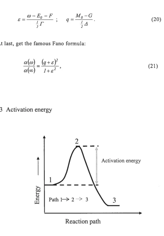
Figure 2.4 Schernatic diagram of activation energy. Reaction pathis1— 2 —3.
Activation energy is defined as the energy that must be invested in a reaction to get
activation energy. If the reaction with the original state 1 and the end state 3 can happen, it must pass a medial sate 2.
R. Benzanquen analyzed the integrated PL intensities of DBE unes in high-purity
InP using the following equation:
1* T — J*(O)
(D°,X),,1,
H—
Nt
J+ Clexp[—(El/kBT)]
I(DOX): the temperature dependence ofthe integrated PL intensities
I*(O): the integrated PL intensity near O K
E: the ith activation energy
C.: the ith constant linked to the degeneracy of E1
This activation energy E1 can often be related to the energy that is necessary to ftee an electron from a bound state.
To get equation (22), firstly, there are the following assumptions [13, 28]:
(1) The exciton complex has at least three states: ground-state energy E0, where it is bound, and two higher states with energies E1 and E2, where they are dissociated. The two paths of dissociation have energies ET] =E1 —E0 and
(2) Consider each electron-hole pair as a complete system and the rest of the crystal including ail the other electron-hole pairs merely as a temperature bath. At the same time the pair-pair correlations are neglected.
(3) The three-level system is in thermal equilibrium at temperature T.
According to these assumptions the electron-hole pairs among the three levels are governed by the Boltzmann distribution. Then there are the following equations: NQ(T)+NJ(T)+N2(T)=NG(T), (23) N‘ (E1-E0) =--‘-e kT , (24) N0(T) a0 ‘r (E,—E0) “2’ kT , (25) N0(T)
where, N0(T), N1(T), and N2(T) are the average numbers of bound excitons being in the levels E0, E1, and E, at the temperature T, respectively; a0, a1, and a2 are the degeneracies ofthese levels. NG(T) expresses the total number
of electron-hole pairs within the three levels at the temperature T.
Equations (23), (24) and (25) are combined to form another formula for NG(T)
f
(E1—E0) (E1—E0)kT kT
, (26)
Here NG(T) is regarded as constant at the experimental temperature. Then we
have NG (T) NG
(o)
= N0(o).
This assumption is consistent with the experimentsas seen from the good fit oftheory and experiment [22, 34]. Therefore from Eq. (26) we obtain:
N (T) E,1 E,,
N0
(o)
= [i +C1e kT +C7e kT , (27)
where c1 = a1 / a0, C2 = a2 /a0, E11 = E1 —E0, E,2 =E2 —E0.
If we don’t consider any change in the radiative recombination probability with temperature, then NO(T)/NG(T) can be exactly applied to the radiative
recombination process with energy ha. From Eq. (27) we get
E,,
= ]+C1e kF +C2e kF (2$)
where the physical meaning ofthis equation is the ratio ofthe radiative intensity
‘T at temperature T and the radiative intensity I at O K when two activation
processes are considered.
When N activation processes are taken into account, Eq. (28) is expressed as
= N . (29)
CHAPTER 3
EXPERIMENTAL TECHNIQUE
3.1 Experimental samples
The various transition processes in semiconductors strongly depend on the temperature, the concentration of impurities, the intensity and waveÏength of exciting light. In our case, a variety of cadmium telluride samples from various sources with different dopant were examined, and the CdTe sample with the greatest amount of donor-bound-exciton emissions was selected for our study. These samples include CdTe LAH, CdTe/Sb, CdTe/As, CdTe #1, and CdTe #1$. CdTe LAH sample is a commercial sample doped with a little donor to compensate acceptors. CdTe/Sb sample contains about 130-ppm ofSb byweigh. CdTe/As sample is a CdTe sample doped with As of unknown concentration. CdTe # 1 and CdTe #18 are nominally pure CdTe samples. CdTe LAH sample was provided by Professor L. A. Hamel and the other CdTe samples were grown at laboratory of Université de Liège (Belgium).
Before the samples were mounted in the cryostat cooled by liquid helium to take the photoluminescence measurements, it was necessary to clean them in order to eliminate the impurities on the surface. For this purpose, the samples were
soaked in a 2% Br/CH3OH solution for approximately five minutes, and then rinsed with a methanol solution [29].
3.2 Experimental setup
Photoluminescence (PL) is an important and the most common physical phenomena widely used to characterize semiconductors, which depicts a sample’s energy structure while possibly revealing other important material features [47]. In brief, photons (commonly from a laser source), with energy Etaser greater than the bandgap Eg ofthe semiconductor sample studied, are directed onto the surface ofthe sample, and they are partially reflected, absorbed, and transmitted by the sample. The absorbed photons create electron-hole pairs by exciting electrons to the conduction hand or to the energy states within the gap in the sample. Meanwhile, electrons can lose part of their energy and transfer from the conduction hand to lower energy levels. PL occurs when photons, which are produced as a resuit ofvarious recombinations events ofelectrons and holes, are emitted from the sample surface or the bulk. The emitted photon has a specific energy EPL corresponding to the material’s specific structure, composition and
quality. The intensity and spectral content of the photoluminescence is also a direct measure of various important material properties.
PL spectroscopy is usually performed at low temperatures in order to obtain spectral resolution ofdifferent emission lines. Nevertheless, PL spectroscopy at room temperature has also received increasing interest, because room-temperature PL mapping ofband-edge emission and deeper defect-related
emissions has proved to be a useful technique to characterize the homogeneity and crystalline quality of II-VI semiconductor materials.
Photoluminescence excitation (PLE) spectroscopy is another popular technique for studying thin epilayers grown on opaque bulk substrates, and it has been proved that PLE spectroscopy is very powerful to investigate excited states of bound-exciton complexes [48]. In brief PLE is a technique that records the ernission intensity ofa particular photon energy from the samples as a function of the excitation photon energy. PLE spectra usually exhibit sorne resonance peaks, which indicate that the ernission can be particularly strong excited at certain photon energies.
In the measurements of PL and PLE spectra of CdTe sample, the samples were mounted in the cryostat cooled by liquid helium at approximately 5K. To obtain steady-state PL spectra, the optical excitation cornes frorn a tunable Ti:sapphire laser purnped by an laser with an output power rnaintained at 150 mW. The excitation light is focused on the sample by a convergent lens, and at the same tirne the PL collected by a set of lenses is dispersed by a 1-m double spectrorneter with holographie gratings and then detected by a CCD camera cooled with liquid nitrogen, or by a GaAs photomultiplier cooled by the Peltier effect. For PL measurements, the spectrometer was centred at 7787
À
for DBE spectra, and for PLE, the laser was controlled by a feedback systern adjusting the laser intensity in order to get constant intensity of the Ti-sapphire laser in the used wavelength range. During the experirnent, additional measurements between 1.8 and 4.5 K were taken by immersing the sample in superfluid liquid heliurn (T < transform temperature 2.2 K). An attenuator withtransmission coefficient equal to 0.2% is inserted in order to reduce the laser power. The diagram of the experimental setup is shown in figure 3.1.
Figure 3.1 Schematic diagram of setup for PL and PLE (not drawn to scale and positions represented are approximate).
1. Argon laser 2. Ti-sapphire laser
3. Detector for stabilization of power with retroaction ofthe laser 4. Convergent lens 5. Cryostat 6. Sample 7. Sets oflenses 8. double spectrometer 9. Photomultiplicatorr GaAs/Carnera CCD 10. photon counter
11. Computer (control and acquisition)
6 7
•LD
11
CHAPTER 4
OPTICAL CHARACTERIZATION 0F CdTe SAMPLES
4.1
Low-resolution PL spectra
Prior to the high spectral resolution photoluminescence measurements, we took the measurements of low-resolution photoluminescence spectra of all samples in order to obtain the spectra more quickly. Low-resolution-photoluminescence (to be abbreviated as LRPL) measurements were performed with the samples in a He flow cryostat at the temperature of 5-8 K and using a BOMEM DA$ Fourier transform infrared spectrometer (abbreviated as FTIR). FTIR spectra can show the emission features in a large range of energy and allow the identifications of the emission unes.
Figure 4.1 and 4.2 display the FTIR photoluminescence spectra for all CdTe samples and single CdTe LAH sample, respectively, and the spectra were recorded at the same experimental conditions using a Si detector. It is observed that the CdTe LAH sample shows the sharpest (D°,x) emission unes in figure 4.1 (see the inset of figure 4.1). Furthermore, the spectra ofCdTe LAH, CdTe/As and CdTe/Sb samples also show very clearly the (A°,x) emission unes. In the FTIR photoluminescence spectrum for single CdTe LAH sample (sec figure 4.2), the sharp features associated with the emission lines of
C -D (sJ fM C Q) 4-J C C
o
a
o
in -DEnergy (eV)
Figure 4.1 Low-temperature FTIR PL data for five samples at the same experimental conditions. The spectral features in inset labeled 1 and 2 are associated with (A0
x)
and (Dox)
emission lines, respectively.(n 4-’ (n G) 4-’
o
4-,‘:2-o
(n-o
Figure 4.2 The FTIR PL spectrum for CdTe LAH sample at 8 K. The sharp features associated witl
(A°,x)
and (D0,X) emission unesare clearly seen around 1.589eV and 1.593eV, respectively. The other labels are explained in the text.
1.3 1.35 1.4 1.45 1.5 1.55 1.6
(A°,x) and (DO X) are clearly seen around 1.589 eV and 1.593 eV, respectively. The spectral feature labelled I, which appears -21 meV below the
(A°,X) emission unes, is associated with the photon replica ((A°,X)-LO); the feature labelled II is donor-acceptor pairs (to be abbreviated as DAP or (D0, A0));
and the spectral features labelled III near 1.4 eV band are associated with the native defect complexes which are very important for the applications of CdTe semiconductors. In figure 4.1 we can note that the emissionlines of native defect complexes are also present in the FTIR PL spectrum of CdTe #1 sample and that the spectra of CdTe/As, CdTe/Sb, CdTe #18 samples hardly show this feature. (A0X)-LO and (D0,A0) lines can also be strongly, or weakly seen in the
spectrum of other samples.
As seen in the previous part ofthis section the five samples have different FTIR PL features at the low temperature and CdTe LAH sample shows not only the emission lines of (D0,X) but other important features such as (A0,X)LO, DAP
and native defect complexes. Our goal was to find a CdTe sample with highest purity. We especially rely on the emission unes of (D0,X) which are much
sharper in CdTe LAH sample than the other ones. We thus selected this sample to proceed to the study ofthe dynamics of (D0,X).
We took the PL spectrum ofthe CdTe sample at 1.8K with the condition that the spectrometer was centred at 7787
À
in order to obtain clear and exact (D°,x),1_123 peaks. Figure 4.2 displays the(D°,x),123
transitions in the region between 1.592-1.595 eV at 1.8K. (D°,x),1123 transitions have Fano lineshape fits (see APPENDIX II about the fitting parameters).Virtual excitation or transition in spectrum means the creation of a state with the same wave function as the excited state, but with an energy which is different from the eigenenergy of this excited state. Any transition which has a finite lifetime has an energy which can be written according to the uncertainty principle of quantum mechanics as
AExAth. (30)
Where, zlE is the lifetime broadening, i.e., the spectral energy of full width at half maximum. At is the radiative recombination lifetime of the donor bound exciton. h is the ratio ofPlank constant h to 2w.
The radiative recombination lifetime ofthe free exciton is in the nanosecond range [29]. In the spectrum of Figure 4.3, the values of the lifetime broadening for (Do X) 123 states are, respectively, 0.11meV, 0.16meV, and 0.10meV, which approximately correspond to the radiative recombination lifetimes of the donor-bound excitons on the order of picosecond (6.Ops, 4.lps, and 6.6ps) according to uncertainly principle of equation (30). The radiative recombination lifetime of the donor-bound exciton in CdTe is thus shorter than that of the free
exciton. This is in agreement with homogeneous broadening of the donor-bound exciton.
In addition, PLE measurement of CdTe sample was taken in order to know well the spectral features at energies ofinterest to our studies. Figure 4.4 shows a PLE spectrum of CdTe sample monitoring the emission at 1.5904eV at 7.8 K. For comparison, the PL spectrum is shown along with the PLE spectrum at the same temperature. In the PLE spectrum at energies ofinterest in our study, we are able to identify the three strongly excited spectral features labelled a, b and c, which are associatedwiththe (D0,x),123 peaks inthePL spectrum. The featurepeaks exhibited in the PLE spectrum are near 1.5927eV, 1.5932eV, and 1.5938eV. The PLE spectrum is surprising since the presence of (D0,X),1123 features is flot expected in the excitation spectrum of ABE (acceptor-bound excitons). It has been mentioned that the (D0,X),1 lifetime broadening is around 6 ps. This might indicate that the binding lifetime of excitons to donors is so short that the excitons are hable to get free from the donors. The most possible reason for the present of (D°,x),7123 peaks in the PLE spectrum ofABE is that free andbound excitons are constantly converted each in the other.
In order to further examine this hypothesis, the next chapter is focussed on studying the temperature dependence ofthe PL in details.
U) C :3 I C5 > U) C G) I. C
Figure 4.3 Temperature-dependent Photoluminescence sp ectra DBE of sample CdTe at T = 1.8 K. The spectrometer was centred
at 7787
À
for DBE spectra. The dashed curves corresponding with a, b, and c, respectively, represent donor-bound-exciton transitions (D°,X),1=123 with F ano lineshape fits.1.5911 1.5917 1.5923 1.5929 1.5936 1.5942
figure 4.4, Photoluminescence (PL) and Photoluminescence excitation (PLE) spectra of CdTe sample recorded at 7.8 K for a detection of
(D°,x),,
peaks labelled a, b and c. FE is free exciton peak. The dashed une and solid une are, respectively, PL and PLE.U) C .ri I >-I— U) z w I z -J o-U) I C z .0 L >-I ci) z w H z w -J o-1592 1594 1596 1598 1.6 1 602 1804 ENERGY (eV)
CHAPTER 5
TEMPERATURE-DEPENDENT PL STUDIES
The temperature-dependent PL spectra of CdTe LAH sample were measured as a function of increasing temperature from 1.8 to 24.0K (keeping ail other parameters constant). Figure 5.1 shows the temperature-dependent PL spectra of the CdTe sampie observed at five different temperatures (respectively, 4.4K,
8.8K, 14.3K, 22.6K and 24.0K).
Three nice, clearly resolved
(D°,x),123
transitions at 1.5927eV, 1,5933eV,andl.5938eV can be observed at low temperature. The intensity ofthe DBE une decreases with increasing temperatures and becomes very weak at 24 K. The une shapes of (D0,X)11_123 transitions are asymmetric, with the low-energy side broader than the high-energy side. These asymmetric peaks can be well fitted with Fano lineshapes using equation (9) (see APPENDIX II about ail parameters ofFano fits).
In fact, whiie modeling the transitions, we experienced a great difficulty to fit the asymmetric (D0,X),1 transitions in the low energy region with the low-energy side broader than the high-energy side. To get an ideal fitting curve, we have tested severai asymmetric distribution functions such as Gumbel, Genlogistic,
(n L >1 1-; G) G) Q C G) Q
(n
G) CE
o
4-,o
QEnergy (eV)
Figure 5.1 Temperature-dependent PL spectra of CdTe measured at several different temperatures, as indicated on the graph. The peaks labelled by a, b, and, c, respectively, are n = 1-3 components ofdonor
bound-exciton transitions . The dashed curves are F ano
1.591 1.5916 1.5922 1,592e 1.5934 1.5941
fisk, Weibull and Lsqdlrtz lineshapes. In no case the asymmetric peaks agreed with these tested asymmetric functions. At last, the Fano lineshape function was found to be the closest to our ideal model. It is very interesting that the fitted curve ofDBE asymmetric transitions agree well with f ano lineshape (sec peak a in figure 4.3) although it is flot exactly Fano interference [38-39]. Finally, attention may be paid to interpreting the sign of the parameter q, which is certainly negative because the peak in figure 5.1 sharply siopes on the high-energy shoulder. At the same time the value ofsmall
II
(between about 3-9) for the (D°,x),11 (i.e., peak a at 1.5927eV) displays the transition of pure and simple Fano lineshape, and then the very largeII
(between about 25-170) ofthe (Do X)23 (i.e., peak b at 1.5933eV and peak c at 1.5938eV) indicates approximate Lorentzian lineshapes with homogeneous energy broadening written as Eq. (8).In analyzing the temperature-dependent integrated PL intensity, we use equation (11) to fit the data for 1*(D°,x),1123. When N= 1, using this equation
to fit the value of C. and E1 fails to reproduce the data at the experimental temperatures. We got approximate good fits using this equation with N 2 except that the experimental points don’t agree very well with the fitting points in the region of 4-5 K, probably due to laser fluctuations. Figure 5.2 shows the temperature dependence ofthe integrated PL intensities 1*(D° X)123 versus
U) I— z D Q::: >-H U) z w I— z 12 10 8 6 4
Figure 5.2 Temperature dependence of the PL intensities of structures a, b, and, e of Figure 8 in a ln(I) plot. Circles, square and diamonds are experimental points. The solid unes are the theoretical fits with two different dissociation energies derived from Eq. (29).
0.1 0.2 0.3 0.4 0.5 l/T (K1)
Table III. Parameters extracted from the analysis of integrated PL intensities of CdTe.
i*(o)
is the integrated PL intensity near O K,C1 and C2 are constants relative to E,1 and E,, activation energi es.
Table IV Parameters extracted from the experiment. Luminescence energies E0 of (D0,X),, energy E0 +E,2, the bound energies Eb f
(Do X) and activation energies E,1 and E,2 from the fit
parameters in CdTe samples are given in table.
CdTe peak a peak b peak c
J*(O) (iO) 202.9(±105.4) 918.1(+O.02) 150.8(+O.Ol) C1 132.8(+57.O) 542.3(+43.2) 525.9(±56.1)
C2 (1&). 622.9(±O.3) 1722.9(+O.02) 213.3(±O.O1)
E,1 (meV) O.68(+O.06) O.39(±O.02) O.51(+ 0.02)
E,, (meV) 1 5.7(±1 .5) 15.9(±O.9) 1 0.7(±O.7)
CdTe E0 Ex+Eb E,1 E,2
S ample (eV) (eV) (meV) (meV) (meV)
n=1 1.5927 14.2 3.7 O.68(±O.06) 15.7(+l.5)
n=2 1.5933 13.6 3.1 0.39(+0.02) 15.9(+0.9)
from CdTe sample of Figure 5.1, at the temperatures between 1.8 K and 24.0 K (see Table VI ofAPPENDIX III about 1*(D°,x),j23 at different temperature). All
parameters extracted from fitting I*(D0,x),J,3 are shown in Table III. The solid
line in Figure 5.2 is the best-fit to the data (circles, squares and diamonds) giving two activation energies E11 and E12, with E11 and E17 corresponding to the values of the slope at the regions of low and high temperature, respectively. Thus at low-temperature region (about 1.8-15K) the activation process is dominated by the dissociation process (or other energy-transfer path) with the lower activation energy E11. At about 15K the dissociation process with another activation energy E12 begins to dominate in DBE system. We eliminate the possibility of energy-transfer path that the lower-state (D°,
x)
is converted into the higher-state(D°,x)
(i.e., (D°,x),,1(r°,x),17
or (D°,x),72 —>(D°,x),13
)
since I(DOX) decrease ail together as the temperature is increased to 24 K.
The dissociation of the (D°,
x)
system can obey four different general processes according to the dissociation of (A°,X) system [28]. Thus we can compare the measured energies E11 with the dissociation energy ETabCd corresponding to each of these processes. The four general processes are written as:(a) Dissociation resulting in a free exciton
(DoX)Do+X Ea =E(D°,X)=E,.
(D0,X)D0 +e+h, ETb
=Eo +E.
(c) Dissociation resulting in one free electron:
(D°,X)(D,X)+e, ETC = Eo +E E(D°,h) ETb E(D°,h) <ETb
(d) Dissociation resulting in two free electrons and one free hole: (D°,X)D+e+e+h,ETd=ETb+ED»ETb.
In CdTe, we know that ALT = 065meV, E =10.5meV, Eg =1.6069eV [37].
First, we consider the dissociation process (a) shown above. This process predicts an activation energy E,1 = It is obvious that the dissociation process ta)
cannot cause the drop of I*(D0,x),J]23 associated with energy E,1 since E,1 is
a very small value compared with ETabCd (see columns 4 and 5 of Table IV), the
process (c)-(d) can’t either. That indicates that there exists another energy-transfer path. E,1 is very close to the longitudinal-transverse energyLT t=O.65meV).
At the lowest temperature, most of the exciton-polaritons reside in the bottleneck region of the LPB. When the temperature is raised, the population of excitons coupled with photons in the LPB tto be abbreviated as XLPB) is decreasing because some is converted into the longitudinal excitons (abbreviated as XL). The population of excitons in LPB directly affect the population of exciton trapped to impurities. We explain I*(D0,x),1123 decreasing with increasing
temperature as the shortage of exciton source in the LPB due to the energy-transfer channel XLPB —* XL . figure 5.3 displays the schematic
TJPB
Longitudinal Ex citon f
• exciton
figure 5.3 Schematic diagram of the dispersion cures of a ‘bare’ exciton (dashed curves) and an exciton-polariton (solid curves) in CdTe. The u-tum arrows indicate the transfer process of converting the excitons XLPB in PLB into the longitudinal
E11 in CdTe.
The dissociation process (b) predicts the activation energy ETb = +E
given in column 3 of Table IV. Comparison between column 3 and column 6 indicates that ETb and E12 are very close. Thus we deduce that the dissociation procession (b) resulting in the liberation of a free electron and hole from a donor is another energy-transfer path associated with energy E12.
In summary, as mentioned in the introduction, a simple formula based on the model of a two-step dissociation mechanism can be used to interpret the donor-bound-exciton transitions in high-purity InP studied by R. Benzaquen [14]. Here, we show that the behavior of the donor-bound-exciton transitions can also be described very well by the same formula in high-purity CdTe. At high-temperature region the dynamical properties of donor-bound exciton in high-purity CdTe agree with those in InP and the process (b) is responsible for donor-bound-exciton dissociation in CdTe. But flot as expected, the dissociation path at low-temperature region is completely different. The energy-transfer path is XLPB —> XL rather than the process (a) as in InP for the
DBE dissociation at low temperature in CdTe. The dissociation path (a) does not happen when the temperature is increased from low to high region since figure 5.2 does not exhibit the slope corresponding to the third activation energy of about 3 meV.
CHAPTER 6
CONCLUSION
In this work, the dynamical properties of donor-bound excitons in a high-purity CdTe sample that is slightly doped with low donor to compensate for the acceptors, were studied using Fourier transform infrared and photoluminescence spectroscopic measurements.
We studied the optical characterization on a set of different CdTe samples. The FTIR PL spectrum of each sample shows one or several spectral features associated with (A°,r), (Do, r), (A0, x)-Lo, donor-acceptor pair and the native defect complexes. The CdTe LAH sample with verywell (D°,r) feature was the better one selected for our following study.
PL data were taken from 1.8 K to 24.0 K. PL spectra ofhigh-purity CdTe display clearly the presence of emission peaks of donor-bound excitons at 1.5927 eV, 1.5933 eV, and 1.593$ eV, and furthermore, show asymmetric donor-bound-exciton transition peaks with the low-energy side broader than the high-energy side in low-energy region. In fact, while modeling the asymmetric transitions to gain an ideal fits, we have tried to use several asymmetric distribution functions including Gumbel, Genlogistic, Fisk, Weibull and Lsqdlrtz lineshapes. The asymmetric peaks failed to agree with these tested asymmetric functions. At last, the Fano lineshape
function was found to be the closest to our ideal mode!. Fano interference is a typical feature of the optical spectrum of low-dimensional semiconductors. We have introduced Fano interference in detail in the second chapter. The (D°,X),11
transition matches pure and simple Fano lineshape with negative q although it is flot exactly real Fano interference, and
(r°, x),123
have approximate Lorentzian lineshapes which describe the basic lineshapes for a homogenous broadening. According to the uncertainty principle and measurement of PL spectra, the values of thelifetimebroadening are ofthe order of 0.1 meV, which approximately correspond to the radiative recombination lifetimes ofthe donor-bound exciton, around 6 ps.km order to verify the spectral features of CdTe sample, we study the excitations with PLE measurements at energies of interest to our studies. Three strong spectral features which are associated with (D°,x),7173 recombinations are observed in the PLE spectrum of acceptor-bound excitons. This might indicate that the short-lived lifetimes of (D0,X),1 resuit in exciton escape from the binding of donors. The most possible reason for the presence of (D°,X),7123 peaks in the PLE spectrum of acceptor-bound excitons is that free and bound excitons are constantly converted each in the other.
We analyzed the temperature dependence of integrated intensities of the n =1, 2 and 3 components ofthe donor bound-exciton transitions in high-purity CdTe in detail by using a simple formula. This formula is based on the model of a two-step dissociation mechanism. We showed that, the behaviors of the
donor-bound-exciton transitions are welldescribed approximately by this formula. A rernarkable feature of this model is that it includes two energy-transfer channels usually corresponding to two activation energies. When the temperature increases to about 15K, we got a very small activation energy which is iower than those of ail the dissociation processes expected. And this energy is associated with the dispersion relation of exciton-poiariton. At the iowest temperature, most of the exciton-polaritons occupy the positions of the bottleneck region of the lower-polariton-branch. Some of the excitons in the lower-polariton-branch state are converted into the longitudinal excitons with temperature increasing so that the population of excitons bound to donors becornes srnali. This energy-transfer channel from iower-polariton-branch excitons to longitudinal excitons resuits in the lower activation energy, i.e., the first drop of PL integrated intensity 1*(D° x),1123 of CdTe sample.
Exciton-polariton dispersion thus piay a very important role in the opticai properties of semiconductors at low temperature. When the temperature is further increased to 24.0 K, the second actvation energy with a bigger value appears within this temperature range. As expected, this activation energy agrees with the dissociation process controlled by the liberation of free electrons and holes from donors. Cornpared with the resuits in high-purity InP studied by Robert Benzaquen [14], the dissociation channel with the liberation of a free electron and a free hoie from a shallow neutral donor does flot happen as expected at the low-temperature region in CdTe. But at the higli-temperature region the dynamical behavior of donor-bound excitons becomes very weil identicai.
To summarize, our resuits clearly demonstrated that shallow donor-bound excitons in high-purity CdTe have the dynamical behavior oftwo energy-transfer paths in the 1.8-24.0 K range by the measurements oftemperature-dependent photoluminescence. One path is lower-polariton-branch excitons transfer to longitudinal excitons and another one is liberation of free electrons and holes from donors. Undoubtedly, it would be very meaningful in the future to study the dynamical properties of acceptor-bound excitons and other exciton complexes. furthermore, it remains to understand why the emission unes of donor-bound excitons are so well described by a Fano profile since this cannot be explained by the interference between a discrete state and a continuum.
REFERENCE $
[1] Razeghi M and Duchemin J P 19841 Ciyst. Growth 70 145
[2] NA LI, N1NG LI, W. LU, X.
Q.
LIU et al., Superlattices and Microstrttctures, Vol. 26, No. 5,1999t3] Gallant M, Puetz N, Zemel A and Shepherd F R 1988 Appi. Phys. Lett. 52 733 CdTe::: 1. G.N. Panin, C.Diaz-Guerra and J.Piqueras, Semicond. Sci.
Technol.13, 576, (1998).
[4] MH. Aslan, W. Song, J. lang, D. Mao, and RI. Collins, D. H. Levi and R. K. Ahrenkiel, S. C. Lindstrom and M. B. Johnson, Mat. Res. Soc. Symp. Proc., 485 p.203 (1992).
[5] B. Monemar, E. Molva, and, Le Si Dang, Phys. Rev. 333, 1134—1145 (1986)
t6] F. V. Wald, Rev. Phys. Appt. Vol. 12 #2 (1977), 277
[7] R. O. Beli, Rev. Phs. Appi. Vol. 12 #2 (1977), 391
[8] J. Aguilar-Hernandez, Gerardo Contreras-Puente at al., Jpn. J. Appi. Phys., Vol. 33, p37-41 1994
[9] K. Durose, P.R. Edwards, D.P. Halliday, J. Crystal Growth 197, 733 (1999).
[10] M. Rami, E. Benamar, M. Fahoume, F. Chraibi, and A. Ennaoui, M.J. CONDENSED MATTER Vol. 3, Num. 1,66(2000)
![Table I PL energies ofbound-exciton recombinations in CdTe [25-26]. PL energies of bound-exciton recombinations are listed at the second column](https://thumb-eu.123doks.com/thumbv2/123doknet/7703406.246034/24.918.188.804.314.951/table-energies-ofbound-exciton-recombinations-energies-exciton-recombinations.webp)
![Figure 1.2 4.2-K photoluminescence (open circles) of n-type InP [27]. The solid curves are Lorentzian fits to the PL data](https://thumb-eu.123doks.com/thumbv2/123doknet/7703406.246034/26.918.249.734.103.681/figure-photoluminescence-open-circles-type-solid-curves-lorentzian.webp)

![Table II Comparison of equivalent physical parameters oflnP, GaAs, and CdTe [14, 29, 36]](https://thumb-eu.123doks.com/thumbv2/123doknet/7703406.246034/32.918.258.742.462.897/table-comparison-equivalent-physical-parameters-oflnp-gaas-cdte.webp)