HAL Id: hal-01292186
https://hal-univ-rennes1.archives-ouvertes.fr/hal-01292186
Submitted on 22 Mar 2016
HAL is a multi-disciplinary open access archive for the deposit and dissemination of sci-entific research documents, whether they are pub-lished or not. The documents may come from teaching and research institutions in France or abroad, or from public or private research centers.
L’archive ouverte pluridisciplinaire HAL, est destinée au dépôt et à la diffusion de documents scientifiques de niveau recherche, publiés ou non, émanant des établissements d’enseignement et de recherche français ou étrangers, des laboratoires publics ou privés.
Copyright
Dielectric properties of hybrid perovskites and
drift-diffusion modeling of perovskite cells
Laurent Pedesseau, Mikael Kepenekian, Daniel Sapori, Yong Huang, Alain
Rolland, Alexandre Beck, C. Cornet, Olivier Durand, Shijian Wang, Claudine
Katan, et al.
To cite this version:
Laurent Pedesseau, Mikael Kepenekian, Daniel Sapori, Yong Huang, Alain Rolland, et al.. Dielectric properties of hybrid perovskites and drift-diffusion modeling of perovskite cells. SPIE Proceedings Se-ries, 2016, Physics, Simulation, and Photonic Engineering of Photovoltaic Devices V, 9743, pp.97430N. �10.1117/12.2214007�. �hal-01292186�
Dielectric properties of hybrid perovskites and drift-diffusion
modeling of perovskite cells
L. Pedesseau*a, M. Kepenekianb, D. Saporia, Y. Huanga, A. Rollanda, A. Becka, C. Corneta, O. Duranda, S. Wanga, C. Katanb, J. Evena
aUniversité Européenne de Bretagne, INSA, FOTON UMR 6082, 35708 Rennes, France; bInstitut des Sciences Chimiques de Rennes, UMR 6226, CNRS – Université de Rennes 1, France
ABSTRACT
A method based on DFT is used to obtained dielectric profiles. The high frequency ε∞(z) and the static εs(z) dielectric
profiles are compared for 3D, 2D-3D and 2D Hybrid Organic Perovskites (HOP). A dielectric confinement is observed for the 2D materials between the high dielectric constant of the inorganic part and the low dielectric constant of the organic part. The effect of the ionic contribution on the dielectric constant is also shown. The quantum and dielectric confinements of 3D HOP nanoplatelets are then reported. Finally, a numerical simulation based on the SILVACO code of a HOP based solar cell is proposed for various permittivity of MAPbI3.
Keywords: Dielectric confinement, Quantum confinement, Nanoplatelets, hybrid Perovskites
1. INTRODUCTION
3D Hybrid Organic Perovskites (HOP) of general formula RMX3 with R is an organic cation, M is a metal and X a
halide have recently attracted a lot of attention in the photovoltaic community due to the fast increase of their efficiency from 3.8 % in 20091 to 19.3 % in 20142. Actually, the hybrid organic perovskites can be in the 3D or also in the 2D structure. Since the 90s, they are investigated for applications such as Field Effect Transistor (FET)3 and Light-Emitting Diode (LED)4. The size of the organic cation R impact directly on the shape of the HOP: for small R (such as CH
3NH3+),
the 3D structure is preferred whereas for large R (such as C4H12N+) the HOP exhibit a 2D structure with alternating
organic and inorganic layers. The structure determines the electronic and optical properties of the HOP such as the excitonic properties. Indeed 2D HOP present an exciton with a large binding energy5 due to a dielectric confinement6,7
whereas 3D HOP exhibit an exciton screened by the polar rotation of the organic cations8–10. We propose here a method
to describe dielectric profiles that goes beyond the standard approximation for dielectric constant profiles with abrupt interfaces11,12. Besides, nanostructures of HOP have been recently reported13–20. Quantum size effects of nanoplatelets of CH3NH3PbI3 are also treated. With the benefit of the all solution process21–23 of HOP and mature silicon technology24,25,
a cost-effectively and high-efficiency perovskite/Si tandem26–30 is desirable. The HOP top cell is studied for three
different permittivity. The device simulation is based on the SILVACO31 code dedicated to optoelectronic device design.
*laurent.pedesseau@insa-rennes.fr
Citation: L. Pedesseau ; M. Kepenekian ; D. Sapori ; Y. Huang ; A. Rolland, A. Beck ; C. Cornet ; O. Durand ; S. Wang ; C. Katan ; J. Even, " Dielectric properties of hybrid perovskites and drift-diffusion modeling of perovskite cells ", Proc. SPIE 9743, Physics, Simulation, and Photonic Engineering of Photovoltaic Devices V, 97430N (March 14, 2016); doi:10.1117/12.2214007;http://dx.doi.org/10.1117/12.2214007
2. INFINITE AND STATIC DIELECTRIC CONSTANT OF 3D AND LAYERED HYBRID PERVOSKITE
The dielectric constant is obtained from the response of the material to an external electric field. Dielectric profiles are computed from an ab initio method based on Density Functional Theory (DFT)11,32. An external field is applied to a slab
along its stacking axis (z) inducing a variation of the electron density. The electron density is then averaged in the directions perpendicular to the stacking axis and a nanoscopic average is performed in the direction (z). The induced polarization pind(z) is obtained by partial integration of the induced electron density. Finally the dielectric profile is
obtained with ) ( ) ( 0 0 z p E E z ind ext ext − = ε ε ε .
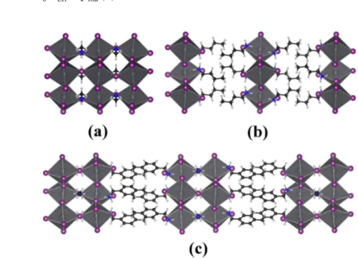
Figure 1. Figure of the 3D HOP CH3NH3PbI3 (a), the 2D HOP (C4H12N)2PbI4 (b) and 2D/3D HOP (C10H24N)2PbI3
CH3NH3PbI4 (c).
The dielectric constant depends of the frequency of the applied electric field and is described by a tensor for anisotropic system. For optical frequencies, the high frequencies dielectric constant ε∞(z) is related to the reaction of the electronic
density to the electrical field. For lower frequencies, the contribution of the ionic charges are added to the static dielectric constant εs(z). Here we propose the dielectric profiles ε∞(z) and εs(z) of HOP with different shape. The systems
considered are the 3D HOP CH3NH3PbI3, the 2D HOP (C4H12N)2PbI4 and the 2D/3D (C10H24N)2PbI3CH3NH3PbI4
(Figure 1). The slabs are constructed from the bulk materials: the 3D slab is built from the (010) pnma phase of CH3NH3PbI3 with 6 octahedra PbI3, the 2D/3D slab is composed of 2 two-octahedra inorganic layers sandwiched by
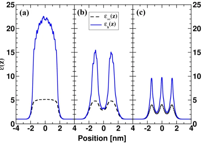
aromatic organic cations and the 2D slab is composed of 3 one-octahedron inorganic layers sandwiched by aliphatic organic cations. The profiles ε∞(z) and εs(z) are depicted in the Figure 2. Considering first the high frequency dielectric
profile of MAPbI3 (Fig2.a), the bulk dielectric constant is recovered in the center of the slab with a value about 5.6. It is
in good agreement with the measured value of 6.533. Adding the ionic contribution the dielectric constant obtained is
four times higher reaching the value of 22.0 at the center of the slab. This value is closed to the experimental value that oscillates between 23.3 and 37 depending of the sample, the phase and the method34–36. In the case of the 2D HOP, the dielectric constant exhibits a dielectric confinement between the low dielectric constant of the organic part and the high dielectric constant of the inorganic part (Fig 2.c). The 2.1 value obtained for the organic part compares well with experimental values reported around 2.2-2.337. The dielectric constant of the inorganic part amounts 4.0 and is as
expected lower than the one obtained for the bulk due to dielectric confinement. For lower frequencies, disagreeing to the 3D HOP, the static dielectric constant of the inorganic part is only 2.5 times larger. It can be explained by the anisotropy of the system with an organic layer that softens the ionic displacement response of the inorganic part. Finally the dielectric profiles of the 2D/3D are depicted in fig 2.b. The high frequency dielectric constant reaches 4.8 and stands
between the 2D and the 3D HOP value. Adding the ionic contribution, the value increases to 15 this is 3 times larger than the infinite one. The enhancement is larger than for the 2D because the system is less anisotropic. We can also note that the ionic contribution is not critical for the organic dielectric constant.
Figure 2. High frequency dielectric profiles ε∞(z) and static dielectric profiles εs(z) for the 3D HOP CH3NH3PbI3 (a), the
2D/3D HOP (C10H24N)2PbI3CH3NH3PbI4 (b) and the 2D HOP (C4H12N)2PbI4 (c).
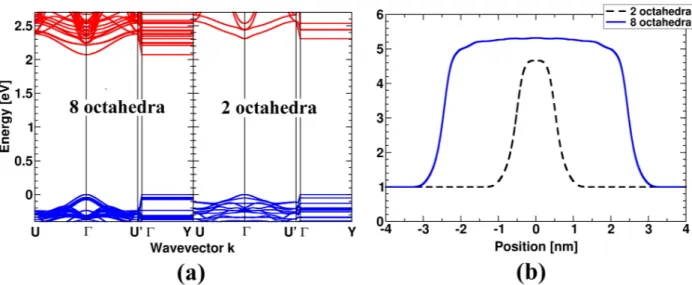
3. DIELECTRIC AND QUANTUM CONFINEMENTS IN NANOPLATELETS OF MAPBI3 In this section, we investigate the quantum and dielectric confinement in nanoplatelets of CH3NH3PbI3. Two slabs of 2
and 8 octahedra are constructed from the pnma phase of CH3NH3PbI3. The surface perpendicular to the stacking axis of
the slabs corresponds to the (010) direction of the bulk material. The bands structures are shown in the figure 3.a. The two nanoplatelets exhibit a direct band gap at the Γ point such as for the bulk material. The energy band gap obtained for 2 octahedra slab is about 2.48 eV and is higher than the thicker one which is amounts 2.07 eV. Figure 3.b. shows the dielectric profiles ε∞(z) obtained for the two slabs. The dielectric confinement is due to the reduction of the slab thickness
has shown on Fig. 3b from 8 to 2 octahedra. Nanoplatelets of CH3NH3PbI3 were recently reported20 and an increase of
the band gap with decreasing the thickness was observed. However the band gap did not increase as anticipated by various model. It might be explained by an increase of the exciton binding energy which compensates the band gap increase and which is retrieved in our calculations.
Citation: L. Pedesseau ; M. Kepenekian ; D. Sapori ; Y. Huang ; A. Rolland, A. Beck ; C. Cornet ; O. Durand ; S. Wang ; C. Katan ; J. Even, " Dielectric properties of hybrid perovskites and drift-diffusion modeling of perovskite cells ", Proc. SPIE 9743, Physics, Simulation, and Photonic Engineering of Photovoltaic Devices V, 97430N (March 14, 2016); doi:10.1117/12.2214007;http://dx.doi.org/10.1117/12.2214007
Figure 3. Band structures (a) and high frequency dielectric profiles ε∞(z) (b) for the slabs of MAPbI3 considered.
4. DIELECTRIC VARIATION ON PEROVSKITE TOP CELL
Silvaco Atlas device simulator is used to numerically solve Poisson’s equation coupled with the continuity equations for both electrons and holes under steady state conditions. Figure 4.a shows the energy band diagrams of MAPbI3 based
solar cell under an equilibrium state. The Fermi levels (Ef) of each layer are aligned through electron current flowing,
while the vacuum levels are shifted according to affinities plus the differences of the conduction bands and Ef, or the
work-function of electrodes. On the top of FTO cathode (Fig. 4.a), the structure successively consists of 141nm TiO2,
350nm MAPbI3 and 36nm HTM ended with Au anode. The basic parameters of each layer are shown in Table 1, with
several permittivity of MAPbI3 according to experimental measurements37,38,39 and simulations41. The TiO2, MAPbI3
and HTM are assumed to be intrinsic with unintentionally doping level equals to 1e1942, 1e1543,44 and 3e1845. The profile
of the refractive image index of MAPbI3 derived from the UV-vis diffuse reflectance spectroscopy46.
Table 1: Electronic properties of the multilayers in the MAPbI3 based solar cell cited from literatures. The carrier life
time of MAPbI3 are calculated according to the diffusion length and mobility.
TiO2 MAPbI3 HTM
Permittivity /
8547 6.538,39,47,
31.938, 7041 3.5347 Doping level cm3 ND=1e1942 NA=1e1544,48 NA=3e1845 Affinity eV 4.149,50 3.9 2.0545 Eg, 300K eV 3.551,52 1.4845 2.9845 Mobility cm2V-1s-1 0.252853 6.254,55 0.00147 Carrier life time µs 0.000656,57 0.1 0.1
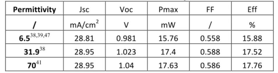
Figure 4 b and Table 2 present the photovoltaic results achieved from MAPbI3 based solar cell under 1 sun illumination
(AM1.5), with three different permittivity of MAPbI3. By increasing the permittivity of MAPbI3, the VOC is improved
more than 6% from 0.981V for the lower permittivity to 1.04 for the higher permittivity. In comparison, the effect on the Jsc is almost negligible from 28.81 to 28.95.
Figure 4. (Color online) Energy band diagrams of MAPbI3 based solar cell under an equilibrium state. The conduction band,
valence band and vacuum level are depicted in blue, greed and orange respectively, with red dash dot line indicating the Fermi level. The device structure is presented above the vacuum level. (a). The current density versus the Voltage, for different permittivity of MAPbI3. (b).
The simplified equivalent circuit model58 for a Photovoltaic Cell reveals that the shunt resistance is not affected too
much but the series resistance is decreasing. When the series resistance is decreasing and the shunt resistance is identical, the fill factor is also increasing as one reported on Table 2. As a consequence, the performance of solar cell is improved more than 10%. This value relates well with the experimentally measured efficiency of 17% (CH3NH3PbI3)43,
well support our simulation for the further investigations of HOP tandem cells.
Table 2: Photovoltaic results of the MAPbI3 solar cell studied.
Permittivity Jsc Voc Pmax FF Eff
/ mA/cm2 V mW / %
6.538,39,47 28.81 0.981 15.76 0.558 15.88
31.938 28.95 1.023 17.4 0.588 17.52 7041 28.95 1.04 17.63 0.586 17.76
5. CONCLUSION
In this paper, dielectric profiles of 3D, 2D-3D and 2D Hybrid Organic Perovskites (HOP) are proposed using a method based on DFT calculations. The frequency-dependence of dielectric constant is treated by comparing high frequency ε∞(z) and the static εs(z) dielectric profiles. A dielectric confinement is found for the layered HOP due to the contrast of
the dielectric constant between the organic and the inorganic layers. The quantum and dielectric confinements of 3D HOP nanoplatelets are also investigated. A device simulation of HOP based solar cell is performed. This simulation indicates some key parameters which are important for the optimization of HOP cells performances. An initial optimized HOP based with 17% efficiency is obtained in agreement with experimental measurements.
Citation: L. Pedesseau ; M. Kepenekian ; D. Sapori ; Y. Huang ; A. Rolland, A. Beck ; C. Cornet ; O. Durand ; S. Wang ; C. Katan ; J. Even, " Dielectric properties of hybrid perovskites and drift-diffusion modeling of perovskite cells ", Proc. SPIE 9743, Physics, Simulation, and Photonic Engineering of Photovoltaic Devices V, 97430N (March 14, 2016); doi:10.1117/12.2214007;http://dx.doi.org/10.1117/12.2214007
REFERENCES
[1] Kojima, A., Teshima, K., Shirai, Y.., Miyasaka, T., “Organometal Halide Perovskites as Visible-Light Sensitizers for Photovoltaic Cells,” J. Am. Chem. Soc. 131(17), 6050–6051 (2009).
[2] Zhou, H., Chen, Q., Li, G., Luo, S., Song, T. -b., Duan, H.-S., Hong, Z., You, J., Liu, Y., et al., “Interface engineering of highly efficient perovskite solar cells,” Science 345(6196), 542– 546 (2014).
[3] Kagan, C. R., “Organic-Inorganic Hybrid Materials as Semiconducting Channels in Thin-Film Field-Effect Transistors,” Science 286(5441), 945–947 (1999).
[4] Chondroudis, K.., Mitzi, D. B., “Electroluminescence from an Organic−Inorganic Perovskite Incorporating a Quaterthiophene Dye within Lead Halide Perovskite Layers,” Chem. Mater.
11(11), 3028–3030 (1999).
[5] Tanaka, K., Takahashi, T., Kondo, T., Umebayashi, T., Asai, K.., Ema, K., “Image charge effect on two-dimensional excitons in an inorganic-organic quantum-well crystal,” Phys. Rev. B 71(4) (2005).
[6] Pedesseau, L., Jancu, J.-M., Rolland, A., Deleporte, E., Katan, C.., Even, J., “Electronic properties of 2D and 3D hybrid organic/inorganic perovskites for optoelectronic and photovoltaic applications,” Opt. Quantum Electron. 46(10), 1225–1232 (2014).
[7] Even, J., Pedesseau, L., Dupertuis, M.-A., Jancu, J.-M.., Katan, C., “Electronic model for self-assembled hybrid organic/perovskite semiconductors: Reverse band edge electronic states ordering and spin-orbit coupling,” Phys. Rev. B 86(20) (2012).
[8] Even, J., Pedesseau, L.., Katan, C., “Analysis of Multivalley and Multibandgap Absorption and Enhancement of Free Carriers Related to Exciton Screening in Hybrid Perovskites,” J. Phys. Chem. C 118(22), 11566–11572 (2014).
[9] Miyata, A., Mitioglu, A., Plochocka, P., Portugall, O., Wang, J. T.-W., Stranks, S. D., Snaith, H. J.., Nicholas, R. J., “Direct measurement of the exciton binding energy and effective masses for charge carriers in organic–inorganic tri-halide perovskites,” Nat. Phys. 11(7), 582– 587 (2015).
[10] Fang, H.-H., Raissa, R., Abdu-Aguye, M., Adjokatse, S., Blake, G. R., Even, J.., Loi, M. A., “Photophysics of Organic-Inorganic Hybrid Lead Iodide Perovskite Single Crystals,” Adv. Funct. Mater. 25(16), 2378–2385 (2015).
[11] Even, J., Pedesseau, L.., Kepenekian, M., “Electronic surface states and dielectric self-energy profiles in colloidal nanoscale platelets of CdSe,” Phys Chem Chem Phys 16(45), 25182– 25190 (2014).
[12] Sapori, D., Kepenekian, M., Pedesseau, L., Katan, C.., Even, J., “Quantum confinement and dielectric profiles of colloidal nanoplatelets of halide inorganic and hybrid organic–inorganic perovskites,” Nanoscale (2015).
[13] Schmidt, L. C., Pertegás, A., González-Carrero, S., Malinkiewicz, O., Agouram, S., Mínguez Espallargas, G., Bolink, H. J., Galian, R. E.., Pérez-Prieto, J., “Nontemplate Synthesis of CH 3 NH 3 PbBr 3 Perovskite Nanoparticles,” J. Am. Chem. Soc. 136(3), 850–853 (2014).
[14] Zhang, F., Zhong, H., Chen, C., Wu, X., Hu, X., Huang, H., Han, J., Zou, B.., Dong, Y., “Brightly Luminescent and Color-Tunable Colloidal CH 3 NH 3 PbX 3 (X = Br, I, Cl)
Quantum Dots: Potential Alternatives for Display Technology,” ACS Nano 9(4), 4533–4542 (2015).
[15] Fu, Y., Meng, F., Rowley, M. B., Thompson, B. J., Shearer, M. J., Ma, D., Hamers, R. J., Wright, J. C.., Jin, S., “Solution Growth of Single Crystal Methylammonium Lead Halide Perovskite Nanostructures for Optoelectronic and Photovoltaic Applications,” J. Am. Chem. Soc. 137(17), 5810–5818 (2015).
[16] Zhu, F., Men, L., Guo, Y., Zhu, Q., Bhattacharjee, U., Goodwin, P. M., Petrich, J. W., Smith, E. A.., Vela, J., “Shape Evolution and Single Particle Luminescence of Organometal Halide Perovskite Nanocrystals,” ACS Nano 9(3), 2948–2959 (2015).
[17] Tyagi, P., Arveson, S. M.., Tisdale, W. A., “Colloidal Organohalide Perovskite Nanoplatelets Exhibiting Quantum Confinement,” J. Phys. Chem. Lett. 6(10), 1911–1916 (2015).
[18] González-Carrero, S., Galian, R. E.., Pérez-Prieto, J., “Organometal Halide Perovskites: Bulk Low-Dimension Materials and Nanoparticles,” Part. Part. Syst. Charact. 32(7), 709–720 (2015).
[19] Gonzalez-Carrero, S., Galian, R. E.., Pérez-Prieto, J., “Maximizing the emissive properties of CH3NH3PbBr3 perovskite nanoparticles,” J Mater Chem A 3(17), 9187–9193 (2015).
[20] Sichert, J. A., Tong, Y., Mutz, N., Vollmer, M., Fischer, S., Milowska, K. Z., García Cortadella, R., Nickel, B., Cardenas-Daw, C., et al., “Quantum Size Effect in Organometal Halide Perovskite Nanoplatelets,” Nano Lett. 15(10), 6521–6527 (2015).
[21] Liang, P.-W., Liao, C.-Y., Chueh, C.-C., Zuo, F., Williams, S. T., Xin, X.-K., Lin, J.., Jen, A. K.-Y., “Additive Enhanced Crystallization of Solution-Processed Perovskite for Highly Efficient Planar-Heterojunction Solar Cells,” Adv. Mater. 26(22), 3748–3754 (2014). [22] Chen, Q., Zhou, H., Hong, Z., Luo, S., Duan, H.-S., Wang, H.-H., Liu, Y., Li, G.., Yang, Y.,
“Planar Heterojunction Perovskite Solar Cells via Vapor-Assisted Solution Process,” J. Am. Chem. Soc. 136(2), 622–625 (2014).
[23] Jeon, N. J., Noh, J. H., Kim, Y. C., Yang, W. S., Ryu, S.., Seok, S. I., “Solvent engineering for high-performance inorganic–organic hybrid perovskite solar cells,” Nat. Mater. 13(9), 897–903 (2014).
[24] Kim, J., Battaglia, C., Charrière, M., Hong, A., Jung, W., Park, H., Ballif, C.., Sadana, D., “9.4% Efficient Amorphous Silicon Solar Cell on High Aspect-Ratio Glass Microcones,” Adv. Mater. 26(24), 4082–4086 (2014).
[25] Masuko, K., Shigematsu, M., Hashiguchi, T., Fujishima, D., Kai, M., Yoshimura, N., Yamaguchi, T., Ichihashi, Y., Mishima, T., et al., “Achievement of More Than 25% Conversion Efficiency With Crystalline Silicon Heterojunction Solar Cell,” IEEE J. Photovolt. 4(6), 1433–1435 (2014).
[26] Filipič, M., Löper, P., Niesen, B., De Wolf, S., Krč, J., Ballif, C.., Topič, M., “CH3NH3PbI3 perovskite/silicon tandem solar cells: characterization based optical simulations,” Opt. Express 23(7), A263 (2015).
[27] Loper, P., Niesen, B., Moon, S.-J., Martin de Nicolas, S., Holovsky, J., Remes, Z., Ledinsky, M., Haug, F.-J., Yum, J.-H., et al., “Organic–Inorganic Halide Perovskites: Perspectives for Silicon-Based Tandem Solar Cells,” IEEE J. Photovolt. 4(6), 1545–1551 (2014).
Citation: L. Pedesseau ; M. Kepenekian ; D. Sapori ; Y. Huang ; A. Rolland, A. Beck ; C. Cornet ; O. Durand ; S. Wang ; C. Katan ; J. Even, " Dielectric properties of hybrid perovskites and drift-diffusion modeling of perovskite cells ", Proc. SPIE 9743, Physics, Simulation, and Photonic Engineering of Photovoltaic Devices V, 97430N (March 14, 2016); doi:10.1117/12.2214007;http://dx.doi.org/10.1117/12.2214007
[28] Mailoa, J. P., Bailie, C. D., Johlin, E. C., Hoke, E. T., Akey, A. J., Nguyen, W. H., McGehee, M. D.., Buonassisi, T., “A 2-terminal perovskite/silicon multijunction solar cell enabled by a silicon tunnel junction,” Appl. Phys. Lett. 106(12), 121105 (2015).
[29] Bailie, C. D.., McGehee, M. D., “High-efficiency tandem perovskite solar cells,” MRS Bull.
40(08), 681–686 (2015).
[30] Bailie, C. D., Christoforo, M. G., Mailoa, J. P., Bowring, A. R., Unger, E. L., Nguyen, W. H., Burschka, J., Pellet, N., Lee, J. Z., et al., “Semi-transparent perovskite solar cells for tandems with silicon and CIGS,” Energy Env. Sci 8(3), 956–963 (2015).
[31] Silvaco Inc., “ATLAS user’s manual,” Sunnyvale, CA (2012).
[32] Daniel, S., Kepenekian, M., pedesseau, laurent., Katan, C.., even, jacky., “Quantum confinement and dielectric profiles of colloidal nanoplatelets of halide inorganic and hybrid organic-inorganic perovskites,” Nanoscale (2015).
[33] Hirasawa, M., Ishihara, T., Goto, T., Uchida, K.., Miura, N., “Magnetoabsorption of the lowest exciton in perovskite-type compound (CH3NH3)PbI3,” Phys. B Condens. Matter 201, 427–430 (1994).
[34] Onoda-Yamamuro, N., Matsuo, T.., Suga, H., “Dielectric study of CH3NH3PbX3 (X = Cl, Br, I),” J. Phys. Chem. Solids 53(7), 935–939 (1992).
[35] Poglitsch, A.., Weber, D., “Dynamic disorder in methylammoniumtrihalogenoplumbates (II) observed by millimeter-wave spectroscopy,” J. Chem. Phys. 87(11), 6373 (1987).
[36] Lin, Q., Armin, A., Nagiri, R. C. R., Burn, P. L.., Meredith, P., “Electro-optics of perovskite solar cells,” Nat. Photonics 9(2), 106–112 (2014).
[37] Solsona, F. J. A.., Fornies-Marquina, J. M., “Dielectric properties of ten primary amines at microwave frequencies as a function of temperature,” J. Phys. Appl. Phys. 15(9), 1783–1793 (1982).
[38] Poglitsch, A.., Weber, D., “Dynamic disorder in methylammoniumtrihalogenoplumbates (II) observed by millimeter-wave spectroscopy,” J. Chem. Phys. 87(11), 6373–6378 (1987). [39] Hirasawa, M., Ishihara, T., Goto, T., Uchida, K.., Miura, N., “Magnetoabsorption of the
lowest exciton in perovskite-type compound (CH3NH3)PbI3,” Phys. B Condens. Matter 201, 427–430 (1994).
[40] Minemoto, T.., Murata, M., “Device modeling of perovskite solar cells based on structural similarity with thin film inorganic semiconductor solar cells,” J. Appl. Phys. 116(5), 054505 (2014).
[41] Lin, Q., Armin, A., Nagiri, R. C. R., Burn, P. L.., Meredith, P., “Electro-optics of perovskite solar cells,” Nat. Photonics 9(2), 106–112 (2014).
[42] Forro, L., Chauvet, O., Emin, D., Zuppiroli, L., Berger, H.., Lévy, F., “High mobility n-type charge carriers in large single crystals of anatase (TiO2),” J. Appl. Phys. 75(1), 633–635 (1994).
[43] Kim, J., Lee, S.-H., Lee, J. H.., Hong, K.-H., “The Role of Intrinsic Defects in
Methylammonium Lead Iodide Perovskite,” J. Phys. Chem. Lett. 5(8), 1312–1317 (2014). [44] Yin, W.-J., Shi, T.., Yan, Y., “Unusual defect physics in CH3NH3PbI3 perovskite solar cell
absorber,” Appl. Phys. Lett. 104(6), 063903 (2014).
[45] Leijtens, T., Ding, I.-K., Giovenzana, T., Bloking, J. T., McGehee, M. D.., Sellinger, A., “Hole Transport Materials with Low Glass Transition Temperatures and High Solubility for Application in Solid-State Dye-Sensitized Solar Cells,” ACS Nano 6(2), 1455–1462 (2012).
[46] Dang, Y., Liu, Y., Sun, Y., Yuan, D., Liu, X., Lu, W., Liu, G., Xia, H.., Tao, X., “Bulk crystal growth of hybrid perovskite material CH3NH3PbI3,” CrystEngComm 17(3), 665–670 (2014). [47] Gagliardi, A., Auf der Maur, M., Gentilini, D., di Fonzo, F., Abrusci, A., Snaith, H. J.,
Divitini, G., Ducati, C.., Di Carlo, A., “The real TiO2/HTM interface of solid-state dye solar cells: role of trapped states from a multiscale modelling perspective,” Nanoscale 7(3), 1136– 1144 (2015).
[48] Buin, A., Pietsch, P., Xu, J., Voznyy, O., Ip, A. H., Comin, R.., Sargent, E. H., “Materials Processing Routes to Trap-Free Halide Perovskites,” Nano Lett. 14(11), 6281–6286 (2014). [49] Aharon, S., Cohen, B. E.., Etgar, L., “Hybrid Lead Halide Iodide and Lead Halide Bromide in
Efficient Hole Conductor Free Perovskite Solar Cell,” J. Phys. Chem. C 118(30), 17160– 17165 (2014).
[50] Dymshits, A., Henning, A., Segev, G., Rosenwaks, Y.., Etgar, L., “The electronic structure of metal oxide/organo metal halide perovskite junctions in perovskite based solar cells,” Sci. Rep. 5, 8704 (2015).
[51] Kim, S. Y., “Simultaneous determination of refractive index, extinction coefficient, and void distribution of titanium dioxide thin film by optical methods,” Appl. Opt. 35(34), 6703 (1996).
[52] Tanemura, S., Miao, L., Jin, P., Kaneko, K., Terai, A.., Nabatova-Gabain, N., “Optical properties of polycrystalline and epitaxial anatase and rutile TiO2 thin films by rf magnetron sputtering,” Appl. Surf. Sci. 212-213, 654–660 (2003).
[53] Gentilini, D., Gagliardi, A., Auf der Maur, M., Vesce, L., D’Ercole, D., Brown, T. M., Reale, A.., Di Carlo, A., “Correlation between Cell Performance and Physical Transport Parameters in Dye Solar Cells,” J. Phys. Chem. C 116(1), 1151–1157 (2012).
[54] Savenije, T. J., Ponseca, C. S., Kunneman, L., Abdellah, M., Zheng, K., Tian, Y., Zhu, Q., Canton, S. E., Scheblykin, I. G., et al., “Thermally Activated Exciton Dissociation and Recombination Control the Carrier Dynamics in Organometal Halide Perovskite,” J. Phys. Chem. Lett. 5(13), 2189–2194 (2014).
[55] Motta, C., El-Mellouhi, F.., Sanvito, S., “Charge carrier mobility in hybrid halide perovskites,” Sci. Rep. 5, 12746 (2015).
[56] Stranks, S. D., Eperon, G. E., Grancini, G., Menelaou, C., Alcocer, M. J. P., Leijtens, T., Herz, L. M., Petrozza, A.., Snaith, H. J., “Electron-Hole Diffusion Lengths Exceeding 1 Micrometer in an Organometal Trihalide Perovskite Absorber,” Science 342(6156), 341–344 (2013).
[57] Meoded, T., Shikler, R., Fried, N.., Rosenwaks, Y., “Direct measurement of minority carriers diffusion length using Kelvin probe force microscopy,” Appl. Phys. Lett. 75(16), 2435–2437 (1999).
[58] Villalva, M. G., Gazoli, J. R.., Filho, E. R., “Comprehensive Approach to Modeling and Simulation of Photovoltaic Arrays,” IEEE Trans. Power Electron. 24(5), 1198–1208 (2009). [59] Im, J.-H., Jang, I.-H., Pellet, N., Grätzel, M.., Park, N.-G., “Growth of CH3NH3PbI3 cuboids
with controlled size for high-efficiency perovskite solar cells,” Nat. Nanotechnol. 9(11), 927– 932 (2014).