Investigation Of Ingan/si Double Junction Tandem Solar Cells
13
0
0
Texte intégral
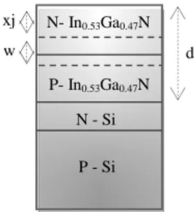
(2) F. Bouzid et al.. J Fundam Appl Sci. 2012, 4(1), 108-120. 109. A tandem cell using Indium Gallium Nitride (InxGa1-xN) for the top cell and Silicon (Si) for the bottom cell is advantageous in two respects: The direct bandgap of the InxGa1-xN alloy system, extends continuously from Indium Nitride (InN) bandgap which is 0.7eV in the medium infrared, to that of the Gallium Nitride (GaN) which is 3.42eV [2] in the near ultraviolet, makes the InxGa1-xN alloy a promising candidate for radiation and temperature resistant single or multi-junction solar cells [3]. In the other hand, Si is relatively cheap and plentiful and its processing techniques are well established, in addition to the fact that the Si bandgap of 1.1ev is ideally suited for the bottom junction of high efficiency two-junction solar cells [4]. In this paper, we have modelled the photovoltaic conversion efficiency of series-connected, two-junction, two-terminal InxGa1-xN on Si solar cells in terms of their physical parameters, employing a simulation program developed for this reason, where the InxGa1-xN has an alloy fraction close to In0.53Ga0.47N. 2. MODEL DESCRIPTION Figure 1 show a simplified structure of the In0.53Ga0.47N/Si tandem, where xj is the junction depth, w is the depletion region width and d is the cell thickness.. xj. N- In0.53Ga0.47N. w. d P- In0.53Ga0.47N N - Si P - Si. Fig.1. Simplified configuration of the In0.53Ga0.47N/Si tandem.. In this work, calculations were all performed under 1-sun AM1.5 illumination and a temperature of 300°k using the one diode ideal model, and for convenience, several simplifying assumptions were made, including no series resistance losses, no reflection losses and contact shadowing. Currents calculation follows the general methodology described in ref. [5]. 3. ANALYTICAL MODEL The total output current drawn from single cells under illumination is given by [5] as: I Total I Light I Dark. (1).
(3) F. Bouzid et al.. J Fundam Appl Sci. 2012, 4(1), 108-120. 110. λmax. I Light . I λ I λ I λdλ p. n. dr. (2). λmin. Where: Ip(λ) is the photocurrent due to holes collected at the depletion edge xj; In(λ) is the photocurrent due to electrons collected at the depletion edge xj+w; Idr(λ) is the contribution of the depletion region to the photocurrent; λ min is the wavelength corresponding for the bottom cell in case of double junction system to the top cell bandgap, and equals zero for the top cell; λmax is the wavelength corresponding to the cell bandgap. The dark current can be expressed as: I. Dark. I0. . qv exp kT 1 . (3). Where: I0 is the saturation current which was calculated following the method described in the ref. [5], v is the applied voltage, k is the Boltzmann constant and T is the temperature. The open circuit voltage is given by [5] as: V oc . kT Isc ln 1 q I0 . (4). Where Isc is the short circuit current. The open circuit voltage of the tandem is taken to be the sum of the open circuit voltages of the tandem junctions: n. V oc . v. oc, i. (5). i 1. Where n is the number of junctions incorporated in the tandem. The cell output power is given as: p I Total V. (6). The cell conversion efficiency is usually taken to be: η . Im Vm p inc. (7). Where Im and Vm are coordinates of the maximum power point, Pinc is the total incident solar power. The fill factor is defined by: FF . Im Vm I sc v oc. (8).
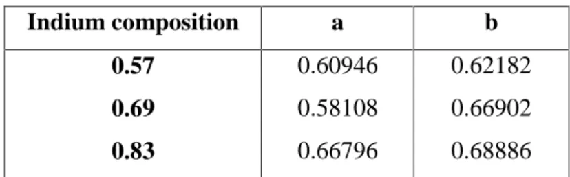
(4) F. Bouzid et al.. J Fundam Appl Sci. 2012, 4(1), 108-120. 111. InxGa1-xN parameter equations used in our program The equation relating the bandgap energy to the mole fraction x is given by [6,7] as: Eg(x)= x × Eg(InN) + (1-x) × Eg(GaN) – x × (1-x) × C. (9). Where: Eg(InN) = 0.7eV, Eg(GaN) = 3.42eV and C is a bowing parameter which is taken to be equal to 1.43. The electron and hole mobilities are calculated as a function of doping using [8]: μ i N μ min, i . μ max, i μ min, i. . 1 N N g, i. γi. (10). Where i represent either electrons (e) or holes (h), N is the doping concentration and the specific parameters µ min, µ max, γ and Ng are given in Table 1.. Table 1. Parameters used in the simulation of the InN and GaN carrier mobilities. µmin,e. µmax,e. µmin,h. µmax,h. [cm²/vs] [cm²/vs] [cm²/vs] [cm²/vs]. γe. γh. Ng,e. Ng,h. [cm-3]. [cm-3]. GaN. 55. 1000. 3. 170. 1. 2. 2e17. 3e17. InN. 30. 1100. 3. 340. 1. 2. 2e17. 3e17. InxGa1-xN electron mobilities are taken as a linear interpolation between the InN and GaN values; however, hole mobilities of the InxGa1-xN alloys are assumed to be similar to the GaN hole mobility. The absorption coefficient of the InxGa1-xN alloys is taken to be [9]: α E 10. 5. . a E Eg b E Eg. 2 cm. 1. (11). Where E is the incoming photon energy given in ev, a and b are dimensionless fitting parameters. The fitting parameters used in our program are shown in Table 2.. Table 2. Fitting parameters used to calculate the absorption coefficient of the In xGa1-xN alloys. Indium composition. a. b. 0.57. 0.60946. 0.62182. 0.69. 0.58108. 0.66902. 0.83. 0.66796. 0.68886.
(5) F. Bouzid et al.. J Fundam Appl Sci. 2012, 4(1), 108-120. 112. The relative dielectric constant for InN and GaN are 10.5 and 8.9 respectively [10,11], so a linear interpolation has been made to find the relative dielectric constant of the InxGa1-xN alloys. Effective masses for electrons and holes were determined using the following equations [12]: me*= m0 × (0.2 - 0.105 × x). (12). mh*= m0 × (1.25 + 0.8 × x). (13). Where m0 is the electron rest mass. Si parameter equations used in our program The equation relating the bandgap energy to the temperature is given by [13] as: E g T 1.17 . 4.73 10-4 T 2 636 T. (14). The electron and hole mobility components due to lattice scattering, ionized impurity scattering and carrier – carrier impurity scattering are calculated using the formula [14]: 1 μ. . tot e, h. 1 1 μ IL μc. (15). Where µ LI is the combined lattice and ionized impurity scattering mobility and µ c is the carrier – carrier impurity scattering mobility component.. μc . μ eLI . μ LI h . T 1.04 10 21 300 . 3 2. (16). T 1 3 n p ln 1 7.45 10 13 n p 300 2. 1. 1. T 1252 300 CI. -2.33. T 1.432 10 17 300 T 407 300 CI 2.67 10. 17. T 88 300 . - 0.57. T 54.3 300 . - 0.57. (17). 2.546. -2.23. T 300 . (18). 2.546. Where n, p and CI are the electron, hole and total ionized impurity concentrations respectively. For indirect transitions, light absorption is assisted by the absorption or emission of phonons. Theory predicts the absorption coefficient of crystalline Silicon to be [15]:.
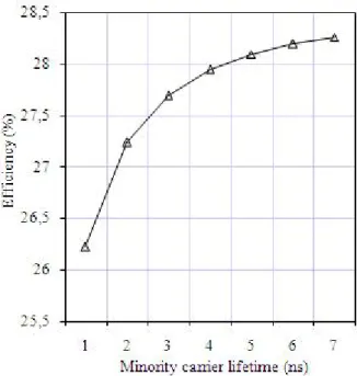
(6) F. Bouzid et al.. J Fundam Appl Sci. 2012, 4(1), 108-120. α T A j C i i, j1.2 . hν E g, j E ph, i hν E g, j E ph, i 2. E ph, i exp kT . 2. 1 . 1 exp . E ph, i kT. . Ad . 113. 32 hν E g, d . (19). hν. Where i and j are the phonons 1, 2 and band gaps 1, 2 respectively. Eg,1 = 1.16 [ev] and Eg,2 = 2.25 [ev] are the indirect band gaps 1 and 2 respectively, and Eg,d = 3.2 [ev] is the direct band gap 3 with all values for T being (0°K). Eph,1 = 212 × k and Eph,2 = 670 × k are the phonons with C1 = 5.5, C2 = 4, A1 = 253, A2 = 3312 and Ad = 2.3×10⁷ in [cm-1 ev-2]. The first term describes the absorption of phonons while the second describes the emission of phonons during absorption of light. The third term gives the absorption for a direct transition. 4. RESULTS AND DISCUSSION The analysis starts by assuming the physical and geometrical parameter values of the twojunctions presented in Table 3. Where Na and Nd are the acceptor and donor concentrations, Sh and Se are the recombination velocities in the N and P-type regions respectively.. Table 3. Physical and geometrical parameters used in simulations. Eg. Na -3. Nd -3. τe. τh. Se. Sh. xj. d. [ev]. [cm ]. [cm ]. [s]. [s]. [cm/s]. [cm/s]. [µm]. [µm]. In0.53Ga0.47N. 1.622. 1e17. 1e16. 4e-9. 4e-9. 1e3. 1e3. 2e-1. 3. Si. 1.125. 1e17. 1e16. 1e-6. 1e-6. 1e6. 1e6. 2e-1. 200. In0.53Ga0.47N minority carrier lifetimes effect on the conversion efficiency of the tandem. The minority carrier lifetime is one of the most critical parameters in determining the efficiency of a solar cell. We simulated the effect that lower lifetimes of the In0.53Ga0.47N top cell would have on device performance, and the results were shown in figure (2)..
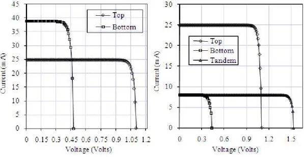
(7) F. Bouzid et al.. J Fundam Appl Sci. 2012, 4(1), 108-120. 114. Fig.2. Effect of minority carrier lifetimes of the In0.53Ga0.47N junction on the conversion efficiency of the tandem.. The large absorption coefficient in the direct bandgap In xGa1-xN alloys causes the majority of the electron-hole pairs to be generated less than a diffusion length away from the junction. So for short carrier lifetimes, the carriers recombine quickly what implies a reduction in the conversion efficiency. Hole lifetimes as high as 6.5ns and 5.4ns have been observed in GaN and InN respectively [16,17]. However, InxGa1-xN alloys are likely to have lower lifetimes due to compositional fluctuations, and therefore a 4ns minority carrier lifetime was assumed in our calculations for both electrons and holes.. Simulation of the current-voltage characteristics Figure (3) shows the current-voltage characteristic of the single junctions and that of the tandem, while Table 4 gives the computations of the open circuit voltage, short circuit current, fill factor and the conversion efficiency for the In0.53Ga0.47N/Si tandem..
(8) F. Bouzid et al.. J Fundam Appl Sci. 2012, 4(1), 108-120. 115. Fig.3. Simulated current-voltage characteristics of the In0.53Ga0.47N/Si tandem: (Left) for top and bottom single junctions, (Right) for top, bottom and the tandem.. Table 4. Photovoltaic parameters of the In0.53Ga0.47N/Si tandem.. Voc [V]. Isc [mA]. FF [%]. η [%]. Top cell: In0.53Ga0.47N. 1.10. 24.92. 88.93. 25.16. Single bottom cell: Si. 0.47. 38.94. 79.45. 15.17. Bottom cell: Si. 0.44. 07.94. 78.07. 02.77. Tandem: In0.53Ga0.47N / Si. 1.54. 07.94. 91.55. 27.94. According to the results represented in Table 4 and the preceding curves, one note that, the current-voltage curve of the top cell stayed the same, while the current-voltage curve of the bottom cell had a current drop. This current decrease was expected because the incident spectrum was diminished while crossing the top cell, and since the junctions are mechanically stacked in series, the overall current-voltage characteristic is limited in its current level by the characteristic with the lowest current. In addition, we note a significant increase in efficiency from single junctions to the tandem. Our calculations predict an efficiency of 27.94%, for the In0.53Ga0.47N/Si tandem by using realistic parameters. This result is very similar to that obtained by L. Hsu et al [4]. They calculated the conversion efficiency of InGaN/Si tandem cell, made from low quality.
(9) F. Bouzid et al.. J Fundam Appl Sci. 2012, 4(1), 108-120. 116. material, using a modified version of the standard equations for calculating the electrical characteristics of the tandem, using the air mass 1.5 global irradiance, and they obtained a conversion efficiency of about 27%. The differences in efficiency results can be partly attributed to the difference in parameter formulas used. All formulas seek to duplicate results from actual measurements. Therefore, all formulas are approximations only and it is difficult to state which formula is more correct. In0.53Ga0.47N carrier front recombination velocities effect on the conversion efficiency of the tandem In this work, the back surface recombination velocity was fixed at 1e3cm/s, and the influence of the front recombination velocity on the conversion efficiency has been simulated, where values of 1e3, 1e4, 1e5 and 1e6 cm/s was used.. Fig4. (Left) Simulated current-voltage characteristics of the In0.53Ga0.47N/Si tandem for various front recombination velocities, (Right) Effect of In0.53Ga0.47N front recombination velocities on the conversion efficiency of the tandem.. From figure 4 above, it is apparent that the conversion efficiency drops notably with increasing the front recombination velocity, since most of the photo-generated carriers cannot be collected by the electrodes what implies a low electric current. Therefore, to reduce the power loss, the front surface recombination velocity should not exceed 1e3cm/s..
(10) F. Bouzid et al.. J Fundam Appl Sci. 2012, 4(1), 108-120. 117. Effect of the bottom cell thickness on the conversion efficiency of the tandem It can be seen from Figure 5 below that the efficiency increases significantly with increasing the cell thickness.. Fig.5. Effect of the Si thickness on the conversion efficiency of the tandem.. The curve show an improvement from 25.53% to 27.94% for 5µm and 200µm Si cell thickness respectively for the reason that, in case of thin thickness, most of the incident photons are not absorbed resulting in a lower efficiency. So a cell thickness of about 200µm is needed to lose not too much of the efficiency. Effect of changing the operating temperature on the conversion efficiency of the tandem According to the results represented in table 5 and figures (6) and (7) below, it is seen that the increase of the cells temperature causes an increase in the reverse saturation current because of the reduction in bandgaps. Thus, the open circuit voltage will increase and the mechanism of carrier’s production becomes increasingly significant what implies a weak increase in the short circuit current..
(11) F. Bouzid et al.. J Fundam Appl Sci. 2012, 4(1), 108-120. 118. Table 5. Effect of temperature on the photovoltaic parameters.. T (°k). 300. 340. 380. Cell. Top. Bottom. Tandem. Top. Bottom. Tandem. Top. Bottom. Tandem. I0 (A). 7.62e-21. 3.94e-10. -. 1.79e-17. 1.39e-07. -. 8.55e-15. 1.5e-05. -. Voc (V). 01.10. 0.43. 01.54. 01.02. 0.32. 01.34. 0.94. 0.21. 01.15. Isc (mA). 24.92. 07.94. 07.94. 24.97. 08.03. 08.03. 25.02. 08.11. 08.11. FF (%). 88.93. 78.07. 91.55. 87.19. 70.88. 89.64. 85.16. 59.73. 87.27. η (%). 25.16. 02.77. 27.94. 22.92. 1.88. 24.80. 20.63. 01.03. 21.66. Fig.6. Current-voltage characteristics of the tandem for various Temperatures.. It may be seen also that the fill factor undergoes a reduction with the increase of the cells temperature following the increase in the dark saturation current, and owing to the fact that the reduction in the open circuit voltage is more significant with respect to the increase of the short circuit current, the conversion efficiency will also decrease..
(12) F. Bouzid et al.. J Fundam Appl Sci. 2012, 4(1), 108-120. 119. Fig.7. Effect of the temperature: (Left) on the open circuit voltage and the short circuit current, (Right) on the fill factor and the conversion efficiency of the tandem. 5. CONCLUSION In this study, we have improved a comprehensive model to predict the performance of double junction In0.53Ga0.47N/Si tandem cells under 1-sun AM1.5 illumination, using realistic parameters by a simulation program designed for this reason. It is found that higher values of the surface recombination velocity at the top In0.53Ga0.47N cell causes a considerable drop of the conversion efficiency. So, in order to achieve higher conversion efficiency, it is important to keep the front recombination velocity under 1e3cm/s. Moreover, a cell thickness of about 200µm is privileged to not contribute significantly in recombination. In addition, we have analyzed the effect of elevated operating temperature on the conversion efficiency and we found that the increase of the tandem’s temperature causes a degradation of their performance. 6. REFERENCES [1] Dhere R, Ramanathan K, Scharf J, Moutinho H, To B, Duda A, and Noufi R, Investigation of Cd1-xMgxTe Alloys for Tandem Solar Cell Applications. IEEE 4th World Conference on Photovoltaic Energy Conversion. 2006: May 7-12. [2] Rüdiger Q. 2008, Gallium Nitride Electronics, Springer-Verlag, Berlin Heidelberg. [3] Shen X, Lin S, Li F, Wie Y, Zhong S, Wan H, Li J, Simulation of the InGaN-based tandem solar cells. Photovoltaic Cell and Module Technologies II, Edited by Bolko von Roedern, Alan E. Delahoy, Proceedings of Spie, 2008: Vol. 7045-E..
(13) F. Bouzid et al.. J Fundam Appl Sci. 2012, 4(1), 108-120. 120. [4] Hsu L and Walukiewicz W, Modelling of InGaN/Si tandem solar cells. Journal of Applied Physics, 2008: 104, 024507. [5] Sze S. M. and Ng K. K. 2006, Physics of Semiconductor Devices, Third Edition, John Wiley, Interscience. [6] Wu J and Walukiewicz W, Bandgaps of InN and group III nitride alloys. Superlattice. Microst, 2003: 34, 63-75. [7] Wu J, When group III-nitrides go infrared: new properties and perspectives. Journal of Applied Physics, 2009: 106, 011101-1-28. [8] Mnatsakanov T. T, Levinshtein M. E, Pomortseva L. I, Yurkov S. N, Simin G. S, and Asif Khan M, Carrier mobility model for GaN. Solid-State Electron, 2003: 47, 111-115. [9] Muth J. F, Lee J. H, Shmagin I. K, Kolbas R. M, Caser H. C, Keller B. P, Mishra U. K and Den Baars S. P, Absorption coefficient, energy gap, exciton binding energy, and recombination lifetime of GaN obtained from transmission measurements. Applied Physics Letters, 1997: 71, 2572-2574. [10] Levinshtein M. E, Rumyantsev S. L and M. S. Shur. 2001, Properties of Advanced Semiconductor Materials: GaN, AlN, InN, BN, SiC, SiGe, John Wiley & Sons, NewYork. [11] Inushima T, Higashiwaki M and Matsui T, Optical properties of Si-doped InN grown on sapphire (0001). Physical Revue, 2003: B68, 235204-1-7. [12] Mohammad S. N, Salvador A. A and Morkoç H, Emerging Gallium Nitride Based Devices. Proceedings of the IEEE, 1995: Vol. 83(10), October. [13] Seraphin B. O. 1979, Topics in applied physics, Vol 31. Springer-Verlag. [14] Siegfried S. 1984, Analysis and simulation of semiconductor devices, Springer-Verlag. [15] Bucher K, Bruns J and Wagemann H. G, J. Appl. Phys, 1994: 75 (2), Jan. [16] Bandic Z. Z, Bridger P. M, Piquette E. C, Mc Gill T. C, Minority carrier diffusion length and lifetime in GaN. Applied Physics Letters, 1998: 72, 3166-3168. [17] Chen F, Cartwright A.N, Lu H, Schaff. W. J, Temperature dependence of carrier. lifetimes in InN. Applied Physics Letters, 2005: 87, 212104-1-3.. How to cite this article Bouzid F and Hamlaoui L. Investigation of InGaN/Si double junction tandem solar cells. J Fundam Appl Sci. 2012, 4(2), 108-120..
(14)
Figure

+3

Documents relatifs
Abstract: In this work, the solar power conversion efficiency of InGaN/Si double junction tandem solar cells was investigated under 1-sun AM1.5 illumination, using realistic
Les nombreuses salles de concert de Sofia sont toujours combles et l’on y voit des écoliers de dix à douze ans écouter avec ferveur les grands opéras d u
Comparing mono and multicrystalline solar cells with similar resistivities, and fabricated with process 2, this temperature coefficient is slightly lower for mc-Si solar cells
In the 1960s-1970s, the geometry of solar cells for terrestrial applications remained circular due to the high cost of silicon wafer fabrication.. However, while keeping a
Despite the complexity of disordered organic materials, Drift Diffusion based device simulation remains a powerful tool to analyze organic solar cells and
when the transparent bottom electrode is used as cathode, the contribution of fullerene to the Jsc short-circuit current of the cells, if not dominant, is not
Pore water MeHg concentrations in the small ‘upland wetland’ organic sediments averaged 0.28 ng-Hg l –1 , which is within the range of concentrations found in other
In § 2 we briefly review core assumptions in rele- vant literature on problem identification and formulation and problem solving. In § 3 , we introduce the concept of need and
