HAL Id: hal-00987365
https://hal.archives-ouvertes.fr/hal-00987365
Submitted on 6 May 2014
HAL is a multi-disciplinary open access
archive for the deposit and dissemination of
sci-entific research documents, whether they are
pub-lished or not. The documents may come from
teaching and research institutions in France or
abroad, or from public or private research centers.
L’archive ouverte pluridisciplinaire HAL, est
destinée au dépôt et à la diffusion de documents
scientifiques de niveau recherche, publiés ou non,
émanant des établissements d’enseignement et de
recherche français ou étrangers, des laboratoires
publics ou privés.
A Defect-tolerant Cluster in a Mesh SRAM-based
FPGA
Arwa Ben Dhia, Saif Ur Rehman, Adrien Blanchardon, Lirida Naviner,
Mounir Benabdenbi, Roselyne Chotin-Avot, Habib Mehrez, Emna Amouri,
Zied Marrakchi
To cite this version:
Arwa Ben Dhia, Saif Ur Rehman, Adrien Blanchardon, Lirida Naviner, Mounir Benabdenbi, et
al.. A Defect-tolerant Cluster in a Mesh SRAM-based FPGA. International Conference on
Field-Programmable Technology (FPT), Dec 2013, Kyoto, Japan. pp.434-437, �10.1109/FPT.2013.6718407�.
�hal-00987365�
A Defect-tolerant Cluster in a Mesh SRAM-based
FPGA
Arwa Ben Dhia
∗, Saif Ur Rehman
†, Adrien Blanchardon
‡, Lirida Naviner
∗, Mounir Benabdenbi
†,
Roselyne Chotin-Avot
‡, Habib Mehrez
‡, Emna Amouri
‡, and Zied Marrakchi
§∗ Institut TELECOM, TELECOM ParisTech, Paris, France †Grenoble-Alpes University, TIMA Laboratory, Grenoble, France
‡LIP6, Pierre and Marie Curie University, Paris, France §FLEXRAS Technologies, Saint-Denis, France
Abstract—In this paper, we propose the implementation of multiple defect-tolerant techniques on an SRAM-based FPGA. These techniques include redundancy at both the logic block and intra-cluster interconnect. In the logic block, redundancy is implemented at the multiplexer level. Its efficiency is analyzed by injecting a single defect at the output of a multiplexer, considering all possible locations and input combinations. While at the interconnect level, fine grain redundancy is introduced which not only bypasses defects but also increases routability. Taking advantage of the sparse intra-cluster interconnect struc-tures, routability is further improved by efficient distribution of feedback paths allowing more flexibility in the connections among logic blocks. Emulation results show a significant improvement of about 15% and 34% in the robustness of logic block and intra-cluster interconnect respectively. Furthermore, the impact of these hardening schemes on the testability of the FPGA cluster for manufacturing defects is also investigated in terms of maximum achievable fault coverage and the respective cost.
I. INTRODUCTION
The increasing integration density according to Moore’s law is being slowed due to economic and physical limits. As yield goes down, one of the future challenges is to find a way to use a maximum of fabricated circuits while tolerating physical defects spread all over the chip. With respect to the defect tolerance, FPGAs have attained a central focus due to their reconfigurability which enables to bypass the defective areas and implement the application on defect-free resources. In the technical literature, there are several techniques for repairing FPGAs when they are affected by permanent faults. Most of these hardening schemes resort to redundancy and can be classified into software-based and hardware-based techniques. Software-based techniques avoid defective resources by means of place-and-route tools which map around the defects [1]. Hence, the efficiency of the software approaches rely on the performance of such tools. Hardware-based techniques employ modifications in the basic architecture. In some cases, extra hardware resources are added, providing redundancy at different granularity levels. While in some cases, architecture optimization is done to automate the configuration bits shift mechanism [2].
Mesh architectures are the most common in academic [3] and commercial FPGAs [4], because of the simplicity of their physical layout. Logic blocks are typically arranged in
a grid and are surrounded by horizontal and vertical routing channels. The routing fabric consists of wiring segments and programmable switches organized into rows and columns. The set of switches used to connect a logic block to an adjacent routing channel is called a connection block. Most of the FPGA area is occupied by routing resources whose programmable switches increase the signal propagation delay [5]. Hence, in order to reduce the interconnect resources, modern FPGAs gather logic blocks into clusters [6]. Moreover, the cluster interconnect structure can be depopulated by using sparse rather than full crossbars [7]. Connection blocks can be avoided by connecting clusters directly to switch boxes [8].
In [9], we present a mesh of clusters FPGA, where a depopulated cluster is directly connected to the surrounding switch boxes. We take this cluster as a reference and the starting point of all the studies that will be undertaken in this paper, as it combines all the aforementioned possibilities of reducing the FPGA interconnect network.
In this paper, we present different defect-tolerant schemes applied at different levels in the cluster of a mesh FPGA. These defect-tolerant schemes are classified as logic and intra-cluster interconnect level redundancy. At the logic level, an exclusive Butterfly design is incorporated which involves the modifi-cation of basic Look-Up Table (LUT), whereas the schemes applied at intra-cluster interconnect incur redundancy at a wire as well as switch level of the crossbar structure. The main goal is to analyze these schemes with respect to the degree of their defect tolerance and their impact on the routability and testability of the cluster architecture. Results are produced for the FPGA cluster enriched with each scheme separately as well as for all the schemes applied simultaneously on the cluster.
The remainder of this paper is organized as follows. Section II describes the hardening techniques we used to increase the cluster robustness and routability. Emulation/simulation results for defect tolerance, routability and testability are presented in section III. Finally, conclusion is drawn in Section IV.
II. HARDENING THECLUSTER
A. Redundancy in the logic blocks
We adopted the architecture called Butterfly in its modified version described in [10]. Such architecture is more robust
than the conventional LUT, and requires a TMR voter after the last stage of Mux2s. We used the TMR voter introduced in [11], which is tolerant to single faults.
B. Redundancy in the interconnect blocks
1) Fine-Grain Redundancy (FGR): In this work, we use the Fine-Grain Redundancy (FGR) introduced in [12] at the intra-cluster interconnect.
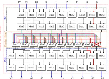
In the crossbars ‘Up’ and ‘Down’, four levels of Mux2s are added: two levels of upstream Mux2s to avoid the defect by shifting the signal, and two other downstream levels to restore the signal. Figure 1 depicts a crossbar ‘Down’ hardened with FGR technique. The crossed Mux2 in the figure represents a defective Mux2. It was meant to connect the input I5 to the output O8. The upstream FGR allows to re-route the I5 signal to the neighbouring Mux2. Then, the downstream FGR allows to restore the signal that will be connected to O8. Nonetheless, the I5 signal can be re-routed only if the neighbouring Mux2 is a spare resource. Crossbar ‘Down’ FGR O4 O5 O6 O7 O8 O9 O3 O2 O1 O0 FGR I5 I4 I3 I2 I1 I0 C0 C1 C2
Crossbar ‘Down’ with FGR
Mux2 Mux2 Mux2 Mux2 Mux2 Mux2 Mux2 Mux2 Mux2 Mux2
Mux2 Mux2 Mux2 Mux2 Mux2 Mux2 Mux2 Mux2 Mux2 Mux2 Mux2 Mux2 Mux2 Mux2 Mux2 Mux2 Mux2 Mux2 Mux2 Mux2
Mux2 Mux2 Mux2 Mux2 Mux2 Mux2 Mux2 Mux2 Mux2 Mux2 Mux2 Mux2 Mux2 Mux2 Mux2 Mux2 Mux2 Mux2
Fig. 1: Crossbar ‘Down’ hardened with FGR technique
2) Distributed Feedbacks (DF): Among the cluster’s twelve outputs, eight are fedback in pairs to the ‘Down’ linking block (the four crossbars ‘Down’), and the four other outputs (drawn in thick blue line in Fig. 2) are fedback to all crossbars ‘Down’. We call them Distributed Feedbacks (DF).
In fact, in the initial cluster architecture, if a feedback signal happens to be routed by a defective Mux2 in the crossbar ‘Down’, the connection will not be possible. However, with the DF technique, the connection can be made via another Crossbar ‘Down’. That is how a defect can be bypassed. Thanks to the DF technique, the possibility to route the same signal is multiplied by 4. As a result, the number of inputs per crossbar ‘Down’ increases, as well as the size of all multiplexers.
Like in the aforementioned FGR approach, a defect map is required to bypass the defects. While configuring the FPGA, the defective Mux2s inside the crossbar ‘Down’ are bypassed and all the feedbacks are routed to the other defect-free Mux2s.
The DF method is focused on the improvement of connectivity within a cluster between logic blocks.
‘Up’ Crossbar Local Interconnect 24 inputs CLB CLB CLB CLB CLB CLB CLB CLB CLB CLB 12 outputs Crossbar ‘Down’ Crossbar ‘Down’ Crossbar ‘Down’ Crossbar ‘Down’ 10 10 10 10
Fig. 2: Structure of a mesh cluster with Distributed Feedbacks
III. DEFECTTOLERANCE, ROUTABILITY AND
TESTABILITY OF THECLUSTER
In this section, the impact of the aforementioned techniques on the defect tolerance, routability and testability of the cluster is presented. Moreover, similar results for a cluster combinedly enriched with all these techniques are also analyzed.
Two assumptions were considered througout the analyses. First, the cluster inputs are fault-free, since our target is to analyze the cluster’s inherent defect tolerance. Second, configuration memory is protected against defects by using error detecting/correcting codes [13].
The designs under study are: the cluster architecture as de-scribed in [9] (initial version), the one enriched with Butterfly CLBs in the logic block, the one enriched with FGR in the ‘Down’ and ‘Up’ linking blocks, the one enriched with DF, and the one enriched with all hardening techniques mentioned above.
A. Defect tolerance
Defect tolerance is referred to the design’s inherent robust-ness against a defect. As a matter of fact, for some input conditions, failures caused by a defect within the cluster appear in a non-sensitized path and thus can not propagate to the output. This phenomenon is referred to as logical masking. As a robustness metric for our study, we resort to logical masking. 1) Methodology: A defect is modeled by a stuck-at 0/1 at the output of a Mux2, and any Mux2 in the CLBs or crossbars can be defective. Fault injection is achieved through a platform that considers all possible input combinations and all possible locations of a single defect in a given design. Actually, the platform returns the number of logical maskings. To get the logical masking rates, the number of logical maskings is normalized by the total number of tests.
2) Emulation results: Table I shows the emulation results in terms of logical masking rates for all the cluster architectures explored in this work. It is worth noting that the use of the Butterfly structure rendered the cluster CLBs completely
TABLE I: Logical masking emulation results.
Cluster architecture
Logical masking per block(%)
‘Down’ Logic ‘Up’
Initial 100 85.33 55.55
With Butterfly 100 100 55.55
With FGR 100 85.33 84.21
With DF 100 85.33 55.55
With Butterfly, FGR and DF 100 100 84.21
TABLE II: Defect avoidance and routability results.
Cluster Architecture Total of Mux2s Number of bypassed Mux2s Increase of cluster area (%) Routable with one defect Initial 588 0 0 NO With DF 708 33 20.4 YES With FGR 784 36 33.3 YES
With FGR and DF 928 77 57.8 YES
tolerant to single defects. And thanks to the use of FGR in the interconnect blocks, logical masking rate was increased by roughly 30%.
Combining both hardening techniques enables to take ad-vantage of the two gains in logical masking, but at the expense of area overhead. Indeed, employing FGR in the ‘Down’ linking block is seemingly pointless as long as the ‘Down’ crossbars are already 100% robust against single defects. And the same remark can be made for the DF technique. Nevertheless, FGR in the ‘Down’ linking block is useful from a routability and defect bypassing viewpoint. So is the DF technique. This will be explained in the next subsection. B. Routability and Defect avoidance
Routability of an FPGA is defined by the number of routing solutions it offers for an application to be mapped on it. Higher routability makes it easier to bypass the defects by providing spare resources.
1) Methodology: A defect, modeled by an Undefined value at the Mux2 output in Modelsim, is injected within the crossbar ‘Down’, which makes the cluster unusable. Then, the cluster is reconfigured to use either spare connections inside the defective crossbar thanks to FGR or another crossbar ‘Down’ thanks to DF. Hence, the defective Mux2 is bypassed and the cluster functionality is restored.
Since the inner architecture of the logic blocks has no im-pact on routability and defect avoidance, it is useless analyzing the Butterfly structure in this subsection.
2) Simulation results: Table II shows the maximum number of defective Mux2s that can be bypassed for each cluster design and the area overhead with respect to the initial architecture.
As far as the architecture with DF is concerned, it is possible to increase the number of distributed feedbacks but this would increase the cluster area by more than 20.4%. Moreover, it is worth noticing that DF and FGR allow to bypass virtually the
Fig. 3: Comparison of fault coverage for the cluster with Butterfly, FGR and DF
same number of Mux2s (33 for the DF versus 36 for the FGR which represents a gain of only 0.5% in the overall cluster). However, FGR causes about 13% of additional area overhead as compared to DF. Thus, if solely one hardening technique had to be used in the interconnect blocks, one would elect the DF over the FGR.
DF and FGR techniques can be used together in the cluster which allows to bypass 77 Mux2s, that is more than the sum of bypassed Mux2s in the architectures using either FGR (36 bypassed Mux2s) or DF (33 bypassed Mux2s), but the cluster area is then increased by more than the sum of the overheads. C. Testability
To scale the efficiency and performance of the defect toler-ant schemes, testability of the given architectures is calculated in terms of fault coverage which is defined as a ratio between detected faults and the total number of potential faults in the given circuit. The other metrics of testability include test time and the number of corresponding test vectors.
1) Methodology: To analyze the testability aspects of the cluster architecture, internal scan design is utilized which is the most popular Design For Testability (DFT) technique [14]. To incorporate the testing mechanism in the cluster architectures, multiplexed Flip-Flop scan style is used and single scan chain is inserted which serially connects all CLBs of the cluster.
In this experiment, metrics of testability such as fault cov-erage and test cost are determined for each cluster architecture using an Automatic Test Pattern Generation (ATPG) tool. To generate the test patterns, deterministic algorithm is used which is based on path sensitization mechanism in which a vector is generated and a complete set of faults on the path activated by this vector is detected. In our case, it requires a sequence of test vectors to activate and propagate the targeted fault in sequential logic. However, it is assumed that for a particular test vector, no other fault masks the targeted fault such that it cannot be detected.
2) Simulation results: The effect of each hardening tech-nique on the testability of the cluster is analyzed. For this purpose, stuck-at fault model is considered to determine the test and fault coverage. Faults are injected at gate level and the metrics of testability are measured for dominant faults.
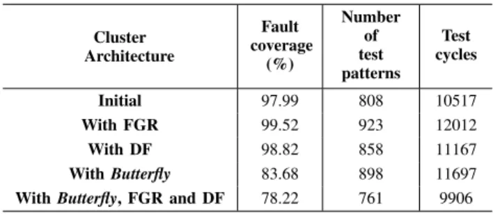
TABLE III: Testability metrics. Cluster Architecture Fault coverage (%) Number of test patterns Test cycles Initial 97.99 808 10517 With FGR 99.52 923 12012 With DF 98.82 858 11167 With Butterfly 83.68 898 11697
With Butterfly, FGR and DF 78.22 761 9906
Figure 3 depicts a comparison of the fault coverage and the respective test cost attained for different cluster architectures considered in this paper. In the plot, fault coverage curves of FGR and DF techniques shot up at the beginning as the large number of faults are detected with a fewer number of test patterns, thanks to the deterministic algorithm of pattern generator. Later on, the ratio of the number of detected faults to the number of required test patterns decreases which gives a relatively slower increase in fault coverage. In other words, for a limited period of test time, high density of detected faults at the beginning is favourable.
FGR and DF, both techniques give considerably high fault coverage. However, FGR dominates if test cost and robustness is taken into consideration. Table III shows the summary of the testability metrics for each hardening technique where the maximum achievable fault coverage and the respective number of required test patterns are given. Although feedback paths make fault detection costly in terms of computational time for test pattern generation as well as the number of required test patterns, DF technique gives a better trade-off in terms of testability. For approximately the same fault coverage, DF costs 7% less test time as compared to FGR. The main reason for this concession is the addition of potential nodes and devices in case of FGR which dramatically increases the number of faulty sites. The reason for the lower fault coverage in case of BF is the requirement of high computational effort to generate effective test patterns such that faults at the LUT can be propagated through the complex Butterfly structure, which in turn requires large number of test cycles for relatively lower number of injected faults as compared to DF or FGR. Similar is the case with architecture where all above mentioned hardening schemes are combined.
IV. CONCLUSION ANDFUTUREWORK
This paper presents different defect-tolerant schemes aiming at different levels in the cluster of an FPGA. At logic level, Butterfly design is used to enhance the logical masking up to 100% at the expense of 21% increase in cluster area and about 14% reduction in testability whereas, at the intra-cluster inter-connect level, Fine Grain Redundancy (FGR) and Distributed Feedback (DF) schemes are applied. Results have shown that FGR at intra-cluster interconnect improves logical masking to about 84% and testability to 99.5% respectively, giving an increment of 33.3% and 12.5% in cluster area and test
cost respectively. DF does not improve any logical masking. However, increase in routability improves the testability to 98.8% at the cost of 5.8% as compared to the initial cluster architecture. By combining all the defect-tolerant schemes (BF at logic, DF and FGR at interconnect level), the cluster can be made more robust to the permanent faults as it gathers all the pros of logical masking but at the expense of area overhead of 78.23% and testability degradation of 21%.
Future work includes the analysis of defect tolerance for switch box of the FPGA along with the cluster. We plan to extend this study for multiple manufacturing defects using other models like bridging and delay faults.
ACKNOWLEDGMENT
This work is a part of the project Robust FPGA ANR 11 INS-02, funded by The French National Research Agency and The Pole Systematic.
REFERENCES
[1] W.-J. Huang and E. McCluskey, “Column-based precompiled configu-ration technique for FPGA fault tolerance,” IEEE Field Programmable Custom Computing Machines Symp., 2001.
[2] A. Doumar, S. Kaneko, and H. Ito, “Defect and fault tolerance FPGAs by shifting the configuration data,” IEEE Defect and Fault-Tolerance Symp., pp. 377–385, 1999.
[3] V. Betz, J. Rose, and A. Marquardt, Architecture and CAD for
Deep-Submicron FPGAs. Kluwer Academic Publishers, January 1999.
[4] Altera. FPGA - field-programmable gate array. [Online]. Available: http: //www.altera.com/devices/fpga/stratix-fpgas/stratix10/stx10-index.jsp [5] Z. Marrakchi, H. Mrabet, and H. Mehrez, “Optimized local interconnect
for cluster-based mesh FPGA architecture,” in Microelectronics, 2008. ICM 2008. International Conference on, dec. 2008, pp. 15 –18. [6] D. Lewis, E. Ahmed, G. Baeckler, V. Betz, M. Bourgeault, D. Cashman,
D. Galloway, M. Hutton, C. Lane, A. Lee, P. Leventis, S. Marquardt, C. McClintock, K. Padalia, B. Pedersen, G. Powell, B. Ratchev, S. Reddy, J. Schleicher, K. Stevens, R. Yuan, R. Cliff, and J. Rose, “The Stratix II logic and routing architecture,” in Proceedings of the 2005 ACM/SIGDA 13th international symposium on Field-programmable gate
arrays, ser. FPGA ’05. New York, NY, USA: ACM, 2005, pp. 14–20.
[7] W. Feng and S. Kaptanoglu, “Designing efficient input interconnect blocks for LUT clusters using counting and entropy,” ACM Trans. Reconfigurable Technol. Syst., vol. 1, no. 1, pp. 6:1–6:28, Mar. 2008. [8] Z. Marrakchi, H. Mrabet, and H. Mehrez, “Programmable gate array,
switch box and logic unit for such an array,” Patent 7 795 911, Septem-ber, 2010.
[9] A. Ben Dhia, L. Naviner, and P. Matherat, “Analyzing and alleviating the impact of errors on an SRAM-based FPGA cluster,” in On-Line Testing Symposium (IOLTS), 2012 IEEE 18th International, june 2012. [10] A. Dhia, L. Naviner, and P. Matherat, “Comparison of Fault-Tolerant Fabless CLBs in SRAM-based FPGAs,” in IEEE Latin American Test Workshop (LATW), april 2013.
[11] T. Ban and L. de Barros Naviner, “A simple fault-tolerant digital voter circuit in TMR nanoarchitectures,” in NEWCAS Conference (NEWCAS), 2010 8th IEEE International, june 2010.
[12] A. Yu and G. Lemieux, “Defect-tolerant FPGA switch block and connection block with fine-grain redundancy for yield enhancement,” IEEE Field Programmable Logic and Applications Proc., 2005. [13] F. Monteiro, S. Piestrak, H. Jaber, and A. Dandache, “Fault-secure
interface between fault-tolerant RAM and transmission channel using systematic cyclic codes,” in On-Line Testing Symposium, 2007. IOLTS 07. 13th IEEE International, july 2007, pp. 199 –200.
[14] L.-T. Wang, C.-W. Wu, and X. Wen, VLSI Test Principles and
Architec-tures: Design for Testability (Systems on Silicon). San Francisco, CA,