HAL Id: hal-02005747
https://hal.archives-ouvertes.fr/hal-02005747
Submitted on 11 Jan 2021
HAL is a multi-disciplinary open access
archive for the deposit and dissemination of
sci-entific research documents, whether they are
pub-lished or not. The documents may come from
teaching and research institutions in France or
abroad, or from public or private research centers.
L’archive ouverte pluridisciplinaire HAL, est
destinée au dépôt et à la diffusion de documents
scientifiques de niveau recherche, publiés ou non,
émanant des établissements d’enseignement et de
recherche français ou étrangers, des laboratoires
publics ou privés.
Numerical Simulations for Sensitivity Analysis of the
Electrostatic Force Curve on Charge Localization in 3D
Menouar Azib, Fulbert Baudoin, Christina Villeneuve-Faure, G. Teyssedre,
Nicolas Binaud, Florian Bugarin, Stéphane Segonds
To cite this version:
Menouar Azib, Fulbert Baudoin, Christina Villeneuve-Faure, G. Teyssedre, Nicolas Binaud, et al..
Numerical Simulations for Sensitivity Analysis of the Electrostatic Force Curve on Charge Localization
in 3D. 2018 IEEE 2nd International Conference on Dielectrics (ICD), Jul 2018, Budapest, Hungary.
pp.1-4, �10.1109/ICD.2018.8514685�. �hal-02005747�
Numerical Simulations for Sensitivity Analysis of the
Electrostatic Force Curve on Charge Localization in 3D
M. Azib, F. Baudoin, C. Villeneuve-Faure and G.
Teyssedre
Laplace, Toulouse University, CNRS, INPT, UPS Toulouse, France
N. Binaud, F. Bugarin and S. Segonds
ICA, University Paul SabatierToulouse, France
Abstract—In the present work we present a model for Atomic
Force Microscopy (AFM) tip interacting electrostatically with a thin dielectric layer. Numerical simulations enabled us to estimate the electrostatic force induced by a half-ellipsoid charge distribution. The sensitivity of the shape of the Electrostatic Force Distance Curves (EFDC) to charge localization is investigated for the charge parameters as radius, depth and density of charges.
Keywords—AFM; space charge localization; thin dielectric films; numerical simulations
I. INTRODUCTION
The electrostatic force due to the interaction of electric charges is the fundamental force that is best understood, and it has been studied and verified experimentally with highest precision. As electrostatic forces govern most physical and chemical processes, their control at sub micrometer scale is of relevant importance for the development of nanotechnology, so as to build operative devices such as electronic components destined to the computer modern industry. Part of the progress achieved over the last decades has been driven by the development of Scanning Probe Microscopy (SPM) [1] and in particular Atomic Force Microscopy (AFM) [2]. Dielectric materials regularly take part of nanotechnology engineering as important components of electronic devices with thicknesses of the order 10 to 500 nm. Understanding the behavior of dielectric materials under different kinds of stress (electrical, thermal, etc.) is required to guarantee the reliability of the electronic devices. This is why; electrical modes derived from AFM [3-8] have been more and more used to probe the electrical properties of insulating materials at small scale. In these techniques, a metalized silicon probe composed by tip and cantilever is used to scan a thin dielectric fixed on a conducting surface. When a potential difference appears between the tip and the underlying metallic surface, an electrostatic force appears between the both. Moreover, as electrostatic force has a long-range character and it is stronger than the short-range forces such as the Van der Waals forces, topographic and local electrical properties as surface potential or permittivity could be measured simultaneously.
Charge injected in dielectric layer induced electrostatic force and consequently could be probed by electric modes derived from AFM. The first mode which was used is the Electrostatic Force Microscopy (EFM) [3-4]. In general cases of EFM, a bias voltage is applied between the AFM probe and
the sample, this bias voltage induces an electric field which is related to charge distribution in the dielectric by the first Maxwell's equation. The tip is submitted to an electrostatic force proportional to the capacitance and depends critically on tip-sample distance. By applying this method, it is possible to image charges with sub-micrometric lateral resolution [5]. However, the real issue of the EFM method is sensitivity to image charges which is critical to evaluate the amount of injected charge. To overcome this issue, the Kelvin Probe Force Microscopy (KPFM) [6-8] is used. KPFM measures with sub-micrometric lateral resolution the surface potential induced by charges stored in dielectrics. According to, hypothesis about charge distribution in surface or volume charge density can be estimated from KPFM measurements [8]. However, a lack of information about the in-depth position of charges limits its application for space charge detection.
For space charge detection in thin dielectric layers a new approach called EFDC (Electrostatic Force Distance Curve) [9] attempts to exploit the electrostatic force tip-sample distance curve obtained by the Force Distance Curve (FDC) [10] technique to get accurate information about the distribution in 3D of charges stored in a dielectric. As for KPFM and EFM, modelling of the electrostatic force between the AFM probe and the sample as a function of tip-sample distance is necessary. Various methods were developed, not always analytical [4, 11-13], even for highly simplified geometry, and numerical methods [14-17] are preferred. The limitations of these methods come from the simplification of the geometry of the system as well as hypotheses on the position of charges. These models are consistent with experimental result in restricted ranges of distances. A sophisticated model with an accurate geometry of the tip was proposed [18] in which a three dimensional model was developed: the electrostatic tip model provides an estimation of the electrostatic force between the tip and a dielectric layer free from charges. However, in this approach the tilt angle of the AFM tip was not considered. Recently, we have proposed a model [19] using the same geometry with taking into accounts the tilted angle and optimizing the mesh to cut down the computational time. To give more credit to this approach, the model estimates the electrostatic force over a buried electrode embedded in thin dielectric layer. Hence, the electrostatic force sensibility to potential distribution was investigated. The EFDC sensitivity to the potential distribution in 3D is highlighted.
The objective in the present work is to propose a model based on the same geometry introduced in previous studies [18-19], in order to study theoretically the electrostatic force sensibility to charge localization. The next sections present the tip-dielectric model and the sensibility of the tip to charge localization.
II. ELECTROSTATIC TIP MODEL
A. Geometry construction
Our general approach is to calculate the electrostatic force exerted on a stationary tip as a function of its vertical position over an infinite dielectric layer. The modeled layer is silicon nitride (SiNx) of thickness z = 500 nm and relative
permittivity = 7.5. The injected charges into the dielectric layer are described as a half-ellipsoid cloud of uniform charge density ρ, with a radius r and a depth d, cf. Fig. 1. The tip is modelled by the most representative shape [19]: a spherical-tetrahedral shape with tip apex of 25 nm, tip tetrahedron half-angle of 20° and tip height of 10 µm, in order to match to the shape of a real tip. An air domain with dimensions large enough to avoid edge effects is surrounding the tip and is in contact with the dielectric surface.
To compute the electrostatic force exerted on the tip induced by the charge distribution stored in the dielectric layer, we need to determine the electrostatic potential distribution V in the air box and the dielectric layer. This requires the resolution of the Poisson’s equation (Eq. 1) over the domain Ω, taking into account the boundary conditions on the interface Γ (see Fig. 1). Γ is composed of three parts Γ0, Γ1 and Γ2. The
problem is written as follows:
div (-ε grad(V)) = ρ in Ω (1)
V = 0 on Γ0 and Γ1 (2)
= 0 on Γ2 (3)
where ρ is the charge density distribution, n is the normal vector to the surface and ε is the permittivity of the dielectric or the air. The tip surface and the back side of the dielectric are set to the ground. In order to solve numerically the Poisson’s equation in the domain Ω and to determine the electrostatic force, the Finite Element Method (FEM) has been applied for
discretizing the geometry. As explained about mesh construction and optimization in [19], the regions where the electrostatic interactions are very high (around the apex) need to be meshed finely and the ones representing weak interactions are meshed more coarsely. Thus, we have added a domain without any boundary condition around the apex to mesh very finely this area.
The electrostatic force F acting on the tip surface was computed by the integration of the built-in Maxwell-stress-tensor, Mt, over all faces of the tip:
Mt = ‖ ‖ (4)
= Mt. . ds (5)
Where E is the electric field.
In order to study the electrostatic force sensitivity to charge localization we have modified successively the values of each charge parameters: the density ρ, the radius r and the depth d, then determine their variation impact on the force curve shape. The force curve is characterized by two parameters: (i) a maximum of the electrostatic force Fmax, which is reached on D = 0 nm (contact point between tip and dielectric); (ii) a curvature which is representative to curve shape [9].
B. Electrostatic force sensitivity to charge density
Fig. 2a represents the electrostatic force distance curves computed for different densities of charge ρ (r and d are fixed). This figure shows clearly that the electrostatic force is strongly influenced by the density of charges stored in the dielectric layer. Indeed, when the charge density increases the maximum of electrostatic force increases too. A variation by a factor of 1.5 on the charge density, i.e. from 10 000 C.m-3 to 15 000
C.m-3, leads to a variation on the maximum force by a factor of
2, from 0.39 nN to 0.81 nN. Fig. 2b plots out the ratio of the electrostatic force over the maximum of force for each density. The results reveal that the charge density variation does not modify the curvature of the EFDC curves. The shape of the EFDC is rigorously independent from the charge amount.
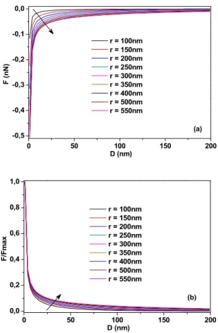
C. Electrostatic force sensitivity to radius of charge
Fig. 3a presents the variation of the EFDC as a function of radius r (ranging from 100 nm to 550 nm) at charge depth d fixed to 100 nm and density ρ fixed to 105 C.m-3. From this
figure, it can be readily seen that when the radius increases, the maximum of force increases too. For example, the maximum force for radius 100 nm and 500 nm is respectively 0.115 nN and 0.47 nN. Fig. 3b shows the normalized force curves for different charge cloud radii. The lateral spreading of charges affects not only the maximum of force but also the curvature. The curvature is more important for smaller values of charge cloud radius. Higher values of the curvature correspond to situations where the charges are highly localized (small radius) to the surface. With charges localized on small spots, a sharp distance dependence of the electrostatic force is obtained. Contrarily, when the charges spread laterally over the surface (larger values of r), a smooth curve is obtained and the baseline
is far from the maximum of force, due to the contribution of charges at different points from the surface and accordingly the curvature is lower.
D. Electrostatic force sensitivity to in-depth position of charges
Fig. 4a and Fig. 4b represent the influence of the in-depth distribution of charges on the force curve shape. The in-depth distribution of charges influences only the maximum force of the EFDC curve. The maximum force increases with increasing the height of the charge cloud, while the curvature remains nearly the same. Up to now it has not been possible to identify the relationship between the in-depth position of charges and the shape of the electrostatic force curve. One of the reasons in the computations reported here can be that the EFDC shape is dominated by the upper charge layers. Also, the sports are relatively broad in respect to the height in such a way that the effect of the in-depth position is smoothed. Certainly working with smaller charge clusters positioned at different depths could unravel some of the trends. However, our results are highly relevant in the context of the sensitivity of electrostatic force toward the in-depth of charge in the sample, as they demonstrate qualitatively the direct link between the both.
The result of this work adds some precise information about the electrostatic force curve sensitivity to charge localization against the experiment work [9] but relative contribution of density and spatial distribution of charge was not clearly identified. However, from experimental data, it was conjectured that the curvature of the EFDC is modified by the quantity of charges. However, the quantity of charge depends on the charge density, and on the width and depth of the charge cloud. With the ellipsoid shape taken here, the mathematical relation which links the quantity of charge Q to those parameters is described by the following equation:
Q = ρ
×
( × ××
) (6)Therefore, saying that the curvature is modified by the quantity of charge Q is futher generalised, while our results are very consistent in a way we could extract the individual effect of each parameter on the force curve. This is why special care should be given to the measurement interpretations, and numerical simulations are necessary steps in providing a full understanding of EFDC, identifying the influence of parameters and evaluating the performances of EFDC towards space charge probing.
0 50 100 150 200 -0,8 -0,6 -0,4 -0,2 F ( n N ) D (nm) ρ = 10 000 C.m-3 ρ = 11 000 C.m-3 ρ = 12 000 C.m-3 ρ = 13 000 C.m-3 ρ = 14 000 C.m-3 ρ = 15 000 C.m-3 (a) 0 50 100 150 200 0,0 0,2 0,4 0,6 0,8 1,0 ρ = 10 000 C.m-3 ρ = 11 000 C.m-3 ρ = 12 000 C.m-3 ρ = 13 000 C.m-3 ρ = 14 000 C.m-3 ρ = 15 000 C.m-3 F/ F m a x D (nm) (b)
Fig. 2. (a) The electrostatic force F as function of tip-sample distance D, (b) the ratio of F over the maximum force (Fmax) as a function of D, for different values of charge density ρ, the depth d and the radius r of the charge cloud were respectively fixed at 100 nm and 250 nm.
0 50 100 150 200 -0,5 -0,4 -0,3 -0,2 -0,1 0,0 r = 100nm r = 150nm r = 200nm r = 250nm r = 300nm r = 350nm r = 400nm r = 500nm r = 550nm F ( n N ) D (nm) (a) 0 50 100 150 200 0,0 0,2 0,4 0,6 0,8 1,0 r = 100nm r = 150nm r = 200nm r = 250nm r = 300nm r = 350nm r = 400nm r = 500nm r = 550nm F/ Fm a x D (nm) (b) Fig. 3. (a) The electrostatic force F as function of the tip-sample distance D, (b) the ratio of F over the maximum force (Fmax) as a function of D, for different values of the charge’s radius, the depth and the density of charges were respectively fixed at 100 nm and 105 C.m-3.
III. CONCLUSION AND PERSPECTIVE
In summary, the sensitivity of electrostatic force interactions between the AFM tip and a dielectric thin film, to charge distribution has been studied accurately using numerical simulations. A Finite Element Model is developed to simulate the electrostatic force exerted on the tip, which is induced by a half-ellipsoid charge pattern stored in the dielectric layer. Results bring useful information regarding this sensitivity. We demonstrated that the electrostatic force is sensitive to the density of charges and the in-depth spreading of charges, a variation of the density or the in-depth leads only to a variation of the maximum force while the curvature of the electrostatic force curve remain unchanged. On the other hand, the lateral spreading of charges (radius) variation affects at the same time the maximum of force and the curvature. Therefore, these results open up opportunities for possibility to localize the charge distribution in thin dielectric layers i.e. quantify the density of charge, the lateral spreading of charge and reaching an in-depth resolution. To further progress we need to develop an inverse model, which takes an experimental force curve as the input and its output will be the charge’s parameter: the radius r, the density ρ and the depth d. For this reason, we have undertaken to develop an inverse model which using directly the tip model as a forward model.
REFERENCES
[1] G. Binnig, H. Rohrer, Ch. Gerber and E. Weibel, “Surface Studies by Scanning Tunneling Microscopy” Phys. Rev. Lett., vol. 49, pp. 57–61, 1982
[2] G. Binnig, C.F. Quate and Ch. Gerber, “Atomic Force Microscope” Phys. Rev. Lett., vol. 56, p.930, 1986
[3] F. Marchi, R. Dianoux, H J H Smilde, P Mur, F Comin and J. Chevrier “ Characterisation of trapped electric charge carriers behaviour at nanometer scale by electrostatic force microscopy “ J. Electrostatics 66 pp. 538–547, 2008
[4] S. Morita, T. Uchihashi, K. Okamoto, M. Abe and Y. Sugawara “Microscale contact charging on a silicon oxide » Scanning probe Microscopy: Characterization, Nanofabrication, and Device Application of Functional Materials, pp. 289-308, 2005.
[5] B.D. Terris, J.E. Stern, D. Rugar and H.J. Mamin, “Contact electrification using force microscopy” Phys. Rev. Lett., vol. 63, p. 2669, 1989.
[6] C.A. Rezende, R. F. Gouveira, M. A. da Silva and F. Galembeck. “Detection of charge distribution in insulator surfaces”, J. Phys.: Condens. Matter, vol. 21, p. 263002, 2009
[7] M. Ishii, “Static states and dynamic behaviour of charges: observation and control by scanning probe microscopy”, J. Phys.: Condens. Matter, vol. 22, p. 173001, 2010
[8] Ł. Borowik, K. Kusiaku, D. Théron and T. Mélin, “Calculating Kelvin force microscopy signals from static force fields”, Appl. Phys. Lett. 96, 103119 2010.
[9] C Villeneuve-Faure, L Boudou, K Makasheva and G Teyssedre “Towards 3D charge localization by a method derived from atomic force microscopy: the electrostatic force distance curve” J. Phys. D: Appl. Phys. 47 455302 2014
[10] B. Cappella and D. Dietler, “Force-distance curves by atomic force microscopy”, Surf. Sci. Rep., vol. 34, pp. 1–104, 1999
[11] J. Hu, X.D. Xiao and M. Salmerón, “Scanning polarization force microscopy: A technique for imaging liquids and weakly adsorbed layers” Appl. Phys. Lett., vol. 67, p. 476, 1995
[12] S. Beladi, P. Girard and G. Leveque, “Electrostatic forces acting on the tip in atomic force microscopy: Modelization and comparison with analytic expressions” J. Appl. Phys., vol.81, p.1023, 1997
[13] S. Gómez-Moñivas, L.S. Froufe-Pérez, A.J. Caamaño and J.J. Sáenz, “Electrostatic force between sharp tips and metallic and dielectric sample”, Appl. Phys. Lett., vol. 79, 4048, 2001.
[14] J. Colchero, A. Gil and A. M. Baro “Resolution enhancement and improved data interpretation in electrostatic force microscopy” Phys. Rev. B, vol.24 , 245403, 2001
[15] S. Blaidi, F. Lebon, P. Girard, G. and S. Pagano, “Finite element simulations of the resolution in electrostatic force microscopy”, Appl. Phys. A, vol. 66, pp. S239-S243, 1998
[16] T.S. Gros, C. M. Prindle, K. Chamberlin, N. bin Kamsah and Y. Wu, “Two-dimensional, electrostatic finite element study of tip-substrate interactions in electric force microscopy of high density interconnect structure”, Ultramicroscopy 87, 147 2001
[17] K. Makasheva, B. Despax, L. Boudou and G. Teyssedre, “Dielectric Layers for RF-MEMS Switches: Design and Study of Appropriate structure Preventing Electrostatic Charging” Electr. Insul. 19, 1195– 1202 2012
[18] A. Boularas, F. Baudoin, G. Teyssedre and C. Villeneuve-Faure “3D modelling of electrostatic interaction between AFM probe and dielectric surface: Impact of tip shape and cantilever contribution” IEEE Trans. Dielectr. Electr. Insul. 23, 713 2016
[19] M. Azib, F. Baudoin, N. Binaud, C. Villeneuve-Faure, F. Bugarin, S Segonds and G. Teyssedre “Numerical simulations for quantitative analysis of electrostatic interaction between atomic force microscopy probe and an embedded electrode within a thin dielectric: meshing optimization, sensitivity to potential distribution and impact of cantilever contribution.” J. Phys. D: Appl. Phys. 115244 2018
0 50 100 150 200 -4,0 -3,0 -2,0 -1,0 0,0 F ( n N ) D (nm) d = 100nm d = 200nm d = 300nm d = 400nm (a) 0 50 100 150 200 0,0 0,2 0,4 0,6 0,8 1,0 d = 100nm d = 200nm d = 300nm d = 400nm F/ F m ax D(nm) (b) Fig. 4. (a) The electrostatic force F vs the tip-sample distance D (b) the ratio of F over the maximum force (Fmax) as a function D, for different values of the charge cloud height, the radius and the amount of charges were respectively fixed at 250 nm and 105 C.m-3.