Science Arts & Métiers (SAM)
is an open access repository that collects the work of Arts et Métiers Institute of Technology researchers and makes it freely available over the web where possible.
This is an author-deposited version published in: https://sam.ensam.eu Handle ID: .http://hdl.handle.net/10985/12896
To cite this version :
François GRUSON, Riad KADRI, Frédéric COLAS, Xavier GUILLAUD, Philippe DELARUE, Marta BERGE, Sébastien DENNETIERE, Tarek OULD BACHIR - Design, implementation and testing of a Modular Multilevel Converter - European Power Electronics and Drives - Vol. 27, n°4, p.153-166 - 2017
Any correspondence concerning this service should be sent to the repository Administrator : [email protected]
Design, implementation and testing of a Modular Multilevel Converter
François Gruson
1, Riad Kadri
1, Frédéric Colas
1, Xavier Guillaud
1, Philippe
Delarue
1, Marta Bergé
2, Sebastien Dennetiere
3, Tarek Ould Bachir
41
Univ. Lille, Centrale Lille, Arts et Metiers ParisTech, HEI, EA 2697 - L2EP -
Laboratoire d’Electrotechnique et d’Electronique de Puissance, F-59000 Lille, France; 2
Cinergia, Carrer del Pintor Roig i Soler, 10, 08916 Badalona, Barcelona, Spain ; 3
RTE - Centre National d'Expertise Réseaux - Département Postes, 92919 La défense ,
France;
4
Opal RT Technologies 1751 Richardson, suite 2525 Montréal, Québec, H3K 1G6, Canada,
Corresponding author :
François Gruson, Ecole Nationale Supérieure d'Arts et Métiers - ENSAM - CER de Lille, Laboratoire d’Electrotechnique et d’Electronique de Puissance de Lille, 8, Boulevard Louis XIV - CS 50008 - 59046 LILLE CEDEX
+33 (0)3 20 62 29 49 [email protected]
Acknowledgment
This work is co-financed by the French State, the Nord Pas-de-Calais Region, the L2EP and RTE (French TSO). Europe is involved in the Nord Pas-de-Calais region with the European Regional Development Fund (FEDER).
Design, implementation and testing of a Modular Multilevel Converter
Abstract: The Modular Multilevel Converter (MMC) is a power electronic structure used for high voltage adjustable speed drives applications as well as power transmission applications and high-voltage direct current (HVDC). MMC structure presents many advantages such as modularity, the absence of a high voltage DC bus and very low switching frequency. It presents also some disadvantages such as modeling complexity and control due to the large number of semiconductors to control. The objectives of this paper are to present the methodology to design a laboratory MMC converter and its control system. This methodology is based on an intensive used of real-time simulation, to develop and test the control algorithm is proposed. This MMC prototype must be as realistic as possible to a full scale MMC, with a large number of SM (i.e. 640kV on the DC side, a rated power of 1GW and 400 sub-modules). A control hardware integrating distributed processors (one for each arm) and a master control is presented. The protocols to validate sub-modules, arms and the converter are explained.
Keywords: Modular Multilevel Converter, MMC, prototype design, Per Unit Approach
I. Introduction
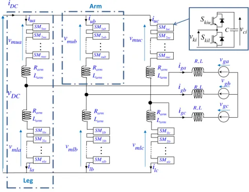
High Voltage Direct Current (HVDC) transmission based on underground cables (or submarines for offshore applications) is an alternative and attractive solution to High-Voltage Alternating Current (HVAC) transmission for long distance. This type of technology is a more and more chosen solution to introduce additionals links in the transmission grid (eg. INELFE between France and Spain [1]). It can also be used for connection of offshore wind farms located far into the see. However, HVDC to HVAC static converters are required for the interconnection with the AC transmission grid. A technological breakthrough in transistor converters has been necessary to cope with the constraints of transmission system, a new structure called Modular Multilevel Converter (MMC) has been proposed [2]. This structure is presented in Fig.1. It is composed of six
arms, each of them composed of elementary sub-modules (SM). These sub-modules consist of a switching cell and a capacitor.
Figure 1. Structural scheme of the MMC.
The MMC structure has many advantages such as its modularity, the absence of high voltage DC capacitor and a very low switching frequency for the transistors. It also has drawbacks such as the complexity to control it due to the large number of semiconductors [1] - [5].
If the realization of a MMC converter exists in academic laboratory, only a dozen converters are referenced in the literature. Apart one very low power converter (800W) operating with 40 SM per arm [6], the other prototypes have only a very low number of SM (2 to 8) [7] to [10]. This type of prototype requires a Pulse Width Modulation (PWM) control and thus generates a high switching frequency which is not really representative of an MMC converter for the HVDC but rather valid for electrical
ga v ga i ua i mua v 1ua SM 2ua SM nua SM mla v 1la SM 2la SM nla SM la i gb v gb i gc v gc i DC i 1ub SM 2ub SM nub SM mlb v 1lb SM 2lb SM nlb SM uc i muc v 1uc SM 2uc SM nuc SM mlc v 1lc SM 2lc SM nlc SM lb i lc i DC v C vci kiu S kil S ki v , R L , R L , R L arm arm R L mub v ub i arm arm R L arm arm R L arm arm R L arm arm R L arm arm R L Leg Arm
machine adjustable speed drives applications [10] - [11]. Moreover, some of them are designed with a non-negligible capacitor on the DC bus.
Given the relatively small number of SMs, all of these prototypes are controlled by a single central control system. This control architecture is feasible with these prototypes since they only require a relatively small number of inputs and outputs. In the full-scale system, this architecture is not suitable since the system must manage more than 2,400 inputs and 2,400 outputs for a 400-level MMC. These prototypes have been sized and proposed to validate the feasibility, converter control, balancing control, thermal operation. They were not sized on the basis of a per-unit approach based on data from existing devices.
This paper aims to present the design of a laboratory MMC prototype with a large number of SM and its control system. The chosen design method is based on the per-unit approach as much as possible with full-scale parameters coming from a 640kV-1GW converter. A control hardware integrating distributed processors (one for each arm) and a master control is presented. The second part proposed a rigorous methodology, based on real time simulation, to test the control algorithm implemented in the different processors which drive the whole converter. The last part of this paper is focused on the test and validation of the sub-modules and the arms of the MMC. A conclusion with perspectives will end the paper.
II. Design of the power part of the converter
The MMC prototype must be as realistic as possible to a full scale MMC, with a large number of SM (i.e. 640kV on the DC side, a rated power of 1GW and 400 sub-modules). The parameters used for the Per-Unit Approach are summarized in the following table I. The values of these parameters come from a realistic value close to the values used for the INELFE link [1].
Table 1. MMC parameters.
Larm 50 mH C 10 mF
Rarm 50 mΩ N 400
L 60 mH VDC 640 kV
R 60 mΩ ω 314 rad.s-1
VCi_ (mean values) 1.6 kV Vg(rms value) 192 kV
P 1GW Q 300 MVAR
2.1 Voltage and power levels
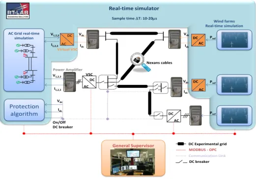
The MMC has been sized adequately to interface it with an existing DC demonstrator [12]. This demonstrator is a 5 terminals DC mesh grid (MTDC) as presented in Fig.2. It consists of a real-time simulation part (blue part) emulating three offshore wind farms and an AC grid and a physical part, which is a low voltage MTDC grid. This physical part is composed by 15 km of low voltage cables DC and two two-level voltage source converter (VSC). The interfacing between the simulated and physical part is done using two AC power amplifiers connected to 2 levels VSCs and three DC power amplifiers.
Figure 2. Scheme of the MTDC mock-up of the Lab. Protection algorithm AC Grid real-time simulation General Supervisor Real-time simulator Wind farms Real-time simulation Power Amplifier Virtual VSC Pref Pref Pref V1,2,3 Idc Vdc Idc I1,2,3 VSC V1,2,3 I1,2,3 DC breaker MODBUS - OPC DC Experimental grid Communication Link Nexans cables Vdc Vdc Idc Vdc Idc On/Off DC breaker Sample time T: 10-20s AC DC AC DC AC DC AC DC AC DC
2 levels VSCs are used firstly in this mockup to validate experimentally the power flows management strategies in the MTDC grid but this technology is not representative of the MMC one which will be probably implemented in MTDC grid.
Replace the two VSC by two MMC prototypes is a good way to improve this Mockup. To do so, the MMC prototypes must withstand a 200V, 50Hz phase to phase voltage and a 400V DC bus voltage. The chosen rated active power is equal to 5 kW and its rated reactive power to 1.5 kVAR.
2.2 Sub-Modules sizing
The choice of the number of Sub Modules (SM) by arm and their design are the most important elements for the prototype design. The choice is a compromise between the following parameters:
This number should be relatively high to ensure a similar behavior to an MMC converter without requiring a PWM control.
The maximum number of SM by arm should consider the following technical constraints:
(1) The minimum acceptable voltage level in the SM.
(2) The Number of I/O available in conventional control device and the architecture of the control
These constraints lead to 20 sub-modules in each arm to design prototypes of MMC.
As presented in [4] and [5], the sum of all the voltages of each SM in an arm is usually close to the DC bus voltage of the converter, 400V for this application. This voltage has to be split equitably on all the SM in the same arm so the nominal chosen
voltage of the SM capacitor (Vcj) is equal to 20V. The maximum voltage of the SM
capacitor is set equal to 30V to allow some margins during operation.
The value of the SM capacitor is determined from the MMC equivalent static inertia. This electrostatic inertia, named HC, is given in equation (1). This HC factor is
around 33ms for a high power converter. To keep this electrostatic inertia value, the SM capacitance should be equal to 8mF.
6 0.5 DC² C C V N H P (1)
For a conventional MMC control as presented in [5] and neglecting the losses in the converter, it is possible to determine, by a power balance, the equation of the instantaneous currents in the upper and lower arm as shown by equation (2). It is used to define the RMS and maximum current value in the sub-modules to choose the semiconductors. ² ² (t) 2 cos( ) 3 6 ² ² ( ) 2 cos( ) 3 6 u a DC g l a DC g P Q P i t V V P Q P i t t V V (2)
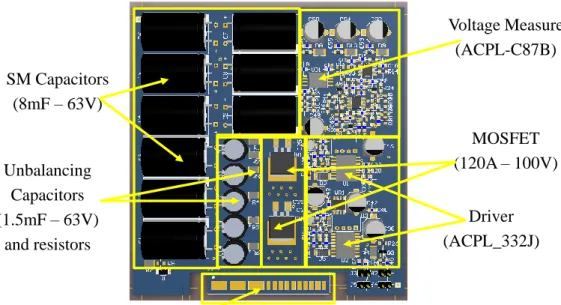
For the desired converter characteristics, these currents are equal to 8,6A RMS and 14,8A for the maximum value. With the voltage and the current levels, the MOSFET PSMN3R8-100BS semiconductors have been chosen to perform the SM switching cell controlled by an ACPL 332J Driver. Fig. 3 shows the result of the design of a sub module. The three arms have an equal sizing. In order to be able to test the robustness of the control, some capacitors and resistances associated with a connector
have been added to the SM to emulate an unbalance between the sub-modules and the arm.
Figure 3. Sub Module board.
2.3 Inductances L and Larm sizing
In high power application, the MMC converter has a large number of SM, the generated voltages have a really good quality (401 levels for the real device), and the inductances are not sized to limit the ripple currents contrary to the classical 2 level VSC but to limit the gradient of the DC and AC currents of the converter in case of a failure of the DC or the AC grid. This sizing is given by equations (3) and (4) respectively for the arm and grid side inductances. Derivative terms are equals to 6.4MA per seconds in the full scale converter [5].
2 DC DC DC R arm di V dt I L (3) max 2 AC AC R grid arm di U dt I L L (4) SM Capacitors (8mF – 63V) Unbalancing Capacitors (1.5mF – 63V) and resistors MOSFET (120A – 100V) Driver (ACPL_332J) Voltage Measure (ACPL-C87B)
The values obtained by this calculation are 4mH for arms inductances and 3.6mH for AC side inductors. In order to have a safety margin and simplify the design of these inductances, the final value is chosen at 5mH for AC the inductors. To limit the DC side current ripple due to the reduction of the number of SM, the arm inductors had to be increased to 10mH.
III. Structure of the control part
Given the number of SM (120 sub-modules for the prototype), a centralized control in a single processor is only possible with an FPGA component. But it has the disadvantage of requiring a larger development time than a classical DSP. In addition, programming a DSP may be accelerated by the rapid prototyping tools.
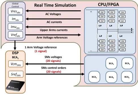
In the development of this prototype, a distributed control structure has been preferred. In the proposed architecture (Fig. 4), the control part is divided between a master DSP and six slaves DSP. Each slave provides close control (switching function generation and SM arms control balancing algorithm (CBA)) of each arm while the Master provides the global control with slower dynamic (control the power and the stored energy into the MMC). The master ensures also the communication with the SCADA system. The communication between the master and slaves DSP is done by optical links where informations are exchanged at 100kHz. Three dedicated lines are used by each slave: one for synchronization, one for inputs and one for outputs. each DSP slave provides to the master one the sum of the capacitor voltage of its arm while the master transmits, to each slave, its reference of voltage that the associated arm must generate.
Figure 4. Architecture of the control.
The chosen slaves DSP are the Texas TMS320F28377D as they have enough analog input (24 in total). The same reference has been selected for the master DSP for implementation simplicity. The selected slave DSPs have 16 outputs configurable in PWM mode or not. These outputs have been used to control 16 SM without activating the PWM mode. It is quite possible to reduce the number of SM in the prototype and activate the PWM mode.
IV. Validation methodology and experimental results
4.1 Validation of the control
To test the control algorithms while minimizing the risk of material destruction, control algorithms have been validated with Hardware in the Loop (HIL) tests. Firstly, a detailed model equivalent in real time to our MMC prototype is of highest importance. This model, presented in Fig. 5, is based on the real-time model developed in [13] and implemented on an Opal RT system. It is split on two parts: one on a CPU, the other
part on a FPGA. The results obtained with the real-time simulation will be considered as the reference results. The idea in the sequel is to include control hardware in the real-time environment to test the actual control algorithm in a highly realistic situation.
Figure 5. Scheme of the detailed equivalent model in real-time simulator. [13]
4.1.1 Validation of the slave control
The CBA implemented on each slaves DSP is the Reduced switching-frequency voltage-balancing algorithm presented in [14]. To test the implemented control in the slave DSP, a CBA algorithm was removed from the Real Time simulation as shown in Fig. 6. This control was replaced by a real slave DSP and interfaced via its input/output to the Real Time simulation. The global control set in the real-time simulation is a classical energy based control as presented in [4]. Fig. 7 shows the experimental bench to validate the control implemented in the slave DSP. Fig. 8 shows SM voltages of one arm with a full simulation (a) and a simulation associated with a slave DSP (b).
AC Grid
Data acquisition synchronized on CPU time step
CPU Time step : 30-15µs Execution time for models and nodal solution (4-15µs) Data processing with IOs CPU MMC Arm model Signals to CPU: 6 Rn, 6In, 120 Capacitor Voltages
Signals from CPU: 6 arm currents Time step
<2µs
PCI-E communication bus
CPU FPGA Control system model CPU Converter model Rn1 In1 Rn2 In2 Rn3 In3 Rn4 In4 Rn5 In5 Rn6 In6 Direct communication with FPGA or communication through PCI-E bus
Figure 6. Scheme of the detailed equivalent model in real-time.
Fig 7. Picture of the HIL test bench of the balancing algorithm
SM SM SM SM SM SM SM SM SM SM SM SM SM SM SM SM SM SM BCA5 BCA6 BCA3 BCA4 BCA2 CPU/FPGA Real Time Simulation
DSP
BCA1
Arm Voltage references
Imabc Imuabc Vresabc Vrefabc AC Voltages AC currents Upper Arms currents
SrefSMs VcmSMs SMs control orders (20 signals) SMs voltages (20 signals)
1 Arm Voltage reference
(1 signal)
Global Control
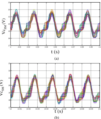
Figure 8. Voltages of the 20 SM in test with the real-time simulator (a), with the balancing algorithm in the external DSP (b).
It can be concluded from these results that the balancing control implemented in the DSP performed correctly its balancing control. The SMs voltages are properly balanced and the variation is similar. The difference is explained by the generated measurement noise during the signals acquisition in the DSP.
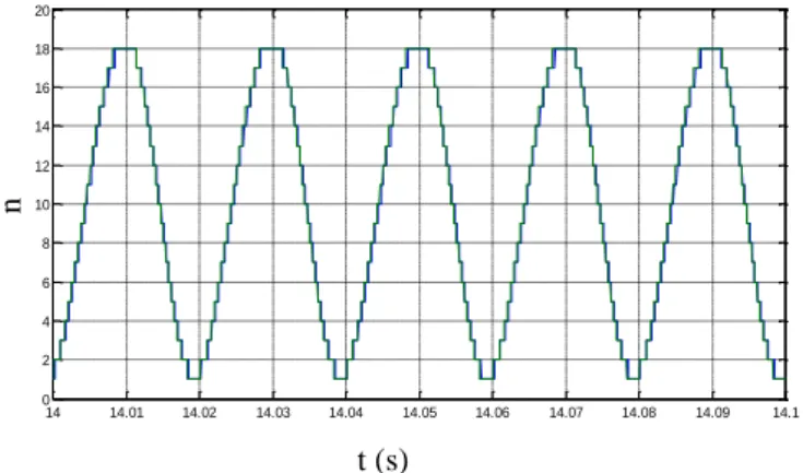
Fig. 9 shows the reference tracking by a comparison between the number of activated SM (n) by a complete real-time simulation and a simulation associated to a slave DSP. 4 4.01 4.02 4.03 4.04 4.05 4.06 4.07 4.08 4.09 4.1 17 18 19 20 21 22 23 14 14.01 14.02 14.03 14.04 14.05 14.06 14.07 14.08 14.09 14.1 17 18 19 20 21 22 23 Vc SM (V) Vc SM (V) t (s) t (s) (a) (b)
Figure 9. Comparison between the numbers of activated SM: with DSP in green and real time simulation in blue.
It is possible to conclude from this result that the control developed in the DSP performs properly its reference tracking task even if a slight difference has been noticed between the full real-time simulation and when the actual DSP is interacting with the real-time simulation
4.1.2 Validation of the master control
After testing the DSP dedicated to BCA, the global control implemented in the master DSP is also tested in the real-time environment (Fig. 10). It has been interfaced with its input/output to the simulation Real Time.
14 14.01 14.02 14.03 14.04 14.05 14.06 14.07 14.08 14.09 14.1 0 2 4 6 8 10 12 14 16 18 20 t (s) n
Figure 10. HIL scheme for the validation of the global control.
Fig. 11 shows the comparison between the results with the full simulated (in red) and with the DSP (blue) for id grid current, the DC current and the differential current of
an arm current of MMC. The difference is mainly explained by the effect of sampling. The control is done by classical PI controllers with a time response set at 5ms for all current loops and 10ms for all voltage loops with a ζ equal to 0,7. The MMC is controlled as presented in [3] and [4].
Arm voltage references
(6 signals) BCA5 BCA6 BCA3 BCA4 BCA1 BCA2 Global control Igabc Iuabc Vgabc Vmlabc_ref Vmuabc_ref AC Voltage (ph-ph) (2 signals) AC currents (3 signals)
Upper Arms currents
(3 signals) SM SM SM SM SM SM SM SM SM SM SM SM SM SM SM SM SM SM
Figure 11. Current controls results for id grid current (a), the DC current (b) and the
differential current of an arm current (c). Full real-time simulation (in red) , global control implemented in the DSP (in blue)
Fig. 12 shows the results between vctot voltages of a MMC arm for a global
control fully simulated (a) and the global control into the DSP (b). In steady state, the voltages are similar. Some slight differences are noticed during the transient. The upper voltage of the presented arm appears in red when the lower one appears in blue. The
16.2 16.3 16.4 16.5 16.6 16.7 -5 0 5 10 15 20 id (A ) t (s) 16.2 16.3 16.4 16.5 16.6 16.7 -5 0 5 10 15 20 25 iDC (A ) t (s) 16.2 16.3 16.4 16.5 16.6 16.7 -2 0 2 4 6 8 10 t (s) idiff (A ) (a) (b) (c)
currents in the AC grid are generated at 50% by the upper arm and 50% by the lower one, a phase shift of 180º arise between the vctot voltages of a MMC arm
Figure 12. vctot voltages of a MMC arm for a global control full real-time simulation (a)
or when the global control is implemented in the DSP (b).
4.2 Validation of the power stage
4.2.1 Validation of sub-modules
A sub-module (SM) has a similar operation as a boost chopper except that, in the case of the MMC operation, the arm current flows through the capacitor when the SM is activated as shown in Fig. 13.
16.4 16.45 16.5 16.55 16.6 16.65 16.7 16.75 16.8 320 340 360 380 400 420 440 460 16.4 16.45 16.5 16.55 16.6 16.65 16.7 16.75 16.8 320 340 360 380 400 420 440 460 t (s) t (s) Vc tot (V) Vc tot (V) (a) (b)
Figure 13. Principle of the SM operation.
Therefore the validation of the SM requires a particular electrical circuit which
allows to test the different configurations of the SM
avoids to charge or discharge the capacitor.
The mean value of the current in the capacitor must be equal to zero. Fig. 14 shows the proposed electrical scheme to make it possible these two previous conditions.
Figure 14. Proposed test setup.
Source 1 is a voltage source. The switching frequency on the SM can be set from 400 to 1000 Hz. Source 2 is synchronized with this switching signals applied. Depending on the state of SM, it can act as a voltage source or current source.
T1= 0 et T2= 1 T1= 1 et T2= 0 T1 T2 D1 D2 T2 D2 D1 T1 ISM IC VSM ISM ICH T2 D1 Source 2 Source 1 VC VT2 D2 T1
Fig. 15 shows the two operating states of the proposed setup.
SM activated (Fig. 15a), the current in the inductance decreases. Ic = Ism. Source 2 is a current source: ICH= 0A
SM By-passed (Fig. 15b), the current in the inductance increases. Source 2 is a voltage source. The voltage is set to 19V in order to discharge of the capacitor.
The duty cycle controls the average value of VT2 so the average value of the
current in the SM.
Figure 15. The two operating states of the proposed setup.
Fig. 16 shows the results obtained from this operating mode for a switching frequency equal to 400 Hz, an average operating voltage equals to 20 V and with 10A of average current. From these results, it is possible to observe the control signal (blue curve), the voltage of the storage element (the green curve), the current of the sub-module (brown curve) and the current of the Programmable load (yellow curve). These results show the two operating mode of the sub-module (activated mode and by-pass mode). With these two phases, the voltage of the sub-module varies between the minimum and maximum limit values as the operating mode of a sub-module in a complete MMC.
Figure 16. Electrical waveform of the SM during the test.
Thanks to this set up, it was possible to check the dynamic behavior of the sub module and also the thermal behavior (Fig. 17). The temperature does not exceed 45°C. All These tests validate the design of the sub-module.
Figure 17. Validation of the SM behavior with the thermal camera.
D1 T2 I C VT2 ISM VC ICH ICH VT2 VC ISM By Pass Activate
4.2.2 Validation of the arm
Fig. 18 shows the design of one arm composed by the twenty sub-modules.
Figure 18. Photo of one arm composed of 20 sub modules.
Fig. 19 shows the scheme to validate the whole arms. The aim is to test the behavior of the arm when the nominal current is circulating. To do so, a DC and AC source is used and generated by a chopper. The R-L impedance between the arm and the voltage source is the arm inductance. The modulated voltage (Vm) is controlled by the
state of the sub-modules. In a first step, Vm equals to V: the current is null. A phase shift
is then applied to the sinusoidal component of Vm to generate a current in the arm.
The control of the arm is done in open loop since the control of the currents and the stored energy is done by the master DSP in the laboratory MMC previously validated.
Figure 19. Principle of validation of arms.
Fig 20 shows the result of the first tests of the arm, with a zero phase shift thus no current is generated in the system. We can see, in violet, the waveform of the arm voltage generated by the arm which is in the stair case waveform with 21 levels.
Figure 20. Modulated voltage of the arm Vm (blue) and the output voltages of the
chopper (in violet) for zero phase shift. L
R
Vdc/2
Vs
Fig. 21 shows results of a similar test but with a non-zero phase shift. The amplitude of the current is equal to the desired amplitude. The perturbed waveform of this current is easily explained since the system operates in open loop.
Figure 20. Modulated voltage of the arm Vm (blue) and the arm current (in green) for
not zero phase shift. The temperature of each arm does not exceed 52°C at the rated power.
V. Conclusion
This article presents the sizing method of a laboratory Modular Multilevel Converter with 20 SM and its control architecture. The chosen design method is based on a per-unit approach with data from a 1GW, 640kV. A control architecture, constrained by the number of sub-modules, is presented. The protocols for testing and validating the sub-modules, the arms and then all controls have been presented. These validated elements are the basic elements for the realization of the MMC laboratory prototypes. The assembly, in a bay, of the six arms with the control device cards is the last step to produce the MMC converter. The MMC prototype is therefore in its final stage.
VI. References
[1] Saad H, Dennetiere S, Mahseredjian J, et al. Detailed and Averaged Models for a 401-Level MMC– HVDC System, IEEE Trans. Power Delivery, Vol. 27 no 3, July 2012, pp. 1501-1508.
[2] Marquardt R, Lesnicar A, A new modular voltage source inverter topology, Proceeding of the 10th European Conference on Power Electronics and Application, EPE, 2003 Sept 2-4, Toulouse, France; 2003. [3] Delarue P, Gruson F, Guillaud X, Energetic Macroscopic Representation and Inversion Based Control of a Modular Multilevel Converter, European Conference on Power Electronics and Application, 2013 European Conference on Power Electronics and Applications (EPE'13 ECCE-Europe), 2013 Sept 3-5, Lille, France; 2013.
[4] F. Gruson, J. Freytes, S. Samimi, P. Delarue, X. Guillaud, F. Colas, M.M. Belhaouane, "Impact of control algorithm solutions on Modular Multilevel Converters electrical waveforms and losses," 2015 17th European Conference on Power Electronics and Applications (EPE'15 ECCE-Europe), Geneva, 2015, pp. 1-10.
[5] Samimi S, Gruson F, Delarue P, et al. Energetic Macroscopic Representation and PQ diagram of modular multilevel converter, symposium de genie electrique SGE, 2014 july8-10, Cachan, France, in French.
[6] Zhou Y, Jiang D, Hu P, et al., A Prototype of Modular Multilevel Converters, in IEEE Trans on Power Electronics, vol.29, no.7, pp.3267-3278, July 2014.
[7] Darus R, Pou J, Konstantinou G, et al., A modified voltage balancing sorting algorithm for the modular multilevel converter: Evaluation for staircase and phase-disposition PWM, 2014 IEEE Applied Power Electronics Conference and Exposition - APEC 2014, Fort Worth, TX, 2014, pp. 255-260.
[8] Vasiladiotis M, Cherix N, Rufer A, Accurate Capacitor Voltage Ripple Estimation and Current Control Considerations for Grid-Connected Modular Multilevel Converters, IEEE Trans Power Electronics, vol. 29, no. 9, pp. 4568-4579, Sept. 2014.
[9] Wu C. M. Etude prospective de la topologie MMC et du packaging 3D pour la réalisation d'un variateur de vitesse en moyenne tension [dissertation]. Université Grenoble Alpes; 2015, in French.
[10] Clemow P, Judge P, Chaffey G, et al. M, Lab-scale experimental multilevel modular HVDC converter with temperature controlled cells European Conference on Power Electronics and Application, EPE’14 ECCE Europe, 2014 aug. 26-28, Lappeenranta, Finland, 2014.
[11] Serbia N, Modular Multilevel Converters for HVDC power stations [PhD dissertation]. Institut National Polytechnique de Toulouse - INPT, 2014.
[12] S. A. Amamra; F. Colas; X. Guillaud; P. Rault; S. Nguefeu, "Laboratory Demonstration of a Multi-Terminal VSC-HVDC Power Grid," in IEEE Trans. Power Delivery, vol.PP, no.99, pp.1-1
[13] Ould-Bachir T; Saad H; Dennetiere S, et al., "CPU/FPGA-based Real-Time Simulation of a Two-Terminal MMC-HVDC System," in IEEE Trans. Power Delivery, vol.PP, no.99, pp.1-1
[14] Qingrui Tu, Zheng Xu and Lie Xu, "Reduced switching-frequency modulation and circulating current suppression for modular multilevel converters," PES T&D 2012, Orlando, FL, 2012, pp. 1-1.

![Figure 5. Scheme of the detailed equivalent model in real-time simulator. [13]](https://thumb-eu.123doks.com/thumbv2/123doknet/7348355.212823/12.892.129.431.234.632/figure-scheme-detailed-equivalent-model-real-time-simulator.webp)