HAL Id: tel-01698990
https://pastel.archives-ouvertes.fr/tel-01698990
Submitted on 1 Feb 2018HAL is a multi-disciplinary open access archive for the deposit and dissemination of sci-entific research documents, whether they are pub-lished or not. The documents may come from teaching and research institutions in France or abroad, or from public or private research centers.
L’archive ouverte pluridisciplinaire HAL, est destinée au dépôt et à la diffusion de documents scientifiques de niveau recherche, publiés ou non, émanant des établissements d’enseignement et de recherche français ou étrangers, des laboratoires publics ou privés.
grown by atomic layer deposition for low temperature
solar cells processes
Fabien Lebreton
To cite this version:
Fabien Lebreton. Silicon surface passivation properties of aluminum oxide grown by atomic layer deposition for low temperature solar cells processes. Material chemistry. Université Paris Saclay (COmUE), 2017. English. �NNT : 2017SACLX109�. �tel-01698990�
NNT : 2017SACLX109
T
HESE DE DOCTORAT
DE
L’U
NIVERSITE
P
ARIS
-S
ACLAY
PREPAREE A
L’ECOLE
POLYTECHNIQUE
E
COLED
OCTORALE N°573 : interfaces
Approches interdisciplinaires : fondements, applications et innovation
Spécialité : Chimie des matériaux
Par
M. Fabien Lebreton
Silicon surface passivation properties of aluminium oxide
grown by atomic layer deposition for low temperature solar cells processes
Thèse présentée et soutenue à Palaiseau, le 20 décembre 2017 :
Composition du Jury :
Dr. Kleider, Jean-Paul GeePs Président du jury
Prof. Glunz, Stefan Fraunhofer ISE Rapporteur
Dr. Blanc-Pelissier, Danièle INL Rapporteur
Dr. Broussillou, Cédric EDF Examinateur
Dr. Betremieux, Isabelle TOTAL Examinatrice
Dr. Filonovich, Sergej TOTAL Encadrant
“Discovery consists of seeing what everybody else has seen, and thinking what nobody else has thought.”
Albert Szent-Gyorgyi
Remerciements
Ces trois courtes et intenses années de thèse se sont déroulées entre Total et le Laboratoire de Physique des Interfaces et Couches Minces (LPICM) via une convention CIFRE. Je tiens donc à remercier en premier lieu Fabrice Devaux et Lars Oberbeck pour m’avoir permis d’intégrer l’équipe R&D de Total, mais également, Pere Roca i Cabarrocas pour m’avoir ouvert son laboratoire et fait bénéficier de son expertise sur tous les pans de ce que peut être la Recherche.
Il est important pour moi de témoigner ma sincère gratitude à François Silva qui fut un directeur de thèse hors pair. Ses conseils avisés, sa disponibilité, son soutien et son exceptionnelle capacité à voir la tasse de Nespresso à moitié pleine ont été d’une grande aide tout au long de ces trois années. En ce sens, je suis également reconnaissant envers Sergej Filonovich de m’avoir épaulé au sein de Total et d’avoir su garder le sens de l’humour en toutes circonstances.
Par ailleurs, pour l’honneur qu’ils m’ont fait en acceptant de siéger au jury de cette thèse je remercie, Isabelle Betremieux, Danièle -BlancPelissier, Cédric Broussillou, Stefan Glunz et
Jean-Paul Kleider.
Mes travaux ayant été principalement rattachés aux projets de l’Institut Photovoltaïque d’Ile de France (IPVF), je souhaite en remercier les membres avec lesquels j’ai eu l’opportunité de collaborer : Thomas Blévin, Coralie Charpentier, François Cœuret, Jean-Yves Letellier, Yves
Marot, Sylvain Pouliquen et Andy Zauner côté Air Liquide ; Philippe Baranek, Julien Couderc, Julien Dupuis, Pierre-Philippe Grand et Vanessa Riffet côté EDF.
Ce travail doctoral n’aurait pu être mené à bien sans les discussions, la disponibilité et la collaboration de nombreux collègues du laboratoire. Je remercie donc chaleureusement, Pavel
Bulkin (une ligne pilote à lui seul), Wanghua Chen, Dmitri Daineka, Alice Defresne, Ileana Florea, Martin Foldyna, Enric Garcia-Caurel, Erik Johnson (pour m’avoir fait découvrir les
réalisateurs originaires de Winnipeg entre 1972 et 1973), Rasha Khoury, Jean-Luc Maurice,
Jean-Luc Moncel, Karim Ouaras, Denis Tondelier, Jacqueline Tran, Sandrine Tusseau-Nenez, Junkang Wang. Merci également à l’équipe administrative ; Laurence Corbel, Gabriela Medina
et Fabienne Pandolfe. De plus, je ne saurais oublier ceux qui maintiennent notre environnement en état et réparent quand une pompe primaire brûle ou quand un ordinateur crashe, c’est-à-dire l’équipe du BEER & WINE : Nacib Benmammar (♪ mets de l'huile petit homme dans la vie il faut que ça pompe ♪), Jérôme Charliac, Frédéric Farci, Cyril Jadaud, Frédéric Liège et Eric
Paillassa et Jean-Charles Vanel.
Mes remerciements vont également à l’équipe de Total qui animait la vie de l’annexe du 404 à Palaiseau, à savoir Ahmed Ben Slimane, Jean-François Besnier, Amjad Deyine, Jara
Fernandez, Nada Habka, Ludovic Hudanski, Vincent Maillard, Julien Penaud (de temps à
autres), Gilles Poulain, Patricia Prod’homme, Céline Richard, et Martin Sander . Je n’oublie pas les Belges régulièrement de passage : Guillaume Courtois et Patricia De Coux.
Je souhaite remercier de tout cœur ceux qui ont marqué ma vie quotidienne au long de ces trois années, notamment l’équipe des doctorants et assimilés : Linda Assam, Bastien Bruneau,
Romain Cariou, Marta Chrostowski, Jean-Christophe Dornstetter (startupper dans l’âme), Etienne Drahi (super collaborateur mais surtout guide touristique à toutes heures), Gwenaëlle Hamon (véritable athlète-orchestre), Ronan Léal (la relève des 3x8), Amadéo Michaud, Paul Narchi (heureux de voir que tu n’as pas persisté dans l’humour), Rafaël Peyronnet, Igor Sobkowicz, Nicolas Vaissière (l’homme providentiel). Une mention toute particulière à Guillaume Fischer, éternel cobureau, pour nos nombreux échanges scientifiques mais surtout
pour tous ceux qui ne l’étaient pas.
Aux collègues de passages, Emmanuel Courtade, Clément Lausecker, et qui parfois s’installent tels que Katia Allaoua (bravo pour le marathon des innombrables caractérisations) et
Mengkoing Sreng : un grand merci.
Je tiens également à remercier les collègues des autres laboratoires avec lesquels j’ai eu le plaisir de travailler : Cyril Bachelet et Nicolas Pauwels (pour m’avoir initié aux analyses par faisceaux d’ions) ainsi que Olivier Plantevin du CSNSM ; Arnaud Devos et Patrick Emery de Menapic pour leur son et lumière très instructif ; José Alvarez (pour son expertise sur mes travaux) mais aussi Raphaël Lachaume du GeePS à qui je dois la concrétisation des sujets qui me trottaient en tête depuis longtemps.
« Большое спасибо» à Sergey Abolmasov, Aleksei Abramov et Ilya Nyapshaev de « TF-TE Ioffe R&D center » pour m’avoir ouvert leur laboratoire mais surtout pour m’avoir fait découvrir la culture Russe au travers de ce qu’elle a de plus authentique. Cette expérience restera l’une des plus enrichissantes de ces trois dernières années.
Pour finir, je remercie mes proches, famille et amis, pour leur soutien. Un merci tout particulier à Stéphanie pour sa patience, ses encouragements et pour avoir compris les concessions inhérentes à la réalisation de ce travail.
Contents
INTRODUCTION... 1
SOLAR ENERGY OUTLOOK ... 1
THESIS AIM AND OUTLINE ... 3
1 THEORETICAL AND EXPERIMENTAL CONTEXT ... 5
1.1 SOLAR CELLS PHYSICS... 6
1.1.1 Device performance ... 6
1.1.2 Recombination ... 7
1.1.3 Passivation ... 8
1.1.4 The effective lifetime of minority carriers ... 10
1.2 CHARACTERISATION TECHNIQUES ... 12
1.2.1 Electrical properties ... 12
1.2.1.1 Photoconductance decay ... 12
1.2.1.2 PCD calibrated photoluminescence mapping ... 13
1.2.1.3 Corona Oxide Characterisation Of Semiconductor ... 13
1.2.2 Optical properties ... 14
1.2.2.1 Spectroscopic ellipsometry ... 14
1.2.2.2 Spectrophotometry ... 15
1.2.3 Material properties ... 16
1.2.3.1 X-ray Reflectometry ... 16
1.2.3.2 Ion beam analysis technique... 18
1.2.3.3 Thermal Desorption Spectroscopy ... 18
1.2.3.4 Vibrational spectroscopy ... 18
2 AL2O3 DEPOSITION AND BASIC PROPERTIES ... 19
2.1 STATE OF THE ART OF ATOMIC LAYER DEPOSITION OF ALUMINIUM OXIDE ... 20
2.1.1 Atomic Layer Deposition ... 20
2.1.1.1 Concept ... 20
2.1.1.2 Importance of the initial surface ... 21
2.1.1.3 Process definition ... 22 2.1.2 Material properties ... 23 2.1.3 Passivation properties of Al2O3 ... 27 2.1.3.1 Substrate specifications ... 27 2.1.3.2 Chemical passivation ... 30 2.1.3.3 Electrostatic passivation ... 32
2.2 LIGHT INDUCED FIELD EFFECT ENHANCEMENT... 33
2.2.1 A well-known fact ... 33
2.2.2 Detailed study of LIFE2 ... 36
2.2.2.1 Monofacial vs bifacial effect ... 36
2.2.2.2 Low intensity bifacial illuminator (LIBI) ... 39
2.2.2.3 Impact of the wavelength ... 42
2.2.2.4 The crucial role of post deposition annealing ... 45
2.2.2.5 Electron trapping in Al2O3 ... 48
3 LIGHT INDUCED FIELD EFFECT ENHANCEMENT OF AL2O3/A-SINX:H STACKS ... 51
3.1 THE A-SINX:H FILM ... 52
3.1.1 The necessity of a capping layer ... 52
3.1.1.1 Optical requirements... 52
3.1.1.2 Stability requirement... 52
3.1.1.3 Passivation requirement ... 53
3.1.1.4 Metallisation constraint ... 53
3.1.2 Plasma-Enhanced Chemical Vapour Deposition ... 53
3.1.3 a-SiNX:H properties ... 55
3.2 IMPACT OF CAPPED AL2O3 PARAMETERS ON LIFE2 ... 62
3.2.1 Process flow ... 62
3.2.2 Expected passivation trends ... 63
3.2.1 Passivation study ... 63
3.3 CONCLUSION ... 68
4 BLISTERING: WITNESS OF THE AL2O3/C-SI INTERFACE DEGRADATION ... 69
4.1 BLISTERING ... 70
4.1.1 Overview ... 70
4.1.2 Gas release ... 72
4.1.3 Blistering statistics ... 74
4.1.4 Al2O3/c-Si interface analysis by coloured picosecond acoustics microscopy ... 78
4.2 HYDROGEN MANAGEMENT DURING ALD ... 83
4.2.1 Concept of the Thermal Drift Atomic Layer Deposition... 83
4.2.1.1 Current strategies to avoid blistering ... 83
4.2.1.2 TD-ALD process simulation ... 83
4.2.2 Standalone TD-ALD Al2O3 ... 85
4.2.3 TD-ALD for Al2O3/a-SiNX:H passivation stacks ... 89
4.3 CONCLUSION ... 91
5 INTERACTION BETWEEN AL2O3 AND ITS A-SINX:H CAPPING LAYER ... 93
5.1 LIFE2 INSTABILITY FOR THIN AL2O3 ... 94
5.1.1.1 Electrostatic in a-SiNX:H... 94
5.1.2 Simulation of the electrostatic shading ... 97
5.2 OPTIMISATION OF THE ELECTROSTATIC STACKING ... 100
5.2.1 Alternative case #1: the SiO2 buffer layer ... 100
5.2.1.1 Experimental environment ... 100
5.2.1.2 Synthesis of the buffer layer ... 101
5.2.1.3 Insertion of the buffer layer in the stack ... 102
5.2.2 Alternative case #2: a-SiNX:H capping replacement ... 104
5.2.2.1 Approach and specification of the desired a-SiNX:H ... 104
5.2.2.2 Synthesis of the new a-SiNX:H capping ... 105
5.2.2.3 Performances of the new a-SiNX:H capping ... 110
5.3 CONCLUSION ... 113
CONCLUSION AND PERSPECTIVES ... 113
CHEMICAL PASSIVATION:DIT REDUCTION ... 115
FIELD EFFECT PASSIVATION:QF INCREASE ... 116
List of Figures
FIGURE 0.1:NUMBER OF PEOPLE WITHOUT ACCESS TO ELECTRICITY OR TO PROPER COOKING FACILITIES AROUND THE WORLD [13].DATA ARE REPORTED ON THE WORLD SOLAR RESOURCE MAP (GLOBAL HORIZONTAL IRRADIATION)[36]. ... 1 FIGURE 0.2:(A)PRICE OF THE C-SI PHOTOVOLTAIC CELLS (LEFT AXIS) AND WORLD INSTALLED PV CAPACITY (RIGHT AXIS)[32,33].(B) MARKET
SHARE FORECASTS FOR THE MAIN SOLAR CELLS ARCHITECTURES AND PROPORTION OF BIFACIAL SOLAR MODULES [38]. ... 2 FIGURE 0.3:(A)BAND STRUCTURE OF AL-BSF WHERE VB STANDS FOR VALENCE BAND AND CB FOR CONDUCTION BAND (B)SCHEMATIC CROSS
SECTION OF AL-BSF AND PERC SOLAR CELLS. ... 2 FIGURE 1.1:SCHEMATIC REPRESENTATION OF (A) RADIATIVE RECOMBINATION;(B)AUGER RECOMBINATION INVOLVING EEH (C) EHH;(D)SRH
RECOMBINATION AND (E) SURFACE RECOMBINATION... 7 FIGURE 1.2:BAND ALIGNMENT BETWEEN C-SI AND SIO2.THE YELLOW AREA CORRESPONDS TO THE BANDGAP BETWEEN THE VALENCE BAND
MAXIMUM (VBM) AND THE CONDUCTION BAND MINIMUM (CBM).THE ZERO OF ENERGY IS CHOSEN AT THE VBM OF SIO2.
CALCULATED LEVELS FOR VARIOUS POINT DEFECTS IN A-SIO2 ARE REPORTED ON THE GRAPH.THE EXPONENT NUMBER IS THE NET
CHARGE OF THE DEFECT.FROM THE LEFT TO THE RIGHT OF THE HORIZONTAL AXIS DEFECTS ARE:SI-SI BONDS;SI DANGLING BONDS (SIDB);SI-H;O DANGLING BONDS (ODB); PEROXYL BRIDGES (O-O); AND THE PLANAR O3+(INDEX MEANS TRIPLY COORDINATED).
ADAPTED FROM [34] ... 9 FIGURE 1.3:ELECTRON AND HOLE DENSITY BELOW THE SI SURFACE FOR (A) P-TYPE AND (B) N-TYPE SI UNDER INFLUENCE OF A NEGATIVE FIXED
SURFACE CHARGE OF QF=2·10
12
CM-2;(C) BAND BENDING UNDER INFLUENCE OF QF.DATA SIMULATED BY PC1D FOR 2 Ω.CM
WAFERS UNDER ILLUMINATION.TAKEN FROM [37]. ... 10 FIGURE 1.4:(A)RECOMBINATION RATE AND (B) EQUIVALENT BULK LIFETIME FOR A C-SI WAFER WITH A DOPANT DENSITY NA OF 4.68·1015CM-3
AT 300 K. ... 11 FIGURE 1.5:EFFECTIVE LIFETIME OF TWO SAMPLES (P-TYPE) PASSIVATED BY AL2O3/A-SINX:H STACKS.SAMPLE #1 HAS A 60 ALD CYCLE THICK
AL2O3 LAYER AND IS A QUARTER OF 100MM WAFER WHILE SAMPLE #2 HAS A 100 ALD CYCLES THICK AL2O3 LAYER AND IS A FULL 100MM WAFER. ... 12 FIGURE 1.6:PCD-CALIBRATED PHOTOLUMINESCENCE MAPPING OF AN INTRINSIC WAFER OF 100MM DIAMETER, PASSIVATED BY 1000 ALD
CYCLES DEPOSITED AT 300 °C.THE PICTURE IS TAKEN FOR A MINORITY CARRIER DENSITY OF 2·1015CM-3. ... 13 FIGURE 1.7:GEOMETRY FOR SE MEASUREMENTS. ... 15 FIGURE 1.8:GEOMETRY FOR XRR MEASUREMENTS.THE DETECTOR SLIT WAS 0.6MM WIDE, OTHER SLITS WERE 0.1MM WIDE, PRIMARY
SOLLER WAS AXIAL (2.5°) WHILE SECONDARY SOLLER WAS EQUATORIAL (0.3°).THE X-RAY SOURCE OPERATED AT A VOLTAGE OF
40KV AND CURRENT 40MA, PRODUCING A MONOCHROMATIC RADIATION OF Λ =1.54 Å(CU KΑ1)... 16
FIGURE 1.9:XRR EXPERIMENTAL DATA (BLACK DOTS) AND FITS (RED LINES) FOR THREE AMORPHOUS MATERIALS DEPOSITED ON C-SI.THE AL2O3 LAYER WAS DEPOSITED BY 200 ALD CYCLES AT 250 °C(CHAPTER 2), THE A-SINX:H LAYER WAS DEPOSITED BY PECVD
(CHAPTER 3) AND THE SIO1.6 WAS ALSO DEPOSITED BY PECVD(CHAPTER 5).FOR REFERENCE, C-SI DENSITY IS 2.33G.CM-3. ... 17
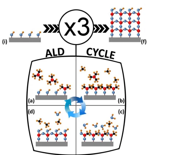
FIGURE 1.10:GEOMETRY FOR RBS(Α=0°; Β=30°) AND ERDA(Α=75°; Β’=75°) MEASUREMENTS.INCIDENT HE+ ENERGY WAS 1.6 MEV, THE MYLAR FOIL THICKNESS WAS 8µM. ... 18 FIGURE 2.1:PRINCIPLE OF ALD PROCESS BASED ON TMA AND H2O.BLUE, YELLOW, RED AND BLACK SPHERES ARE ATOMS OF OXYGEN,
HYDROGEN, ALUMINIUM AND CARBON RESPECTIVELY.AN ALD CYCLE CONSISTS OF (A)TMA PULSE (B)PURGE OF BY-PRODUCTS AND REMAINING TMA(C)H2OPULSE (D) PURGE OF BY-PRODUCTS AND REMAINING H2O.FROM INITIAL SURFACE (I), BY REPEATING
THE ALDCYCLE 3 TIMES (FROM A TO D) THE FINAL SURFACE (F) IS COVERED BY AN ALDFILM OF APPROXIMATELY 3 Å. ... 21 FIGURE 2.2:(A)THICKNESS MAPPING (80 POINTS) OBTAINED BY SE AFTER THE DEPOSITION OF 200 ALD CYCLES ON EACH SIDE.(B)OPENED
SUBSTRATE HOLDER ALLOWING A DOUBLE SIDE DEPOSITION. ... 23 FIGURE 2.3:(A)GROWTH PER CYCLE AS A FUNCTION OF THE DEPOSITION TEMPERATURE.THE STARS FROM YLIVAARA ET AL. ARE THE
REPETITION OF EACH HALF CYCLE 5 TIMES BEFORE SWITCHING TO THE OTHER HALF CYCLE.(B)OXYGEN/ALUMINIUM RATIO (DETERMINED BY RBS) AS A FUNCTION OF THE DEPOSITION TEMPERATURE. ... 23
FIGURE 2.4:(A)FILM DENSITY AS A FUNCTION OF THE DEPOSITION TEMPERATURE.REPORTED VALUES FOR THIS WORK ARE THE AVERAGE DENSITY AS A DENSITY GRADIENT IS NECESSARY TO FIT THE DATA.ERROR BARS ARE THE STANDARD DEVIATION DUE TO THIS
GRADIENT.(B) REFRACTIVE INDEX DETERMINED BY SE AT 633NM USING SELLMEIER DISPERSION LAW. ... 24
FIGURE 2.5:HYDROGEN AND CARBON CONCENTRATION.FOR THIS WORK, HYDROGEN CONTENT HAS BEEN MEASURED BY ERDA WHILE CARBON HAS BEEN QUANTIFIED BY SIMS MEASUREMENTS CALIBRATED THANKS TO NRA. ... 25
FIGURE 2.6:(A) ERDA SPECTRA OF THE 5 SAMPLES DEPOSITED AT DIFFERENT TEMPERATURES.DISCRETE POINTS ARE ACQUIRED DATA AND RED CURVES ARE DATA FITS.(B) EFFECTIVE LIFETIME OF THE AS DEPOSITED SAMPLES WITH 1000 CYCLE AL2O3. ... 26
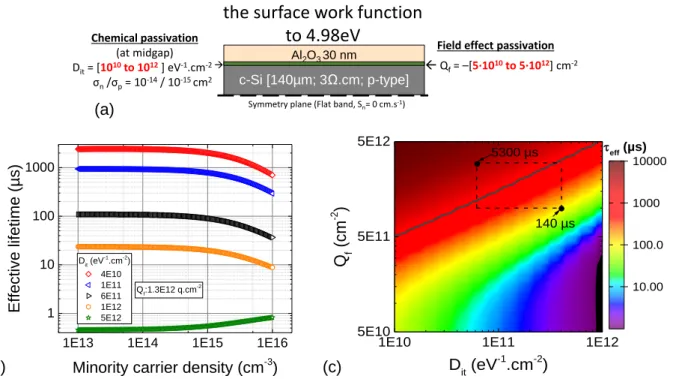
FIGURE 2.7:(A)SIMULATION MODEL USED TO EVALUATE THE MINORITY CARRIER LIFETIME.(B) EFFECTIVE LIFETIME AS A FUNCTION OF THE INJECTION LEVEL FOR ONE VALUE OF QF AND SEVERAL DIT.(C)EFFECTIVE LIFETIME AS A FUNCTION OF QF AND DIT FOR AN INJECTION LEVEL OF 1015CM-3.THE SOLID LINE CORRESPONDS TO THE LIFETIME OF 1300µS (SRV=10CM.S-1) AND DASHED LINES DELIMIT VALUES REPORTED IN THE LITERATURE FOR ALDAL2O3 FROM TMA AND H2O. ... 28
FIGURE 2.8: EFFECTIVE LIFETIME PROVIDED BY DIFFERENT AL2O3 THICKNESSES DEPOSITED AT DIFFERENT SUBSTRATE TEMPERATURES. ... 29
FIGURE 2.9:PROCESS FLOW USED TO PRODUCE LIFETIME SAMPLES.NUMBERS BETWEEN BRACKETS ARE PARAMETER RANGES OF INTEREST. ... 29
FIGURE 2.10:PHOTO-INJECTION MODELS FROM THE C-SI VALENCE BAND TO THE AL2O3 CONDUCTION BAND AS PROPOSED BY [23].THE INJECTION CAN OCCUR THROUGH A::1 PHOTON ABSORPTION IF THIS ONE HAS AN ENERGY >3.12EV.: MULTIPLE PHOTONS ABSORPTION IF THEIR ENERGY IS < 3.12EV. ... 34
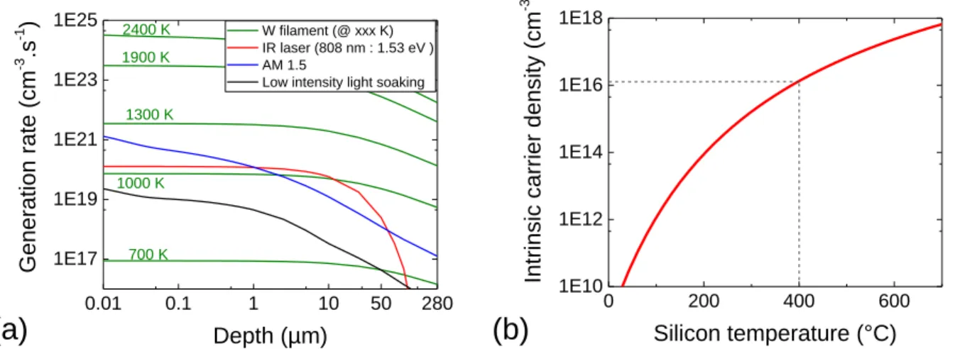
FIGURE 2.11:(A)GENERATION RATE AS A FUNCTION OF DEPTH FOR DIFFERENT ILLUMINATION PARAMETERS REPORTED IN LITERATURE. (B) EFFECTIVE LIFETIME BEFORE AND AFTER AN ILLUMINATION OF AN N-TYPE C-SI SAMPLES PASSIVATED BY 10NM OF AL2O3 DEPOSITED AT 200 °C AND ACTIVATED AT 380 °C FOR 5 MIN.400S ILLUMINATION AT A PHOTON FLUX OF 4.94·1017CM-2.S-1 (@1.53 EV). ... 35
FIGURE 2.12:LIFETIME’S FOLLOW-UP OF SET N°1 ALONG AM1.5ILLUMINATION ONE FACE A TIME (A) P-TYPE C-SI SUBSTRATE.(B) N-TYPE C-SI SUBSTRATE.LINES CORRESPOND TO THE FIT OF DATA ACCORDING TO EQUATION (2.25).WAFERS WERE PASSIVATED AT 200 °C WITH 100 ALD CYCLES AND ACTIVATED BY A PDA OF 5MIN AT 380 °C.THE BLUE DOTS AFTER DARK STORAGE SHOW THE FACT THAT PHOTO-INJECTED CHARGES ARE RELEASED FROM THE AL2O3 DURING THE STORAGE. ... 37
FIGURE 2.13:LIFETIME’S FOLLOW-UP OF SET N°2 ALONG AM1.5ILLUMINATION ON EACH FACE BEFORE MEASUREMENT.LINES CORRESPOND TO THE FIT OF DATA ACCORDING TO EQUATION (2.25).WAFERS WERE PASSIVATED AT 200 °C WITH 100 ALD CYCLES AND ACTIVATED BY A PDA OF 5MIN AT 380 °C.THE BLUE DOTS AFTER DARK STORAGE SHOW THE FACT THAT PHOTO-INJECTED CHARGES ARE RELEASED FROM THE AL2O3 DURING THE STORAGE. ... 38
FIGURE 2.14:(A)SCHEMATIC VIEW OF THE LOW INTENSITY BIFACIAL ILLUMINATOR.(B) TRANSMISSION SPECTRUM OF PLASTIC BOX AND NITROGEN BAG. ... 40
FIGURE 2.15:(A)PHOTON FLUX REACHING THE SAMPLES SURFACES.(B)GENERATION RATES IN THE SILICON VOLUME. ... 40
FIGURE 2.16:LIFETIME EVOLUTION IN THE LIBI FOR P-TYPE AND N-TYPE SAMPLES PASSIVATED BY 100 ALD CYCLES OF AL2O3 DEPOSITED @ 200 °C AND ACTIVATED FOR 5MIN @380 °C. ... 41
FIGURE 2.17:(A) STAINLESS-STEEL SHADOW MASK WITH OPTICAL FILTERS MOUNTED ON IT.THE MASK COVERS THE SAMPLE DURING THE FULL DURATION OF THE ILLUMINATION.LETTERS FROM A TO E ARE THE DIFFERENT LOCATIONS OF FILTERS:A IS NO FILTER,B:3.44EV; C:2.88EV;D:2.28EVE:1.28EV.(B) GENERATION RATE DEPTH PROFILES FOR MASK LOCATION A TO E. ... 43
FIGURE 2.18:(A) PCD CALIBRATED PHOTOLUMINESCENCE PICTURE OF THE LIFETIME SAMPLE AFTER 160H OF ILLUMINATION.(B) PASSIVATION RESULTS FOR THE FIVE DIFFERENT LOCATIONS RECEIVING DIFFERENT PHOTON ENERGY. ... 44
FIGURE 2.19:(A)GENERATION RATE DEPTH PROFILES FOR DIFFERENT W FILAMENT TEMPERATURES AND OTHER LIGHT SOURCES AS REFERENCES.(B)EFFECT OF TEMPERATURE ON THE INTRINSIC SILICON FREE CARRIER CONCENTRATION. ... 46
FIGURE 2.20:(LEFT)CONVENTIONAL CONFIGURATION OF THE FURNACE WITH A SIC COATED GRAPHITE HOT PLATE.(RIGHT)NEW CONFIGURATION OF THE FURNACE WITH A TRANSPARENT PLATE. ... 47
FIGURE 2.21:(A)CALCULATED ENERGY LEVELS AND OCCUPANCY FOR THE INTRINSIC POINT DEFECTS IN Α-AL2O3, AND CARBON CONTAMINATION POINT DEFECTS.ADAPTED FROM [3,4](B) SWITCHING CHARGE-STATE LEVELS OF OXYGEN RELATED DEFECTS IN Α-AL2O3, ADAPTED FROM [3,11]. ... 48
FIGURE 3.1:SCHEMATIC OF A GEOMETRICALLY ASYMMETRIC RFCCP REACTOR. ... 53
FIGURE 3.2:ENERGY FLOW IN DISCHARGE PLASMAS [21] ... 54
FIGURE 3.3: THE MVS CLUSTER TOOL... 55
FIGURE 3.4:FULL-FACTORIAL DOE RESULTS CONCERNING INTENSITY OF SIH* AND NH* EMISSION LINES AND VPL ... 57
FIGURE 3.5:(A)OES OF THE OF DIFFERENT PLASMA CONDITIONS.(B)OPTICAL PROPERTIES OF A-SINX:H DEPOSITED AT 53 PA WITH A POWER DENSITY OF 36MW.CM-2 AND A GAS RATIO FROM 1 TO 9. ... 58
FIGURE 3.6:REFLECTANCE MEASUREMENTS OF DOUBLE SIDE POLISHED WAFERS WITH BARE SURFACES OR AL2O3/A-SINX:H STACKS AND RANDOM PYRAMID TEXTURED SURFACES WITH AL2O3/A-SINX:H STACK.THE REFLECTANCE INCREASE BETWEEN THE DASH LINE AND THE WAVELENGTH OF 1107NM IS DUE TO THE BACK SURFACE REFLECTIVITY. ... 59
FIGURE 3.7:(A)ERDA AND TDS(INSET) SPECTRA;(B)FTIR SPECTRUM.PEAK 1 IS SI-H STRETCHING (2160CM-1); PEAK2 IS CO2 STRETCHING
(2340CM-1 AND 2360CM-1); PEAK3 IS N-H STRETCHING (3365CM-1)[26]. ... 60 FIGURE 3.8:EFFECTIVE LIFETIME OF N-TYPE C-SI PASSIVATED BY AN A-SINX:H DEPOSITED WITH THE OPTIMAL PROCESS CONDITION DEPOSITED,
EITHER ON HF CLEANED WAFER OR DIRECTLY ON NATIVE OXIDE.LIFETIMES ARE REPORTED FOR A CARRIER DENSITY OF 1015CM-3.60 FIGURE 3.9:(A)SHADOW MASK WITHOUT OPTICAL FILTERS.(B) LIFETIME SAMPLE PASSIVATED BY 60 ALD CYCLES OF AL2O3@250 °CPDA
@380 °C FOR 30MIN ON BOTH SURFACES.THE A-SINX:H CAPPING HAS BEEN DEPOSITED ONLY ON THE HALF OF THE TOP
SURFACE, NOT ON THE BACK SURFACE, THEN A PCA OF 20MIN @380 °C WAS CARRIED OUT.(C) PCD CALIBRATED
PHOTOLUMINESCENCE MAPPING OF THE LIFETIME SAMPLE AFTER 264H IN THE LIBI. ... 61 FIGURE 3.10:PROCESS FLOW USED TO PRODUCE LIFETIME SAMPLES.NUMBERS BETWEEN BRACKETS ARE PARAMETER RANGES THAT HAVE BEEN
TESTED.BEFORE PDA, THE WAFERS WERE CUT IN 4 PIECES TO PRODUCE 4 DIFFERENT LIFETIME SAMPLES. ... 62 FIGURE 3.11:(A)HYDROGEN CONTENT AND EVOLUTION IN THE AL2O3/A-SINX:H PASSIVATION STACK AS A FUNCTION OF AL2O3 PARAMETERS.
(B)IMPACT OF PDA TEMPERATURE ON AL2O3 ... 63
FIGURE 3.12:(A) LIFETIME FOLLOW-UP OF A SAMPLE PASSIVATED WITH 200 ALD CYCLES DEPOSITED @250 °C AND ACTIVATED AT 380 °C, LINE IS A GUIDE TO THE EYE.(B) INITIAL LIFETIME OF AL2O3/A-SINX:H PASSIVATION STACKS AS A FUNCTION OF AL2O3 THICKNESS
(ABSCISSA) AND DEPOSITION TEMPERATURE (ORDINATE) FOR THE PDA OF 350 °C.(C) SATURATED LIFETIME, AFTER LIFE2 IN THE
LIBI.(D) LIFETIME AFTER STORAGE IN THE DARK CABINET.BLACK LINE DELIMITS AREAS WITH SRV<10CM.S-1I.E. LIFETIME HIGHER THAN 1300µS... 64 FIGURE 3.13: ΤEFF ENHANCEMENT DUE TO LIFE2 TREATMENT (LEFT COLUMN), SATURATED ΤEFF(CENTRAL COLUMN) AND DEGRADATION OF THE
SATURATED ΤEFF DURING DARK STORAGE (RIGHT COLUMN) AS A FUNCTION OF AL2O3 THICKNESS AND DEPOSITION TEMPERATURE.
THE DIFFERENCE BETWEEN EACH ROW IS THE PDA TEMPERATURE BEFORE A-SINX:H CAPPING AS INDICATED ON THE RIGHT SIDE OF
ROWS.THE SCALE ABOVE COLUMNS STAND FOR THE FOUR GRAPHS OF THE COLUMN.BLACK LINES ON THE CENTRAL COLUMN GRAPHS REPRESENT AREAS WITH ΤEFF HIGHER THAN 1300µS, I.E.SRV<10CM.S
-1.O
N THE RIGHT COLUMN, BLACK LINES DELIMIT AREAS WHERE THE DEGRADATION DURING THE DARK STORAGE IS LOWER THAN 10 %... 66 FIGURE 3.14:AL2O3/A-SINX:H PASSIVATED SAMPLE PRESENTING BLISTERING. ... 67
FIGURE 3.15:SCHEMATIC SUMMARY OF PASSIVATION TRENDS FOR AL2O3/A-SINX:H PASSIVATED SAMPLES. ... 68
FIGURE 4.1:BLISTERING IMAGES FROM AL2O3/A-SINX:H STACKS (LEFT COLUMN SEM TILTED TOP-VIEW; RIGHT COLUMN OPTICAL
MICROSCOPE).(A) AND (B) MACROSCOPIC VIEW OF THE SURFACE.(C) INTACT BLISTER,(D) EXPLODED BLISTER,(E) ZOOM ON THE EXPLODED BLISTER SHOWING A STAMP-LIKE PATTERN (F) UNEXPLODED BLISTER ON TOP AND FULLY EXPLODED ONE,(G) BLISTER OF AL2O3/A-SINX:H STACKS NEAR THE EDGE OF THE SAMPLE, WERE A-SINX:H CAPPING IS NOT DEPOSITED. ... 70
FIGURE 4.2:(A)BLISTERING OF TYPE I AND TYPE II ON THE SAME SURFACE OBSERVED BY OPTICAL MICROSCOPE (100 ALD CYCLES DEPOSITED @ 200 °C AND CAPPED WITH 75NM OF A-SINX:H);(B) CONFOCAL PICTURE OF TYPE I BLISTER... 71
FIGURE 4.3:HIGH MAGNIFICATION PCD CALIBRATED PHOTOLUMINESCENCE PICTURE OF A BLISTERED SAMPLE (300 ALD CYCLES OF AL2O3
CAPPED BY 75NM OF A-SINX:H).DARK SPOTS ARE BLISTERS; THE BIG RING IS THE SINTON STAGE DETECTOR.THE SQUARE IN THE
MIDDLE IS A ZOOM OF THE TOP LEFT CORNER SQUARE. ... 72 FIGURE 4.4:(A)TDS OF AL2O3 DEPOSITED AT DIFFERENT TEMPERATURES (1000 ALD CYCLES).(B) AND (C) OPTICAL MICROSCOPE PICTURE OF
BLISTERS THAT APPEAR DURING TDS FOR AL2O3 DEPOSITED AT 150 °C AND 200 °C RESPECTIVELY.AX10 ZOOM OF BLISTERS IS
VISIBLE IN THE TOP RIGHT CORNER OF EACH PICTURE.BLISTERS PRESENTED IN THE ZOOM OF (B) ARE TOTALLY EXPLODED, THE SILICON SURFACE IS EXPOSED TO THE ATMOSPHERE. ... 73 FIGURE 4.5:(A)BLISTERING MAP OF THE AL2O3/A-SINX:H PASSIVATION STACK DEPENDING ON AL2O3 THICKNESS AND DEPOSITION
TEMPERATURE.THE A-SINX:H CAPPING IS 75NM THICK.(B)TYPE I BLISTERING DENSITY FOR THE STACK HAVING 60 ALD CYCLES OF
AL2O3 CAPPED BY 75NM OF A-SINX:H. ... 74
FIGURE 4.6:TYPE II BLISTERING STATISTICS FOR 100 AND 200 ALD CYCLES CAPPED BY 75NM OF A-SINX:H.DETERMINED WITH AN OPTICAL
MICROSCOPE. ... 76 FIGURE 4.7:(A) SELECTION OF NON-HOMOGENEOUSLY DELAMINATED BLISTERS OBSERVED WITH OPTICAL MICROSCOPE.(B) CONFOCAL
MAPPING OF A NON-HOMOGENEOUSLY DELAMINATED BLISTER. ... 77 FIGURE 4.8:(A)SCHEMATIC DIAGRAM OF APIC SETUP:THE PUMP BEAM IS CHOPPED AT HIGH FREQUENCY (100KHZ) THANKS TO AN
ACOUSTO-OPTIC MODULATOR (AOM).THE REFLECTED PROBE BEAM IS DETECTED BY AN OPTICAL DETECTOR AND THE SIGNAL IS AMPLIFIED THROUGH A LOCK-IN SCHEME IN ORDER TO EXTRACT THE RELATIVE CHANGE IN REFLECTIVITY (ΔR/R= TRANSIENT REFLECTIVITY) AT THE C-SI SURFACE.(B)SCHEMATIC REPRESENTATION OF THE ACOUSTIC WAVE PROPAGATION IN THE PASSIVATION STACK, FOR THE SAKE OF CLARITY, PHENOMENA THAT ARE TEMPORALLY SEPARATED ARE DRAWN SHIFTED TO THE RIGHT (DOTTED BLACK ARROWS ARE TEMPORAL TRANSLATION, NOT SPATIAL).AN ACOUSTIC WAVE IS GENERATED AT THE SAMPLE SURFACE WITH THE PUMP LASER (T0).THE WAVE PROPAGATES THROUGH THE DIELECTRIC STACK (RED ARROW) TOWARD THE AL2O3/C-SI
INTERFACE.THERE, A PART OF THE ACOUSTIC WAVE IS TRANSMITTED TO THE C-SI SUBSTRATE AND THE OTHER PART IS REFLECTED BACK (1ST POINT).THE PROPAGATION OF THE ACOUSTIC WAVE THROUGH THE AL2O3/C-SI INTERFACE MODIFIES THE C-SI SURFACE
WHICH PROPAGATES TOWARD THE FREE SURFACE IS FULLY REFLECTED AT THE AIR/AL INTERFACE AND PROPAGATES AGAIN TOWARD THE C-SI/AL2O3 INTERFACE PRODUCING A 2
ND
ECHO DETECTED AT T2.THIS REFLECTION SCHEME IS REPEATED UNTIL THE ACOUSTIC
WAVE ENERGY IS FULLY DISSIPATED.(C)RECORDED SIGNAL FROM THE ACOUSTIC WAVE GENERATION (T0) TO THE TOTAL WAVE
DISSIPATION (T0+200PS).THE TIME DELAY OF 36PS BETWEEN EACH ECHO DETECTION (T1T2T3 ETC.) CORRESPONDS TO THE
ROUND TRIP OF THE ACOUSTIC WAVE BETWEEN THE AIR/AL INTERFACE AND THE AL2O3/C-SI INTERFACE. ... 78
FIGURE 4.9:(A) TRANSIENT REFLECTIVITY SIGNAL RECORDED FOR TWO SAMPLES.(B) DETERMINATION OF THE REFLECTIVITY COEFFICIENT (RA)
FROM THE SIGNAL RECORDED FOR THE TWO SAMPLES OF GRAPH (A).THE NORMALISED INTENSITY OF THE ECHO IS FITTED WITH A POWER LOW RN
.THE RESULTS ARE PRESENTED IN TWO WAYS IN THIS THESIS:(C) A 900 POINTS MAPPING OF THE REFLECTIVITY COEFFICIENT DETERMINED OVER A SURFACE OF 150 X 150 µM.THE STEP BETWEEN MEASUREMENT POINTS (BLACK DOT) IS 5µM FOR A LASER SPOT AREA SMALLER THAN 1µM².(D) STATISTICAL BOX CHARTS ARE USED TO SUMMARISE THE 900 MEASURED VALUES OF A RA MAPPING. ... 79
FIGURE 4.10:APIC MAPPING OF THE AL2O3/C-SI INTERFACE FOR 60 ALD CYCLES (LEFT COLUMN) AND 100 ALD CYCLES (RIGHT COLUMN)
DEPOSITED AT 150 °C,200 °C AND 250 °C ANNEALED AT 350 °C FOR 30 MINUTES. ... 80 FIGURE 4.11:APIC MAPPING OF THE AL2O3/C-SI INTERFACE FOR 60ALD CYCLES (LEFT COLUMN) AND 100ALD CYCLES (RIGHT COLUMN)
DEPOSITED AT 150 °C,200 °C AND 250 °C ANNEALED AT 410 °C FOR 30 MINUTES. ... 81 FIGURE 4.12:REFLECTION COEFFICIENT DISTRIBUTION OF THE AL2O3/C-SI INTERFACE FOR 6NM AND 10NM OF AL2O3 DEPOSITED AT 150 °C,
200 °C AND 250 °C.THE PDA OF 30 MINUTES WAS CARRIED OUT AT (A)350 °C(B)410 °C. ... 82 FIGURE 4.13:CROSS-SECTIONAL VIEW OF THE MODELLED “PICOSUN R200” ARCHITECTURE... 84 FIGURE 4.14:MODELLED TEMPERATURE EVOLUTION OF THE C-SI SUBSTRATE VERSUS TIME.THE SUBSTRATE-HOLDER AND THE SILICON
SUBSTRATE ARE INTRODUCED AT ROOM TEMPERATURE IN A PICOSUN ALD SYSTEM HEATED AT 300 °C. ... 85 FIGURE 4.15:(A)EXPERIMENTAL TEMPERATURE PROFILES MEASURED ON THE SUBSTRATE WITH NON-REVERSIBLE TEMPERATURE LABELS, LINES
ARE GUIDES TO THE EYES SHOWING TEMPERATURE EVOLUTION DURING THE DEPOSITION PROCESS.(B)AS-DEPOSITED LIFETIME FOR STANDARD ALD AND TD-ALD WITH PROFILE #1 AND PROFILE #2.LINES ARE A GUIDE TO THE EYES. ... 86 FIGURE 4.16:MINORITY CARRIER LIFETIME OF SAMPLE N-TYPE,FZ<111>,DSP WAFERS, BOTH SIDES PASSIVATED BY ~20NM OF A-SI:H AFTER
30S OF HF.DOUBLE SIDE ILLUMINATION DURATION IN THE LIBI WAS CONDUCTED FOR 64H. ... 87 FIGURE 4.17:LIFETIME RESULTS OF AL2O3/A-SINX:H PASSIVATION STACKS FOR STANDARD ALD AND TD-ALD(PROFILE #1) WITH DIFFERENT
PDA(A) SATURATED LIFETIME (B) LIFETIME ENHANCEMENT DUE TO LIFE2.LINES ARE GUIDES TO THE EYE. ... 89
FIGURE 4.18:(A)APIC MAPPING OF THE AL2O3/C-SI INTERFACE FOR 60 TD-ALD CYCLES (PROFILE #1) THAT RECEIVED A PDA OF 30 MIN AT 380 °C BEFORE CAPPING AND PCA.(B) REFLECTION COEFFICIENT DISTRIBUTION OF THE AL2O3/C-SI INTERFACE FOR 60 ALD
CYCLES DEPOSITED AT CONSTANT TEMPERATURE (150 °C,200 °C AND 250 °C) AND TD-ALDWITH TEMPERATURE PROFILE#1... 90 FIGURE 5.1:(A)CALCULATED ENERGY LEVELS AND OCCUPANCY FOR THE INTRINSIC POINTS DEFECT IN SI3N4.[25](B)SWITCHING CHARGE
-STATE LEVELS OF DANGLING BONDS IN SI3N4.[25,27,28] ... 95
FIGURE 5.2:(A) POSITION OF THERMODYNAMIC TRANSITION LEVELS IN AL2O3 AND IN A-SINX:H FOR INTRINSIC AND EXTRINSIC POINT DEFECT
LEVELS ARISING FROM ATOMS INCLUSION OF THE AL2O3 FILM IN THE A-SINX:H FILM AND VICE VERSA [5,6].(B) SCHEMATIC OF
ELECTRONIC DEFECTS LOCATION IN AN AL2O3/A-SINX:H PASSIVATION STACK.POINT DEFECTS SUSPECTED TO CAPTURE ELECTRONS
IN AL2O3 ARE SUPPOSED TO BE LOCATED IN THE FIRST NANOMETRE ABOVE THE SURFACE.THE X VALUE REPRESENTS THE AL2O3
FILM THICKNESS, FROM 2NM TO 20NM.THE AL2O3/A-SINX:H INTERFACE TRANSITION LEVELS ARE ALL THOSE OF FIGURE 5.2.A,
REFERRED AS AN “ELECTRONIC LADDER” IN THE TEXT.RED BARS SHOW THE TRANSITION LEVELS RELATED TO POSITIVE OR NULL CHARGE STATE, AND BLUE BARS SHOW THE TRANSITION LEVELS RELATED TO NULL OR NEGATIVE CHARGE STATE. ... 96 FIGURE 5.3:SCHEMATIC MODEL USED FOR SILVACO 1D SIMULATIONS... 97 FIGURE 5.4:EFFECTIVE LIFETIME AS FUNCTION OF THE INJECTION LEVEL FOR AL2O3/A-SINX:H PASSIVATION STACKS WITH AL2O3 THICKNESS OF
20NM, A-SINX:H THICKNESS OF 75NM. AND DIT(AL2O3/C-SI) OF 1011EV-1.CM-2.(A) AL2O3/A-SINX:H INTERFACE FREE OF FIXED
CHARGES (B) AL2O3/A-SINX:H INTERFACE WITH FIXED CHARGES DENSITY OF +1012CM-2. ... 98
FIGURE 5.5:SIMULATION RESULTS OF BAND BENDING AT THE C-SI SURFACE (TOP GRAPHS LINE, GREY LINE IS THE FLAT BAND CONDITION) AND RESULTING LIFETIME (BOTTOM GRAPH ROW, BLACK LINE IS EQUIVALENT TO SRV OF 10CM.S-1) FOR AN INJECTION LEVEL OF
1015CM-3.CAPITAL LETTERS ON THE TOP SCHEMATIC DIELECTRIC STACKS REPRESENT CHARGES DENSITY VALUES USED FOR SIMULATION.A=[-5·1010 TO -5·1012] CM-2;B= +1012CM-2;C= 2·1011CM-2 AND D= 0CM-2.THE BAND STRUCTURE ON THE TOP RIGHT CORNER SHOWS THE VSB DEFINITION. ... 99
FIGURE 5.6:(A) OPTICAL BANDGAP AND REFRACTIVE INDEX OF A-SIOX:H(DETERMINED BY SE) AS A FUNCTION OF THE CO2 TO SIH4 RATIO.
THE DEPOSITION TEMPERATURE IS 200 °C FOR BUFFER #1 AND 250 °C FOR BUFFER #2(B) SIMS PROFILES OF AS-DEPOSITED BUFFER #1 AND #2. ... 101
FIGURE 5.7:(A)EFFECTIVE LIFETIME (COLUMNS) AND LIFETIME IMPROVEMENT DUE TO LIFE2 IN THE LIBI(DOTS) FOR SAMPLES PASSIVATED
WITH 60 ALD CYCLES OF AL2O3, DEPOSITED AT 250 °C, CAPPED BY 75NM OF A-SINX:H(BLACK SYMBOLS, CONTROL GROUP) OR
BY A STACK COMPRISING 20NM OF A-SIOX(BUFFER #1 IN RED = GROUP #1, BUFFER #2 IN GREEN = GROUP #2) AND 55 NM OF A
-SINX:H.(B) ERDA SPECTRA OF BUFFER #1 AND #2(DEPOSITED DIRECTLY ON C-SI) AFTER FGA FOR 20NM OF BUFFER LAYERS #1
AND #2. ... 103 FIGURE 5.8:(A)BAND BENDING AT THE C-SI SURFACE AND (B) EFFECTIVE LIFETIME RESULTING FROM THE BAND BENDING FOR THE ALTERNATIVE
CASE #1(FIGURE 5.5) BUT WITH DIT SET AT 10
12
EV-1.CM-2. ... 104 FIGURE 5.9:MODELLED GROWTH RATE FOR AN INTER-ELECTRODE DISTANCE OF (A)20MM. AND (B) 30MM. ... 106 FIGURE 5.10:MODELLED SURFACE RESPONSES FOR AN INTER-ELECTRODE DISTANCE OF 20MM.(A) REFRACTIVE INDEX AT 633NM.(B)
EXTINCTION COEFFICIENT AT 300NM.(C)FIXED CHARGES DENSITY AFTER PCA.(D)HYDROGEN RELEASE BY PCA.FOR THE SAKE OF CLARITY, ONLY ONE SURFACE IS PLOTTED WHEN THE PRESSURE CHANGE DOES NOT STRONGLY IMPACT THE RESPONSE. ... 107 FIGURE 5.11:DOE RESULTS FOR THE OPTIMAL COMPROMISE BETWEEN REFRACTIVE INDEX (DESIRABILITY SET MAXIMAL FOR N=1.97),
EXTINCTION COEFFICIENT (DESIRABILITY SET AT MINIMISING K), FIXED CHARGE DENSITY (DESIRABILITY SET AT MINIMISING QF) AND
HYDROGEN RELEASE (DESIRABILITY SET AT MAXIMISING H2 RELEASE).NO DESIRABILITY RESTRICTIONS HAVE BEEN SET ON THE
CRITICAL ANGLE, THE PLASMA POTENTIAL (VPL), THE GROWTH RATE AND THE TOTAL HYDROGEN CONTENT IN ORDER TO GET THESE
VALUES WITHOUT IMPACTING THE OPTIMISATION. ... 108 FIGURE 5.12: ABSORPTION OF THE FORMER AND THE NEW A-SINX:H LAYERS CALCULATED FROM THEIR RESPECTIVE ABSORPTION COEFFICIENT
(DETERMINED BY SE).THE CALCULATED CURRENT DENSITY LOSS ASSOCIATED TO ABSORPTION ASSUMES ONE PASS OF THE PHOTONS IN THE FILMS AND NO REFLECTION AT THE INTERFACES. ... 110 FIGURE 5.13:EFFECTIVE LIFETIME OF AL2O3/A-SINX:H PASSIVATED SAMPLES WITH (A) 20 ALD CYCLES AND (B) 60 ALD CYCLES DEPOSITED
WITH THE THERMAL DRIFT PROFILE #1.THE SIMULATED CURVE WAS OBTAINED USING THE MODEL DEPICTED ON FIGURE 1.7 WITH AN INTERFACIAL TRAP DENSITY OF 1010EV-1CM-2 AND A QF OF -3·10
12
CM-2 AT THE C-SI/AL2O3 INTERFACE. ... 111
FIGURE 5.14:QSS-PC CALIBRATED PHOTOLUMINESCENCE PICTURE (ΔN=1015CM-3) OF A P-TYPE C-SI WAFER WITH THE OPTIMISED PASSIVATION STACK, I.E.60 ALD CYCLES USING THERMAL DRIFT PROFILE #1; ANNEALED 30 MIN @380 °C; CAPPED WITH THE NEW A-SINX:H BEFORE PCA. ... 112
List of Tables
TABLE 1.1:MODEL PARAMETERS USED FOR MOST COMMON MATERIAL IN THIS WORK ... 14
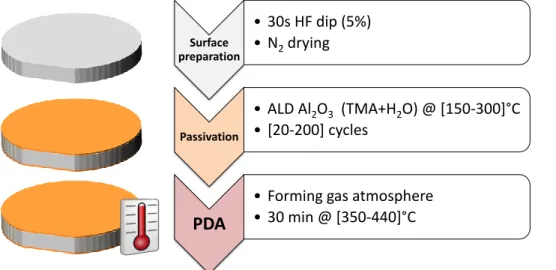
TABLE 2.1:ALD CYCLE USED IN THIS THESIS.DEPOSITION CHAMBER PRESSURE IS AROUND 10 PA AND CONTINUOUSLY FLOWED BY 600SCCM OF NITROGEN. ... 22
TABLE 2.2: COMPARATIVE AL2O3 PROPERTIES. ... 25
TABLE 2.3:TOPSIL SILICON SUBSTRATE CHARACTERISTICS ... 27
TABLE 2.4:ILLUMINATION EFFECT REPORTED IN THE LITERATURE ... 33
TABLE 2.5:EXPONENTIAL FIT RESULTS OF THE LIFETIME INCREASE FOR SET N°1 AND N°2 ... 39
TABLE 2.6:EXPONENTIAL DECAY FIT RESULTS OF THE LIFETIME EVOLUTION IN THE LIBI. ... 42
TABLE 2.7: HEAT TRANSFER MODE FOR SOME POPULAR RTP FURNACES. ... 45
TABLE 3.1:PECVD RECIPE FOR AN INTER-ELECTRODE DISTANCE OF 20MM ... 56
TABLE 4.1: PASSIVATION PARAMETERS OF N-TYPE,FZ<111>,DSP WAFERS, BOTH SIDES PASSIVATED AFTER 30S OF HF.THE THICKNESS IS MEASURED BY SE ... 87
TABLE 5.1:ALDCYCLE USED IN THE FLEXAL REACTOR.DEPOSITION CHAMBER IS OUT-GASSED AT 0.05 PA AFTER SUBSTRATE LOADING AND THEN THE DEPOSITION PRESSURE IS RAISED AROUND 11 PA. ... 100
TABLE 5.2:PECVD PARAMETERS FOR A-SIOX:H DEPOSITION.SET-POINT TEMPERATURE WAS 200 °C(165 °C MEASURED ON SUBSTRATE), THE INTER-ELECTRODE DISTANCE WAS 28MM AND THE RF FREQUENCY 40 MHZ. ... 101
TABLE 5.3:MATERIAL PROPERTIES OF BUFFER #1 AND BUFFER #2 ... 102
TABLE 5.4:BOX-BEHNKEN SURFACE RESPONSE DOE PARAMETERS ... 105
TABLE 5.5:QUALITY OF OUTPUT MODELS AND THE TWO MOST IMPACTING PECVD PARAMETERS ON THE DIFFERENT MODEL RESPONSES IN ORDER OF IMPORTANCE ... 106
TABLE 5.6:COMPARISON BETWEEN THE FORMER A-SINX:H PROCESS PARAMETERS AND THE NEW A-SINX:H PROCESS PARAMETERS OBTAINED FROM THE DOE DATA TREATMENT. ... 109
List of acronym and symbols
Unit
Definition
α cm-1 Absorption coefficient
Al2O3 Aluminium oxide
Al-BSF Aluminium back surface field
ALD Atomic Layer Deposition
AM1.5 Solar spectrum at an air mass of 1.5
APCVD Atmospheric Pressure Chemical Vapour Deposition
ARC Anti-reflection coating
a-Si:H Hydrogenated amorphous silicon
a-SiNX:H Hydrogenated amorphous silicon nitride
c-Si Monocrystalline Silicon
CB Conduction Band
CBM Conduction Band Minimum
COCOS Corona oxide characterisation of semiconductors
CSNSM Centre de Sciences Nucléaires et de Sciences de la Matière
CVD Chemical Vapour Deposition
Cz Czochralski
Dit eV
-1
.cm-2 Interfacial trap density
E04 eV optical bandgap energy
ε Material emissivity
η % Efficiency
ERDA Elastic recoil detection analysis
FF % Fill factor
FTIR Fourier transform infrared spectroscopy
FZ Float zone
σn cm
2
Electron capture cross
σp cm
2
Hole capture cross
G cm-3 Generation rate
GPC Å/cycle Growth per cycle
HF Hydrofluoric acid
IPVF Institut Photovoltaïque d'Île-de-France
Isc mA Short-circuit current
λ nm Wavelength
LIBI Low Intensity Bifacial Illuminator
LIFE2 Light Induced Field Effect Enhancement
LPICM Laboratoire de Physique des Interfaces et des Couches Minces
n Refractive index
NRA Nuclear Reaction Analysis
PA-ALD Plasma Assisted Atomic Layer Deposition
PCD Photoconductance decay
PECVD Plasma Enhanced Chemical Vapour Deposition
PERC Passivated emitter and rear cell
PL Photoluminescence
PV Photovoltaic(s)
Qf cm
-2
Fixed charge density
Ra (AU) Acoustic reflection coefficient
RBS Rutherford backscattering spectrometry
Reff % Effective reflectance
RF Radio Frequency
RH % Relative humidity
sccm Standard cubic centimetres per minute
Seff cm.s
-1
Effective Surface recombination velocity
SE Spectroscopic Ellipsometry
SEM Scanning electron microscopy
SIMS Secondary Ion Mass Spectrometry
Seff cm2.s−1 Effective surface recombination velocity
SQL Shockley–Queisser limit
SRH Shockley–Read–Hall
SRV Surface recombination velocity
τeff µs Effective lifetime
θc ° critical angle
TDS Thermal desorption spectroscopy
TD-ALD Thermal Drift Atomic Layer Deposition
Th-ALD Thermal Atomic Layer Deposition
TMA Trimethylaluminium
U cm-3 Recombination rate
UV Ultraviolet
VB Valence Band
VBM Valence Band Maximum
VDC V Self-bias voltage
VPL V plasma potential
VRF V Potential at the RF electrode
Vsb eV Surface barrier potential
Voc mV Open-circuit voltage
Introduction
Solar energy outlook
In the 21st century, the energy access remains a major source of inequality around the world, leaving billions of people without electricity or without access to clean cooking facilities (Figure 0.1) [13]. Among all the continents, Africa is the one that requires the most intensive energy deployment because contrary to Asia, its demographic transition just begun. African people were 1.26 billion in 2015, representing only 17 % of the world population while in 2100 they will rise to 4.47 billion, representing 40 % of the world population and so a proportional energy demand [41]. The African continent is plenty of fossil resources that used to be extracted from their soil for centuries, but it also benefits from the largest solar power reaching the ground (Figure 0.1). It has to be reminded that the solar energy reaching earth can yearly cover more than 1000 times the world needs in energy [42].
Figure 0.1: Number of people without access to electricity or to proper cooking facilities around the world [13]. Data are reported on the world solar resource map (Global Horizontal Irradiation) [36]. Africa 634 India China Developing Asia South America 22 162 414 0 65 793 244 819 453 <800 1200 1600 2000 2400 2800 kWh/m² (annual sum)
: Population without electricity access (millions)
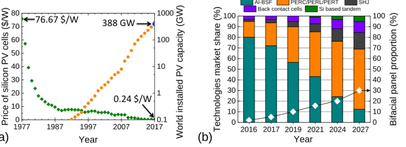
The solar energy has been used for its heat for millennia, from the ignition of the Olympic flame in the 3rd century B.C. to the vapour generation that powers electrical turbines nowadays [43]. However, the direct conversion of the sunlight into electricity, named the photovoltaic (PV) effect, has been reported only in 1839 by the French scientist Alexandre-Edmond Becquerel [44]. It took another century to create reliable devices that can be commercialised, but at prices that were not competitive for the mass production of electricity at that time (Figure 0.2.a). The reduction of the $/W ratio made the PV deployment possible in the late ‘90s. Thanks to technology’s advances and mass production, the price per watt has been divided by ~320 in 40 years, allowing a world total installed capacity of about 388 GW by the end of 2017 (Figure 0.2.a). Despite this exceptional growth rate of the PV market, PV electricity represents only 1.5 % of the world electrical generation at the end of 2016 [45]. Further cost reduction and technological improvement are required to support the fast growth of PV.
Many different types of photovoltaic solar cells have been developed over time, but these based on crystalline silicon (c-Si) have supplanted all the others, representing more than 93 % of the market at the end of 2016 [46]. Inside this market there is still a wide variety of technologies adopting different architectures. The ‘Aluminium-Back Surface Field’ (Al-BSF) is the mainstream one (Figure 0.2.b) because it is the simplest and the cheapest to manufacture.
Figure 0.3: (a) Band structure of Al-BSF where VB stands for valence band and CB for conduction band (b) Schematic cross section of Al-BSF and PERC solar cells.
E (eV) X h+ e -VB CB n+ p+ p Full BSF local BSF Electrical contact Electrical contact
Passivation & Antireflection
Passivation
Al-BSF PERC
(a)
(b)
Figure 0.2: (a) Price of the c-Si photovoltaic cells (left axis) and World installed PV capacity (right axis) [32, 33]. (b) Market share forecasts for the main solar cells architectures and proportion of bifacial solar modules [38].
1 2 3 4 5 6 0 10 20 30 40 50 60 70 80 90 100 2027 2024 2021 2019 2017 Technolog
ies market share (%)
Year
Al-BSF PERC/PERL/PERT SHJ
Back contact cells Si based tandem
2016 0 10 20 30 40 50 60 70 80 90 100 Bifacial panel propo rtion (%) 1977 1987 1997 2007 2017 0 10 20 30 40 50 60 70 80 Price of sili con PV cells ($/W) Year 0.1 1 10 100 1000 World in stalled PV capaci ty (G W) (a) (b) 76.67 $/W 0.24 $/W 388 GW
The Al-BSF maximum conversion efficiency seems to be around 20 % while its upgraded architecture PERC (Passivated Emitter and Rear Cell) is already promising 24 % [47-49]. Naturally the Al-BSF should give way to the PERC architecture and its variants in the next decade. In addition, these architectures are also compatible with the second market trend which is the adoption of bifacial architectures. The light collection on the back surface of the solar cells takes advantage of the albedo, increasing the system relative efficiency up to 30 % [50, 51].
The Al-BSF architecture consists in a p-type absorber with a bipolar p-n+ junction on top and a unipolar p-p+ junction below. These junctions result in the band structure shown on Figure 0.3.a that allows carrier separation and diffusion to the electrical contacts located on the top for electrons and at the bottoms for holes. The unipolar junction at the bottom is formed by alloying aluminium to the lowly doped absorber and gives its name to the architecture: Aluminium Back-Surface Field [52]. On the front surface there is an antireflection coating (ARC) on a textured surface to maximise photon collection. This layer also serves as surface passivation, which is a technological key element to master in order to continue the photovoltaic development. Its implementation on the back surface of solar cells such as in the PERC architecture (Figure 0.3.b) opened the route to higher conversion efficiency.
Thesis aim and outline
This doctoral work is dedicated to the fundamental understanding and improvement of c-Si surface passivation by aluminium oxide (Al2O3) and its related derivative stacks. It is part of the
‘advanced silicon technologies’ project conducted by the ‘Institut Photovoltaïque d’Île-de-France’ (IPVF). This project aims to develop a c-Si solar cell architecture fully processed at low temperature, i.e. lower than 400 °C, and that has a conversion efficiency higher than 20 %.
The first chapter reminds the physics key points of passivation and its link with the solar cell efficiency. Then, a brief description of the mainstream characterisation techniques used in this work is done.
The second chapter deals with the deposition technique and the material properties of Al2O3 films. The atomic layer deposition is described and the impacts of process
conditions on film properties are investigated. The sensitivity of the passivation properties to post-deposition illumination is addressed in this chapter.
The third chapter is dedicated to the passivation properties of Al2O3 films embedded in
a stack with hydrogenated amorphous silicon nitride (a-SiNX:H). The
plasma-enhanced chemical vapour deposition technique is described and the impact of process conditions on film properties is investigated. The passivation stability over time of Al2O3/a-SiNX:H stacks is studied in this chapter.
The fourth and the fifth chapters investigate passivation degradation mechanisms related to Al2O3/a-SiNX:H stacks. First, the fourth chapter address the degradation
occurring at the c-Si/Al2O3 interface, i.e. blistering. Then, the fifth chapter explores
the impact of a-SiNX:H capping on the electrostatic properties of the passivation stack.
Finally, this work is summarised in a conclusion section, which summaries our achievements and provides further research perspectives.
5
Chapter
1
1
Theoretical and experimental context
Contents
1.1 SOLAR CELLS PHYSICS... 6
1.1.1 Device performance ... 6
1.1.2 Recombination ... 7
1.1.3 Passivation ... 8
1.1.4 The effective lifetime of minority carriers ... 10
1.2 CHARACTERISATION TECHNIQUES ... 12
1.2.1 Electrical properties ... 12
1.2.1.1 Photoconductance decay... 12
1.2.1.2 PCD calibrated photoluminescence mapping ... 13
1.2.1.3 Corona Oxide Characterization Of Semiconductor ... 13
1.2.2 Optical properties ... 14
1.2.2.1 Spectroscopic ellipsometry ... 14
1.2.2.2 Spectrophotometry ... 15
1.2.3 Material properties ... 16
1.2.3.1 X-ray Reflectometry ... 16
1.2.3.2 Ion beam analysis technique ... 18
1.2.3.3 Thermal Desorption Spectroscopy ... 18
1.2.3.4 Vibrational spectroscopy ... 18
1.1
Solar cells physics
1.1.1
Device performance
The solar cells power conversion efficiency (η) as defined by equation (1.1) cannot exceed 29.4 % for a single bandgap material like silicon [53]. Indeed, photons having energy greater than the bandgap will lose the difference by thermalisation while photons with energy lower than the bandgap will not be absorbed. For a more complete description of the solar cells physics, the reader may refer to the book by Peter & Uli Würfel [54], while we focus here on parameters relevant to understand the surface passivation.
η =ISC∙ VOC∙ FF
Pin (1.1)
With:
• ISC : the short-circuit current • VOC : the open-circuit voltage
• FF : the fill factor
• Pin : the incoming solar power
As previously mentioned, the conversion efficiency of 29.4 % has never been reached so far due to several losses among which photo-generated carrier recombination is one of the most important. Electrons and holes can recombine by different mechanisms (see next section) reducing the three numerator factors of the equation (1.1) numerator. In the case of a constant photon flux reaching the silicon surface, the electron-hole pair generation rate (G) in the silicon can be assumed constant over time. The carrier density (Δn) is then only proportional to the recombination rate (R) in the device. The VOC is the most impacted by the carrier recombination
as its value is proportional to the photo-generated carrier density in silicon. For a p-type c-Si cell with a dopant density NA, the VOC can be expressed by equation (1.2). The passivation aims to
reduce the recombination in a solar cell and its quality is often judged after the solar cell VOC.
VOC =kT q ln (
(NA+ Δn)Δn
ni2 ) (1.2)
With:
• k : the Boltzmann constant
• T : the absolute temperature
• q : the elementary charge
• ni : the intrinsic carrier density
1.1.2
Recombination
Recombination can be divided in two terms, the one that is intrinsically linked to the use of semiconductors and the one that is due to external factors.
Regarding intrinsic recombination mechanisms, the first one is the radiative recombination process which is the exact opposite of the photo-generation (Figure 1.1.a). An electron-hole pair recombines, emitting a photon with an energy equal to the bandgap value. Due to the indirect bandgap nature of silicon, a phonon is required to assist the reaction, decreasing the recombination rate importance associated to this mechanism. The second mechanism is the Auger recombination which involves the interaction of three carriers. It consists in the recombination of an electron from conduction band and a hole from the valence band, but rather than a photon emission, the energy is transferred to a third free carrier. This one can be either an electron in conduction band (eeh process, Figure 1.1.b) or hole in the valence band (ehh process, Figure 1.1.c). The newly exited carrier then thermalises back to the band edge.
Regarding extrinsic recombination, the one occurring through defects, named Shockley-Read-Hall (SRH) recombination [55], is directly linked to the crystalline quality of the silicon. The SRH process occurs via discrete energy levels (Et) present in the bandgap that provide
intermediate states available for electrons and holes recombination in a two, or more steps (Figure 1.1.d). These intermediate levels, designated as traps, are introduced by point defects (vacancy, interstitial atoms, substitutional atoms), 2D defects (dislocations), 3D defects (complexes, precipitates) and by the interaction between these defects. By controlling the crystal purity and quality, SRH recombination in the bulk of silicon can be strongly limited while there is another similar recombination mechanism that will remain even for a perfect silicon crystal. Silicon wafer surfaces are a brutal interruption of the crystalline lattice periodicity and are thus two dimensions defects. Indeed, silicon surface atoms do not have their 4 neighbours, so they present one or more electronic orbitals that are not participating in bonding and are named dangling bonds. Surface dangling bonds generate a high quantity of trap levels continuously distributed over the bandgap, providing a very efficient non-radiative recombination pathway (Figure 1.1.e).
Figure 1.1: Schematic representation of (a) radiative recombination; (b) Auger recombination involving eeh (c) ehh; (d) SRH recombination and (e) surface recombination h e h e e h e h hν VB CB (a) (b) (c) h e h e (d) (e) Et surface
The surface recombination rate (Usurf) can be expressed by equation (1.3). Depending on their
energy levels in the bandgap, traps catch more or less efficiently one type of carriers. A capture cross-section for holes (σp) and electrons (σn) is defined for each type of traps. Traps with
energies close to the centre of the bandgap are the most effective recombination centres, designated as deep defects in opposition to the shallow defects with energy levels near band edges. Usurf= ∫ νth(nSpS− ni2) nS+ n1(Et) σp (Et) + pS+ p1(Et) σn(Et) ∙ Dit(Et) ∙ dEt EC EV (1.3) n1= niexp Et− Ei k𝐵T (1.4) p1= niexp Et− Ei k𝐵T (1.5) With:
• νth : the thermal velocity of charge carriers, assumed identical for electrons and holes
• ns : the electron concentration at the surface
• ps : the hole concentration at the surface
• ni : the intrinsic carrier density
• n1 : statistical factor as defined by equation (1.4)
• p1 : statistical factor as defined by equation (1.5)
• Et : the energy level of the trap
• Dit : the interfacial trap density
• T : the temperature
• k𝐵 : the Boltzmann constant
• E𝑖 : the intrinsic energy level of the trap
1.1.3
Passivation
As commonly used in metallurgy, surface passivation aims to prevent degradation mechanism of the material properties. Concerning silicon, passivation designates more the inhibition of recombination mechanisms in order to preserve its electronic properties, rather than preventing its corrosion. As intrinsic recombination processes are unavoidable, silicon passivation aims at reducing extrinsic recombination. While SRH recombination occurring in the volume of silicon can be greatly reduced by enhancing the quality of the metallurgical processes, the presence of surfaces and so surface recombination cannot be avoided. In fact, the large surface to volume ratio of silicon solar cells makes surface recombination a limiting factor to conversion efficiency. From equation (1.3), it can be seen that there are two approaches to reduce surface recombination.
The first approach consists in the reduction of the Dit and is named the chemical passivation.
To remove energy states introduced in the bandgap by dangling bonds, one just has to satisfy this bonding requirement, as oxygen is doing when native oxide is growing at the silicon surface. The bandgap difference between silicon (1.12 eV @ 300 K) and its oxide (8.9 eV @ 300 K) is high enough to keep carriers within the silicon. However, the uncontrolled growth of native oxide on silicon surface generates a defective layer that has trap levels in its bandgap (Figure 1.2). The native oxide does not provide an efficient surface passivation and has to be replaced by another material.
The second passivation approach consists in the reduction of either majority or minority carrier density at the surface and is named the field effect passivation. In order to repel one type of carrier from the surface, energy band bending can be set-up using a doping profile below the surface, as it is done on the Al-BSF back-surface. Another way is to use electrostatic charges deposited on the surface, e.g. corona charges [56], or embedded within an insulator material deposited on the surface. This second way is the most popular as it allows combining chemical and field effect passivation. Many dielectrics present an electrostatic charge density referred as “fixed charge density” (Qf). The silicon surface can then be modified from an accumulation mode
to an inversion mode, depending on the charge polarity, their areal density and the doping level of silicon. Although both modes effectively reduce the surface density of one type of carrier, the inversion mode causes a parasitic shunting in the transition volume where the minority and majority carrier density become equal, promoting recombination (Figure 1.3) [57]. It is why materials with negative Qf are preferred on p-type while materials presenting positive Qf are
generally used on n-type.
Figure 1.2: Band alignment between c-Si and SiO2. The yellow area corresponds to the
bandgap between the valence band maximum (VBM) and the conduction band
minimum (CBM). The zero of energy is chosen at the VBM of SiO2. Calculated levels for
various point defects in a-SiO2 are reported on the graph. The exponent number is the
net charge of the defect. From the left to the right of the horizontal axis defects are:
Si-Si bonds; Si-Si dangling bonds (Si-SiDB); Si-H; O dangling bonds (ODB); peroxyl bridges (O-O);
and the planar O3+ (index means triply coordinated). Adapted from [34]
-1 0 1 2 3 4 5 6 7 8 9 10 Si-H O-O Energy (eV) O0 DB O + 3 Si0 DB Point defect Si-Si 4.6 3.2 Si SiO2 VBM CBM
Historically, silicon oxide of a very good quality has been grown on the surface of wafers by dry oxidation. This thermal oxide has proven its effectiveness, reducing Dit to values as low as
1010 eV-1.cm-2 at mid-gap [58]. However, the high temperature required to grow it (~1000 °C) is not cost effective and can even degrade the bulk quality of silicon. Nowadays, several deposition techniques, such as ALD (presented in chapter II) or PECVD (presented in chapter III), allow depositing passivation materials at lower temperature (<450 °C). Amorphous hydrogenated silicon nitride (a-SiNX:H) is the most widely used to passivate n-type surfaces as it presents
positive Qf while the negative Qf of Aluminium oxide (Al2O3) predestines it to p-type surfaces,
like the back-surface of PERC cells. Albeit the passivation properties of a-SiNX:H are well
understood, several questions about Al2O3 passivation properties need and will be addressed in
this thesis.
1.1.4
The effective lifetime of minority carriers
Practically, the recombination rate is rarely considered by itself to evaluate the passivation. The effective lifetime (τeff) of minority carriers as defined by equation (1.6) is generally easier to
handle. It represents the average time that a photo-generated carrier can stay as a free carrier in silicon before it recombines. A higher lifetime is the equivalent of a lower recombination rate. Exactly like the recombination rate (U), the effective lifetime can be split in intrinsic (τint) and
extrinsic lifetimes (τext), linked to each recombination mechanism (equation (1.7)).
Δn U = τeff (1.6) 1 τeff = 1 τint+ 1 τext= [ 1 τRadiative+ 1 τAuger] + [ 1 τSRH+ 1 τsurface] (1.7) Figure 1.3: Electron and hole density below the Si surface for (a) p-type and (b) n-type
Si under influence of a negative fixed surface charge of Qf =2·1012 cm-2; (c) band
bending under influence of Qf. Data simulated by PC1D for 2 Ω.cm wafers under
For high-quality silicon monocrystals grown by the Czochralski (Cz) or the float-zone (FZ) process, the SRH component can be neglected. Thus, the effective lifetime can be split in two components: a bulk lifetime (τbulk) related to intrinsic recombination, and two surface
recombination velocities (SRV) related to recombination occurring at the front (Sfront) and at the
back (Sback) surfaces of the silicon wafer which has a thickness of W (Equation 1.8) [59].
Experimentally, to estimate SRV, samples fabricated for lifetime measurements, hereafter referred as lifetime samples, should have equivalent surfaces. Thus, both surfaces of the silicon wafer are passivated with the same material. Sfront and Sback are assumed to be equal and the
effective lifetime can be expressed as a function of the effective SRV (Seff), τbulk value being
tabulated. 1 τeff= 1 τbulk+ [ W 2 ∙ Seff+ W2 D ∙ π2] −1 (1.8)
where D is the diffusion constant of the excess carriers.
Using the works of Altermatt et al. for the radiative recombination and the one of Richter et
al. for the Auger recombination, the intrinsic silicon recombination rate and equivalent bulk
lifetime can be modelled [60-62]. As plotted on figure Figure 1.4, the intrinsic lifetime is mainly ruled by the Auger mechanism as the carrier density increases above 1015cm-3. Quantitatively, SRV < 10 cm.s-1 is the typical value required to produce solar cells with η>20 % [63]. This SRV value will be our target.
Figure 1.4: (a) Recombination rate and (b) equivalent bulk lifetime for a c-Si wafer with
a dopant density NA of 4.68·1015 cm-3 at 300 K.
1E13 1E14 1E15 1E16 1E17 100 1000 10000 100000 Lifetime (µs) Carrier density (cm-3) Intrinsic Radiative Auger 1E13 1E14 1E15 1E16 1E17
1E14 1E15 1E16 1E17 1E18 1E19 1E20 1E21 Recomb inatio n rate (cm -3 .s -1 ) Carrier density (cm-3) Intrinsic Radiative Auger (a) (b)
1.2
Characterisation techniques
1.2.1
Electrical properties
1.2.1.1 Photoconductance decayThe photoconductance decay (PCD) is the most widely used technique in the PV industry to measure the effective lifetime of minority carriers in silicon [64]. The technique is completely non-destructive. The sample is placed on top of an inductive coil that records the conductance decreasing rate in silicon due to carrier density variation. The signal is then interpreted in terms of effective lifetime as a function of the minority carrier density by the characterisation tools (Figure 1.5). The change in the carrier density is produced on purpose by external illumination, either with a flash lamp like on the “WCT-120 Sinton lifetime tester” from Sinton Instruments or a laser (λ=808 nm) like on the “LIS-R2” from BT Imaging. Both of these characterisation tools have been used in this work, each one having its own advantages, extremely quick measurement for the former and the possibility to obtain photoluminescence maps for the latter. Both tools provide similar results for minority carrier density exceeding 5·1014 cm-3 (Figure 1.5). In this manuscript, the effective lifetime is always reported for minority carrier density of 1015 cm-3 if not stated otherwise.
Figure 1.5: Effective lifetime of two samples (p-type) passivated by Al2O3/a-SiNX:H
stacks. Sample #1 has a 60 ALD cycle thick Al2O3 layer and is a quarter of 100 mm
wafer while sample #2 has a 100 ALD cycles thick Al2O3 layer and is a full 100 mm
wafer.
1E+14 1E+15 1E+16
2000 4000 6000 8000 Effective li fetime (µs)
Minority carrier density (cm-3) #1 #2
WCT-120 (Sinton Instrument) LIS-R1 (BT Imaging)
1.2.1.2 PCD calibrated photoluminescence mapping
The photoluminescence (PL) consists of the emission of photons following absorption of photons. As discussed in section 1.2.1, photo-generated carriers can recombine by non-radiative ways (Auger, SRH) or by the radiative one, emitting a photon that can be detected by a CCD camera of 1024x1024 pixels like in the “LIS-R2” from BT Imaging. For a given carrier density, the higher the radiative recombination rate the better the passivation. Thus, the contrast in photoluminescence maps is directly proportional to the lifetime variations. The raw picture allows evaluating the spatial uniformity of the surface passivation, but the calibration of the PL intensity by PCD is more useful to directly obtain a lifetime mapping and assess defects impact on lifetime. For example, on Figure 1.6, the oblong spot in the middle of the sample that presents a lifetime three times lower than the rest of the surface corresponds to passivation damages caused by X-ray reflectometry measurement.
1.2.1.3 Corona Oxide Characterisation Of Semiconductor
The corona oxide characterisation of semiconductors (COCOS) is a widely used technique to assess the Dit and the Qf of a passivation layer deposited on silicon. The method can be
summarised as follows: electric charges are deposited on top of the passivation layer with a corona gun thus changing the electric field in the dielectric and in the semiconductor. The modified surface potential is then quantified by a Kelvin probe. This procedure is repeated several times in order to switch from the accumulation to the inversion mode at the c-Si surface. Then recorded potential values allow to estimate Dit and Qf values [65, 66].
Figure 1.6: PCD-calibrated photoluminescence mapping of an intrinsic wafer of 100 mm diameter, passivated by 1000 ALD cycles deposited at 300 °C. The picture is
taken for a minority carrier density of 2·1015cm-3.
1320 1200 1000 800 600 400 200 τeff(µs)
Some authors even proposed to use corona charges as permanent field effect enhancer of surface passivation [56]. Theoretically the technique is non-destructive as the corona charges should be removable with isopropanol alcohol. Practically, we never manage to recover the initial passivation properties after charges removal. We then considered this technique as destructive and used it with parsimony.
In this work we used the “PV-2000A” from Semilab to perform COCOS. It has to be mentioned that the tool provides reliable measurement for single films deposited on c-Si (cross-check with Capacitance-Voltage measurement at IMEC). However, as soon as Al2O3/a-SiNX:H
stacks are measured, the data provided by the tool do not make sense compared to single layer passivation. The results for the stack present much higher Dit and similar Qf than the single layer
while the effective lifetime measured by PCD is generally much higher for the stack than for the single layer passivation. Therefore we limited the use of COCOS to single layer measurements.
1.2.2
Optical properties
1.2.2.1 Spectroscopic ellipsometry
Spectroscopic ellipsometry (SE) is a fast and non-destructive characterisation technique that can provide information on the thickness, the refractive index, the extinction coefficient and the bandgap of the thin films. The principle of the measurement is based on the detection of the light polarisation changes upon reflection on the surface of the thin film and the c-Si substrate (Figure 1.7). Then data are fit to a model to determine optical properties of the deposited film. For a more detailed description of the physics behind SE, the reader can refer to the ellipsometry handbook [67].
Spectroscopic ellipsometry measurements have been done using a “UVISEL 2” from Horiba Jobin Yvon and data were analysed using DeltaPsi2 software. The spectra were acquired from 1.5 to 5.5 eV. In order to model silicon alloys (a-Si:H; a-SiOX:H; a-SiNX:H) we used Tauc-Lorentz
dispersion law [68] while we used Sellmeier dispersion law for transparent material such as Al2O3 [69] (Table 1.1). In this work the bandgap (E04) is defined as the photon energy at which
the optical absorption is equal to 104 cm-1. In order to determine dispersion law for newly synthesised material, variable angle spectroscopic ellipsometry (VASE) was done at 65°, 70° and 75° (θi on Figure 1.7). Once these coefficients are determined, a single acquisition at 70° was
done for a routine check of already known materials.
Table 1.1: Model parameters used for most common material in this work
Properties Al2O3 a-SiNX:H a-SiOX:H
Model Sellmeier Tauc-Lorentz Tauc-Lorentz
Parameters A=1.89 B=0.80 λ0=141.54 Eg=2.99 ε∞ f=1.11 A=70.73 E0=8.92 C=7.42 Eg=3.54 ε∞ =1.31 A=24.91 E0=10.55 C=2.52
1.2.2.2 Spectrophotometry
Reflectance measurements were carried out using a “Lambda 900 UV-Vis” spectrophotometer from Perkin Elmer equipped with a 150 mm integrating sphere. Data were acquired from 250 nm to 1200 nm but the effective reflectance (Reff) was determined by the
equation (1.9) only between 300 nm to 1000 nm. Indeed, for the wavelength below 300 nm the solar irradiance is negligible, and for the wavelength above 1000 nm the reflectance increase is due to the back surface of the sample.
𝑅eff =∫ 𝑅(𝜆)𝑆AM1.5(𝜆)𝑑𝜆
1000 nm 300 nm
∫300 nm1000 nm𝑆AM1.5(𝜆)𝑑𝜆 (1.9)
With:
• 𝑅𝜆 : the spectral reflectance
• 𝑆AM1.5 : the AM1.5 solar spectral irradiance Figure 1.7: Geometry for SE measurements.