HAL Id: hal-02019936
https://hal.archives-ouvertes.fr/hal-02019936
Submitted on 13 Mar 2019
HAL is a multi-disciplinary open access
archive for the deposit and dissemination of
sci-entific research documents, whether they are
pub-lished or not. The documents may come from
teaching and research institutions in France or
abroad, or from public or private research centers.
L’archive ouverte pluridisciplinaire HAL, est
destinée au dépôt et à la diffusion de documents
scientifiques de niveau recherche, publiés ou non,
émanant des établissements d’enseignement et de
recherche français ou étrangers, des laboratoires
publics ou privés.
Guanidinium and mixed Cesium-Guanidinium Tin(II)
Bromides: Effects of Quantum Confinement and
Out-of-Plane Octahedral Tilting
Olga Nazarenko, Martin Kotyrba, Sergii Yakunin, Michael Wörle, Bogdan
Benin, Gabriele Rainò, Frank Krumeich, Mikaël Kepenekian, Jacky Even,
Claudine Katan, et al.
To cite this version:
Olga Nazarenko, Martin Kotyrba, Sergii Yakunin, Michael Wörle, Bogdan Benin, et al.. Guanidinium
and mixed Cesium-Guanidinium Tin(II) Bromides: Effects of Quantum Confinement and Out-of-Plane
Octahedral Tilting. Chemistry of Materials, American Chemical Society, 2019, 31 (6), pp.2121-2129.
�10.1021/acs.chemmater.9b00038�. �hal-02019936�
Accepted manuscritpt
Guanidinium and mixed Cesium-Guanidinium Tin(II) Bromides:
Effects of Quantum Confinement and Out-of-Plane Octahedral
Tilting
Olga Nazarenko,
†,‡Martin R. Kotyrba,
†,‡Sergii Yakunin,
†,‡Michael Wörle,
†Bogdan M. Benin,
†,‡Gabriele Rainò,
†,‡Frank Krumeich,
†Mikael Kepenekian,
§Jacky Even,
||Claudine Katan,
§Maksym V.
Kovalenko
†,‡*† Laboratory of Inorganic Chemistry, Department of Chemistry and Applied Biosciences, ETH Zürich, Vladimir-Prelog-Weg 1, CH-8093 Zürich, Switzerland
§Univ Rennes, ENSCR, INSA Rennes, CNRS, ISCR (Institut des Sciences Chimiques de Rennes) - UMR 6226, F-35000 Rennes, France
|| Univ Rennes, INSA Rennes, CNRS, Institut FOTON - UMR 6082, F-35000 Rennes, France
‡ Laboratory for Thin Films and Photovoltaics, Empa – Swiss Federal Laboratories for Materials Science and Technology, Überlandstrasse 129, CH-8600 Dübendorf, Switzerland
ABSTRACT: Hybrid organic-inorganic main-group metal halide compounds are the subject of intense research owing to their unique optoelectronic characteristics. In this work, we report on the synthesis, the structure, and the electronic and optical properties of a family of hybrid tin (II) bromide compounds comprising guanidinium [G, C(NH2)3+] and mixed
cesium-guanidinium cations: G2SnBr4, CsGSnBr4, and
Cs2GSn2Br7. G2SnBr4 has a one-dimensional structure that
consists of chains of corner-sharing [SnBr5]2- square pyramids
and G cations situated in-between the chains. Cs+ exhibits a
pronounced structure-directing effect where a mixture of Cs+
and G cations forms mono- and bi-layered two-dimensional perovskites: CsGSnBr4 and Cs2GSn2Br7. Furthermore, the flat
shapes of the guanidinium cations induce anisotropic out-of-plane tilts of the [SnBr6]4- octahedra in the CsGSnBr4 and
Cs2GSn2Br7 compounds. In G2SnBr4, the Sn lone pair is highly
stereoactive and favors non-octahedral, i.e., square pyramidal coordination of Sn(II). G2SnBr4 exhibits bright broadband
emission from self-trapped excitonic states, owing to its soft lattice and electronic localization. This emission in G2SnBr4 is
characterized by a PL QY of 2 % at room temperature (RT; 75±5 % at 77 K) and a fast PL lifetime of 18 ns at RT.
Hybrid organic-inorganic tin (II) halide compounds are intensely researched as to their photophysics and electronic properties, which are all governed by the structural diversity of Sn(II)-halide anionic networks.1-6 Such compounds are
promising for application in light-emitting devices,6-8 solar
cells9-10 and photodetectors.11 The crystal structure of hybrid
tin (II) halide compounds consists of Sn(II)-X (X = Cl, Br, I) coordination anionic networks and organic cations. Sn(II)-X units can arrange themselves into a vast variety of structures: from extended three-dimensional (3D) structures composed of
Sn(II)-X coordination polyhedra connected by corners, edges and faces to isolated polyhedral units (0D-compounds) with a plethora of structures in-between.1, 3, 12-16 The Sn(II)-X units
thus far observed experimentally include trigonal pyramids (coordination number, CN, of 3),17-18 seesaws (CN = 4),6 square
pyramids (CN = 5),5, 19 and, most commonly, octahedral units
(CN = 6).1, 20 The coordination geometry of the Sn(II) ion is a
complex interplay that involves the effects of the stereoactivity of the 5s-lone pair as well as the geometry of the organic cation and the interactions of the cation with inorganic units such as hydrogen bonding. Satisfactory rationalization (and prediction) of these effects on the atomistic and electronic structure of the resulting compounds remains a formidable challenge.
The electronic band structure of hybrid Sn(II) halide compounds at the band gap is formed mainly by Sn 5p and 5s orbitals, and halide np orbitals. Non-conjugated organic amines do not significantly contribute to frontier orbitals.21-22 In
hybrid tin (II) halide perovskite structures, such as (C6H5CH2CH2NH3)2SnI4, the ns2 pair of Sn defines an
antibonding character of the valence band maximum by coupling with the p orbitals of halogen atoms.22 The bandgap
depends on the dimensionality and connectivity of the Sn(II)-X units, the atomic number of the halogen, and distortions of the metal-halide polyhedra (governed by the organic moiety).1, 23-24 For instance, the optical bandgap of the 3D CH3NH3SnI3 is
1.26 eV, whereas the 2D [C6H5(CH2)2NH3]2SnI4 has an optical
absorption edge at 1.97 eV.25
In the context of real-world applications, low-dimensional hybrid Sn(II) halides might eventually be of use as bright light emitters for lighting and other applications. For instance, 0D (C4N2H14Br)4SnBr3I3 [organic cation is
N,N’-dimethylethylene-1,2-diammonium] demonstrates bright, yellow, broad-band photoluminescence (PL) with a quantum yield (QY) of ∼85 % and a large Stokes shift (100 nm) and a full width of half
1
2
3
4
5
6
7
8
9
10
11
12
13
14
15
16
17
18
19
20
21
22
23
24
25
26
27
28
29
30
31
32
33
34
35
36
37
38
39
40
41
42
43
44
45
46
47
48
49
50
51
52
53
54
55
56
57
Accepted
manuscritpt
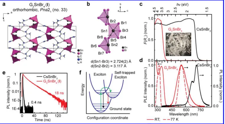
Figure 1. (a, b) Crystal structure of guanidinium tin bromide - G2SnBr4 (I). (c) Kubelka–Munk function F(R∞) = (1-R∞)2/2R∞ (R∞
-diffusive reflectance) of CsSnBr3 and I. (d) Photoluminescence (PL) and PL excitation (PLE) spectra measured on powdered crystals
of CsSnBr3 and G2SnBr4 (I). (e) Time resolved PL traces of CsSnBr3 and I at room temperature (RT). (f) A schematic of the formation
of self-trapped excitons.
maximum (FWHM) - 126 nm.7 The corresponding compound,
(C4N2H14Br)4SnBr6, containing exclusively bromide, exhibits a
QY close to 100 %.8 The structure of these compounds
comprises SnX64- octahedra isolated by organic cations. Such
emission characteristics are attributed to the emission from so-called self-trapped excitons, which are characterized by high binding energies and a low probability of interaction with intrinsic defects.26 Self-trapped excitons form due to a
combination of electronic localization of an electron-hole pair (exciton) and structural distortion that occurs fast upon photoexcitation (Figure 1f), which lead to a Jahn-Teller-like distortion in the excited state.27 Hybrid 0D main-group metal
halides are characterized by a soft lattice, strongly favoring the formation of self-trapped excitons due to facile structural distortion (exciton-phonon coupling). Radiative relaxation of self-trapped excitons leads to broad-band emission with a large Stokes shift as reported recently for a wide range of Sn(II) and Sb(III) halides.3, 6-8, 28-29 In comparison, the emission from 3D
CH3NH3SnI3 results from free-excitonic states and the PL band
is characterized by a small Stokes shift, a narrow full-width at half-maximum (FWHM), and a fast radiative lifetime.12, 30
Both organic and inorganic constituents determine the resulting crystal structure. Thus, organic cations such as formamidinium [CH(NH2)+, FA] facilitate the formation of the
3D perovskite network of FASnI3.12 However, the use of large
cations, such as phenethylammonium [C6H5(CH2)2NH3+],
typically results in a layered structure.22 A cation that is only
slightly larger than FA – guanidinium – forms a layered G2SnI4
perovskite crystal structure with corrugated Sn-I layers.31
Guanidinium is a highly symmetric molecule (D3h) and a
potential contributor of six hydrogen bonds. The G cation, due to its larger-than-FA ionic radius, destabilizes the 3D perovskite network of corner-shared Sn-X octahedra.32
Instead, GSnI3 forms a 3D network composed of Sn-I octahedra
with mixed connectivity: corner- and face-sharing.1 The
appealing attributes of the G-cation are its high thermodynamic stability, strong hydrogen bonding capabilities, and high basicity with pKa = 13.6 due to resonance stabilization by 6-8
kcal/mol.33-34 In a G-Sn-Cl system, there are two known
compounds: 1D G2SnCl4 and the 3D perovskite-like GSnCl3.35-36
Unlike G2SnI4, where the building blocks are Sn-I octahedra,
G2SnCl4 has square pyramidal Sn(II) surrounded by Cl ions. So
far, no compounds were reported in the G-Sn-Br system. Herein, we investigated the G-Sn-Br and the mixed-cation Cs-G-Sn-X (X – Br, I) systems, wherein the effect of the additional smaller cation on the obtained structure can be probed. In our study we did not succeed in obtaining quaternary mixed Cs-G-Sn(II) iodides, observing instead known ternary G2SnI41, 31 and
CsSnI3 phases.37 Therefore, the focus has been on the bromide
systems. We have synthesized G2SnBr4 (I) (Figure 1a) and
compared it to CsSnBr3, and subsequently explored mixed Cs/G
phases. G2SnBr4 is a 1D, luminescent compound with
broadband PL and a PLQY of 2 % at RT. It is thermally stable up to 300 ℃. Two layered perovskite compounds CsGSnBr4 (II)
and Cs2GSn2Br7 (III) were obtained and characterized in terms
of their crystal structure, electronic structure, and optical properties. They reveal significant quantum confinement and that the planar shape of the G cation induces significant structural and electronic anisotropy. We then compare these structural effects to those in homologous lead-based compounds.
METHODS
Chemicals, reagents and synthetic procedures. Guanidinium
carbonate (G2CO3, 99+ %), hydrobromic acid (HBr, 48 % water
solution), Sn powder (99.8 %, ~325 mesh) were purchased from Acros.
Page 2 of 11
Chemistry of Materials
1
2
3
4
5
6
7
8
9
10
11
12
13
14
15
16
17
18
19
20
21
22
23
24
25
26
27
28
29
30
31
32
33
34
35
36
37
38
39
40
41
42
43
44
45
46
47
48
49
50
51
52
53
54
55
56
57
58
Accepted
manuscritpt
Cesium bromide (CsBr, 99 %), hydroiodic acid (HI, 57% water solution stabilized with 1.5 % hypophosphorous acid, H3PO2) was obtained
from ABCR. Tin(II) bromide (SnBr2, 99.2 %) was obtained from Alfa
Aesar. All chemicals were used as received without further purification. All syntheses and further manipulations with the products were performed under inert conditions (argon or nitrogen atmosphere) using Schlenk technique. Temperatures of the syntheses, stated below, correspond to the temperatures of the glycerol bath used as a source of heat. The syntheses were conducted in 10-20 ml Schlenk vessels equipped with a stirring bar.
G2SnBr4 (I) was crystallized from HBr. Briefly, 0.250 g (2.1 mmol) of Sn powder was dissolved in 3 ml of HBr (degassed under stirring in Ar atmosphere for ~20 min beforehand); this mixture was stirred for 10 min at RT and then heated in the glycerol bath at 85-90 °C. When all Sn dissolved, 0.378 g (2.1 mmol) of G2CO3 were slowly added. A strong
evolution of gas was observed (CO2). The reaction mixture was then
stirred for an additional 5 minutes resulting in a clear colorless solution, whereupon the stirring and the heating were discontinued. Colorless transparent needles crystallized upon cooling and were separated by vacuum filtration under Ar flow. The product was dried under vacuum at 65-70 °C for 6 h. Yield - 41 % (with regard to the initial [Sn]).
CsSnBr3 was synthesized from stoichiometric quantities of Sn and CsBr precursors in HBr. Briefly, 0.180 g (1.5 mmol) of Sn were dissolved in 3-ml of HBr as described above. Next, 0.320 g (1.5 mmol) CsBr was added, and a black precipitate formed immediately. A mixture was stirred for an additional 5 min at 105 °C. Further manipulations with the product were identical to those with G2SnBr4.
Cs2GSn2Br7 (III). 0.107 g (0.9 mmol) of Sn powder was dissolved in 3 ml of HBr, stirred for 10 min at RT and then heated to 85-90 °C. When all Sn dissolved, 0.486 g (2.7 mmol) of G2CO3 and 0.1915 g (0.9 mmol)
of CsBr were slowly added. A strong evolution of gas (CO2) was
observed and a black precipitate formed. The reaction mixture was stirred and kept at 85-90 °C for about 5 minutes until a slightly yellowish solution resulted. Next, the stirring and heating were discontinued, and the mixture was cooled down under a stream of cold tap-water. Initially, some black precipitate of CsSnBr3 crystallized out
(Figure S1). In a few minutes, red crystals started appearing and the black powder re-dissolved. The mixture was left for one week for further crystallization. Finally, the red product was separated by vacuum filtration under an inert atmosphere and dried under vacuum at 65-70 °C for 6 h.
Cs8Sn6Br13I7 was crystallized from a solution of hot HI and HBr acids under N2. CsBr (0.500 g, 2.350 mmol) was first dissolved in HBr (4.0
mL) and HI (1.0 mL) solution in a 10 mL Schlenk reaction tube and sparged with N2 while stirring at RT for 30 min. SnBr2 (0.111 g, 0.399
mmol) was then added and a black precipitate formed. This mixture was then heated with a glycerol bath until an orange solution resulted (110 °C). The stirring and heating were discontinued, and the solution was cooled to RT. Within an hour orange needles crystallized out. The solution was left overnight for further crystallization. The product was separated by vacuum filtration under N2 and dried overnight under
vacuum (70-80 °C). A yield of 50.8% was estimated relative to initial [Sn].
Characterization. Powder X-ray diffraction (XRD) patterns were
collected in transmission mode (Debye-Scherrer-Geometry) with a STADI P diffractometer (STOE& Cie GmbH) equipped with a curved Ge (111)-monochromator (CuKα1 = 1.54056Å) and a silicon strip MYTHEN 1K Detector (Fa. DECTRIS). For the measurement, a ground powder was placed between an adhesive tape (for CsGSnBr4 and
Cs2GSn2Br7) or sealed in a 0.3 mm glass capillary (for G2SnBr4 and
CsSnBr3). Single-crystal XRD measurements were conducted on
Bruker Smart Platform diffractometer equipped with an Apex I CCD detector and molybdenum (MoKα = 0.71073 Å) sealed tube as an X-ray source. Crystals were tip–mounted on a micromount with paraffin oil. The data was processed with the APEX3 software package,38 and the
structure solution and refinement were performed with SHELXS39 and
SHELXL,40 respectively, which are embedded in Olex2.41 The crystal
structures were solved with direct methods, light elements (C, N) were located in the difference Fourier map, and hydrogen atoms were placed at calculated positions. The crystallographic data for the reported tin halide compounds were deposited at the Cambridge Crystallographic Data Centre (CCDC) under the codes 1854819 (G2SnBr4), 1854833
(Cs2GSn2Br7), 1854838 (CsGSnBr4), as well as at the Inorganic Crystal
Structure Database (ICSD), i.e., card number 434800 for Cs8Sn6Br13I7.
UV-Vis diffuse reflectance spectra of the microcrystalline powders
were collected using a Jasco V670 spectrophotometer equipped with deuterium (D2) lamp (190 – 350 nm) for use in UV and halogen lamp
(330 – 2700 nm) for use in UV/NIR, and an integrating sphere detector (ILN-725) with a working wavelength range of 220 – 2200 nm. The diffuse reflectance data were transformed with Kubelka-Munk model into the absorption/scattering ratio spectrum. Photoluminescence
spectra were measured with a CCD fiber spectrometer (LR1, Aseq
Instruments) with a 355 nm excitation source (frequency-tripled, picosecond Nd:YAG laser, Duetto from Time-Bandwidth). PL emission from the samples passed through a long-pass optical filter with an edge at 400 nm in order to reject the excitation laser line. PL spectra were corrected to the spectral sensitivity of the detection system. For
temperature-dependent PL measurements, a sample of CsSnBr3 was
placed atop of a 4-stage Peltier cooling/heating element in an evacuated chamber with a quartz window. The sample temperature was adjusted and stabilized with an accuracy of 0.25 °C by a home-made electronic scheme based on an Arduino microcontroller and thermocouple sensor. The current through the Peltier was reversible, thus the setup provided a wide working temperature range of -40 – 120 °C. This is an open-source project by the authors, deposited and described in details at https://www.researchgate.net/project/High- power-thermoelectric-cooler-TEC-controller-with-4-stage-Peltier-refrigerator-heater. Time-resolved photoluminescence (TR-PL) measurements were performed using a time-correlated single photon counting (TCSPC) setup, equipped with an SPC-130-EM counting module (Becker & Hickl GmbH) and an IDQ-ID-100-20-ULN avalanche photodiode (Quantique) for recording the decay traces. The average radiative lifetimes were determined as: 𝜏𝑎𝑣𝑔=
∑2𝑖=1𝜏𝑖2∙𝐴𝑖
∑2𝑖=1𝜏𝑖∙𝐴𝑖
, where Ai and τi are the corresponding amplitudes and exponential decay parameters in the biexponential analysis. For measurements of PL and PLE spectra at low temperature (77 K), the sample was encapsulated in a quartz tube filled with Ar gas and placed in a homemade cryostat. Low temperature (77 K) and RT absolute PLQY were measured with excitation at 340 nm using Quantaurus-QY spectrometer from Hamamatsu. The sample was encapsulated in a quartz tube filled with Ar gas. PL measurements at lower temperatures (in the case of Cs2GSn2Br7), down to 5 K, were conducted in a helium cryostat and PL
spectroscopy was performed by exciting the sample with a frequency-doubled Ti:Sapphire mode-locked laser delivering pulses of about 150 fs duration at 400 nm and a repetition rate of 80 MHz. The time-integrated PL was analyzed using a CCD-coupled grating spectrometer, whereas TR-PL traces were recorded with a streak camera. Thermal
analysis [thermogravimetry (TG) and differential scanning
calorimetry (DSC)] was performed using a Netzsch Simultaneous Thermal Analyzer (STA 449 F5 Jupiter). A powdered sample of G2SnBr4
(21.9 mg) was placed in an alumina crucible (without a lid) and heated under Ar gas flow (50 ml/min) to 850 ℃ (10 °C min-1). Scanning
electron microscopy (SEM) was carried out on a Quanta 200F
microscope (Thermo Fisher Scientific) operated at an acceleration voltage of 20 kV.
1
2
3
4
5
6
7
8
9
10
11
12
13
14
15
16
17
18
19
20
21
22
23
24
25
26
27
28
29
30
31
32
33
34
35
36
37
38
39
40
41
42
43
44
45
46
47
48
49
50
51
52
53
54
55
56
57
Accepted
manuscritpt
Figure 2. (a) Electronic band diagram of G2SnBr4 (I) computed by DFT. No dispersion can be observed except in the direction of the
1D chains [010] (Γ➝Y, R➝U, and Z➝T paths). The space group Pna21 is a polar space group. Therefore, a Rashba splitting of the
band edge states is predicted both in the conduction and valence bands away from the Y, R and T critical points of the Brillouin zone. (b) Representation of the electronic densities of the conduction (red) and valence (blue) edge states.
Energy-dispersive X-ray spectroscopy (EDXS) was performed with
an Octane SDD detector (EDAX, Ametec) attached to the microscope column. For spectra recording and quantification (ZAF correction), the software Gemini (EDAX) was used.
Computational details. First-principles calculations were performed
with experimental crystal structures using density functional theory (DFT) as implemented in the SIESTA package.42-43 Calculations have
been carried out on experimental structures with the GGA functional in the PBE form.44 Core electrons were described with Troullier-Martins
pseudopotentials,45 while valence wavefunctions were developed over
double-ζ polarized basis set of finite-range numerical pseudoatomic orbitals.46 Spin-orbit coupling was taken into account through the
on-site approximation as proposed by Fernández-Seivane et al..47 In all
cases, an energy cutoff of 150 Ry for real-space mesh size was used.
RESULTS AND DISCUSSION
All presented compounds were crystallized from hydrobromic acid (HBr, 48 % water solution) under Argon atmosphere using Sn powder, CsBr, and G2CO3 as precursors. G2SnBr4 (I),
obtained from stoichiometric quantities of G and Sn(II), crystallizes as colorless transparent needles. Compound I was then characterized by single-crystal XRD (Figures 1a, b, S2, Table S1-S4) and found to crystallize in the orthorhombic crystal system, space group Pna21. This structure consists of
corrugated chains oriented along [010] (i.e., extended in b direction), comprising corner-sharing square pyramids - [SnBr5]2-. The formation of such pyramids emphasizes the
stereoactivity of the lone pair of Sn(II). The G cations are situated in the space between the chains and connect them via hydrogen-halogen bonds into a 3D supramolecular structure (Table S2). Two non-equivalent pyramids can be identified, which connect in an alternating manner. In both kinds of pyramids, Sn atoms are displaced out of the basal planes (by 0.23 and 0.24 Å, for Br1Br2Br5Br4 and Br2Br5Br8Br7 planes, respectively, Figure 1b). The Sn-Br bond lengths are in the range of 2.724(2)–3.117 Å, which is comparable to the
distances found in (NH4)SnBr3×H2O (2.623-3.047 Å), where
Sn(II) has the same square-pyramidal coordination.48 The
shortest Sn-Br bond is with the Br ion at the apex of the pyramid. G2SnBr4 (I) has a similar crystal structure as G2PbBr4,
which contains an alternating orientation of [PbBr5]2- square
pyramids in 1D chains.49 The 1D character is confirmed by
inspection of the DFT electronic structure (Figure 2). Indeed, the band diagram (Figure 2a) exhibits an indirect bandgap of 3.12 eV, and no dispersion of the edge state bands is observed except when following a path corresponding to the [010] crystal direction. Furthermore, the computed electronic edge state densities exhibit sizeable overlaps, but only along the b crystallographic direction (Figure 2b) thus confirming the 1D character of the density of states close to the bandgap. It is also worth noticing that a Rashba splitting of the band edge states is observed both in the conduction and valence bands away from the Y, R and T critical points of the Brillouin zone as a result of the polar space group Pna21 assigned to (I). Sn-I
square pyramidal units were also observed when using larger cations, such as [C3H7N(C2H4)3NC3H7]2+.19 G2SnBr4 (I) is
thermally stable up to at least 300 °C (see TGA/DSC analysis in Figure S3). Two endothermic processes without mass loss occur before the decomposition at around 146 and 190 °C and indicate melting and/or other structural transitions.
Studies on a ternary 3D phase – the black CsSnBr3 – date back
to as early as the 1970s. CsSnBr3 crystallizes in a cubic
perovskite crystal structure (space group Pm-3m, Figure 3a) and melts congruently at 450 °C.50-52 A phase transition to a
tetragonally distorted lattice appears upon cooling to below 19 °C.52 The yellow CsSnI3 crystallizes in the orthorhombic crystal
system. CsSnI3 is a 1D compound composed of edge-sharing
[SnI6]-1 octahedra,53 and converts into a cubic 3D phase only at
152 °C.52 Similarly, CsPbI3 is known to crystallize in a 3D-lattice
(cubic, space group Pm-3m) at higher temperatures and
Page 4 of 11
Chemistry of Materials
1
2
3
4
5
6
7
8
9
10
11
12
13
14
15
16
17
18
19
20
21
22
23
24
25
26
27
28
29
30
31
32
33
34
35
36
37
38
39
40
41
42
43
44
45
46
47
48
49
50
51
52
53
54
55
56
57
58
Accepted
manuscritpt
Figure 3. (a) Crystal structure of cubic 3D-perovskite CsSnBr3. (b, c) Crystal structure of two-dimensional perovskites: CsGSnBr4 (II)
and Cs2GSn2Br7 (III). (d) Kubelka–Munk function of CsSnBr3 and III at RT. (e) Selected low-temperature PL spectra of III. (f) Selected
low-temperature time-resolved PL spectra of III.
converts into 1D-phase, analogous to 1D-CsSnI3, within the 329
- 290 °C temperature range.54
We were then interested to see the effect of Br-I mixing in the Cs-Sn-X system. Interestingly, the addition of iodide with [I]/[Sn] = 19/1 (in concentrated HBr) leads to the precipitation of Cs8Sn6Br13I7 in the form of orange needles. It crystallizes in
the orthorhombic crystal system, space group Cmcm (Tables S5-S7) and consists of layers of corner (through μ2-Br) and
edge-sharing (through μ3-I ions) distorted [SnBr4I2]-1⅔ and
[SnBr3I3]-1⅙octahedra (Figure S4a, b). Iodide has one full and
two partially occupied positions that are shared with bromide ions. The Cs+ cations are situated in-between, as well as within,
Sn(II) halide layers. There are two types of crystallographic surroundings for the Sn(II) ions; one characterized by the presense of a very weak Sn-I bond of 3.723 Å – in [SnBr3I3]-1⅙
octahedra (see Sn1 atom in Figure S4b). The Sn2-I1 distances within [SnBr4I2]-1⅔ are 3.454 Å, which is in the range of d(Sn-I)
in CsSnI3, 2.942 – 3.470 Å.53 Based on powder XRD analysis,
Cs8Sn6Br13I7 was obtained as a pure phase (Figure S4c) with a
homogeneous composition that was estimated with EDX (Figure S5a-c). The same structural motif was found in Cs2.38Rb1.62Sn3Cl8I2, recently reported by Li, et al.,55 obtained by
solid-state reaction. The optical band edge of Cs8Sn6Br13I7 lies
at 2.23 eV (Figure S6a, b), which is 0.58 eV smaller than the optical bandgap of Cs2.38Rb1.62Sn3Cl8I2.55
By comparing the experimental powder XRD patterns with those simulated from single-crystal XRD data obtained herein (except for CsSnBr3, where ICSD card 4071 was used), I and
CsSnBr3 were determined to be phase-pure (Figure S7, S8).
CsSnBr3 also appears to contain amorphous CsSnBr3 (Figure
S8), which can explain the partially-resolved component at 650-700 nm in the PL spectrum (Figure 1d). We then obtained two mixed guanidinium-cesium tin bromides: CsGSnBr4 (II,
orange colored) and Cs2GSn2Br7 (III, red-colored), as a mixture
of crystals. Both compounds are layered perovskites (Figure 3b, c). The formation of these phases was found to be in strong competition with the crystallization of compounds I and CsSnBr3. Cs2GSn2Br7 (III) was obtained as the dominant phase,
with CsGSnBr4 (II) as a major impurity (below 10 %, Figure S9)
at a molar ratio of Cs/G/Sn = 1/6/1. Optical absorption analysis of the sample of Cs2GSn2Br7 by a Kubelka-Munk function points
to a possible trace quantity of a rather amorphous CsSnBr3 thus
giving rise to a small shoulder in the 650-700 nm region (Figure 3d). Both II and III crystallize in the orthorhombic crystal system, namely in Imma (II) and Cmmm (III) space groups, respectively (Figure 3b, c, Table S1). The crystal structures of
II and III consist of 2D perovskite layers of corner-sharing
[SnBr6]4- octahedra that are separated by cesium and
guanidinium cations. The derivation of these structures can be visualized by cutting the parental cubic CsSnBr3 perovskite
lattice along the (100) crystallographic plane and adding the octahedral tilting (discussed later in detail). The importance of the mixed-cation design for obtaining 2D-perovskites had been previously reported for the analogous CsGPbBr(I)4 and
Cs2GPb2Br7 compounds.49 Compound II contains monolayers
of corner-sharing octahedra (Figure 3b), whereas compound
III features double layers, connected via corners (Figure 3c). To
the best of our knowledge, this is the first tin bromide featuring multi-layers. The perovskite slabs are mutually shifted in-plane by a vector a/2 (a being an ideal cubic cell vector, Figure 3c). Cs+ and G
1
2
3
4
5
6
7
8
9
10
11
12
13
14
15
16
17
18
19
20
21
22
23
24
25
26
27
28
29
30
31
32
33
34
35
36
37
38
39
40
41
42
43
44
45
46
47
48
49
50
51
52
53
54
55
56
57
Accepted
manuscritpt
Figure 4. (a) Electronic band structure and (b) representation of the electronic densities of the conduction (red) and valence (blue)
edge states (at the R point of the Imma Brillouin zone) of CsGSnBr4 (II). R➝E0 corresponds to the stacking direction. (b) and (d),
same for Cs2GSn2Br7 (III). S➝J2 corresponds to the stacking direction. (e) Electronic band structures of CsGPbBr4 and (f) Cs2GPb2Br7.
Electron densities are computed at the R point for II (b) and S point for III (d). cations in II and III are both situated in the interlayer space,
and alternate with each other in a periodic manner. In Cs2GSn2Br7 (III), cesium cations also fill the voids within the
perovskite layers. G forms hydrogen bonds with the bromide ions from the perovskite layers (Table S8, S9). G cations are closely packed with intermolecular d(C···N) distance of ca. 3 Å. Due to the difference in ionic radii of the Cs+ and G cations and
the planar shape of the latter, Sn-Br octahedra are tilted in an alternating manner along the crystallographic axis b and c for
II (Figure 3b) and III (Figure 3c left), respectively. This
generates smaller cavities for Cs+ and large voids for G cations.
However, in the in-plane direction (for instance along the crystallographic axis a for III, Figure 3c right) the planar shape of the G cation and small atomic radius of Cs+ lead to the
absence of steric strain with almost perfectly collinear Sn and Br atoms and subsequently longer Sn-Sn distances (6.011 and 5.965 Å for II and III, respectively). This might contribute to an observed disorder in atomic positions of bromide along this direction. In CsGSnBr4 (II), d(Sn-Br) = 2.909(2)-3.006(1) Å, are
comparable to Sn-Br distances in a CsSnBr3 cubic phase
[d(Sn-Br) = 2.898 Å].50 Sn-Br-Sn angles are in the range of
155.9(5)-180.0° (Figure S10). CsGSnBr4 and CsGPbBr4 both crystallize in
the space group Imma, and are isotypic.49 III is isotypic to
Cs2GPb2Br7,and crystallizes in the space group Cmmm.49 The
average Sn-Br distances for III are in the range of 2.915-2.987(1) Å (for additional crystallographic data for II and III, see Tables S10-S13).The interlayer Br···Br distances along the stacking direction (c and b for II and III, respectively) are rather short: d(Br···Br) = 4.161 Å in CsGPbBr4 (II) and
d(Br···Br) = 4.070 Å in Cs2GSn2Br7 (III).
In 3D perovskites, the critical point of the Brillouin zone where a direct bandgap is observed is either the R-point,56 for
the cubic Pm-3m phase, or the Z-point for the distorted tetragonal P4/mbm phase (Figure S11). In both cases, the critical wavevectors have the point symmetries of their respective lattices (m-3m and 4/mmm). Similar symmetry considerations lead to critical wavevectors located along the stacking directions at the X (0,0,1) and Y (0,1,0) high-symmetry points for II and III, respectively, in the Imma and Cmmm Brillouin zones (both with point groups mmm). However, DFT simulations (Figure 4a and c) show that the electronic bandgaps are predicted to be direct at the R (0.5,0,0.5) and S (0.5,0.5,0) points of the Brillouin zones of II and III, respectively. In both cases, the point symmetry of the critical wavevector is reduced from mmm to 2/m. This can be related to the anisotropy of the out-of-plane octahedral tilts, which is directly induced by the shape of the G cations. The octahedral tilting is clearly apparent only in the (b,c) crystallographic planes (Figure 3-b and c). The difference between II and III lies in the fact that the (b,c) plane contains the stacking axis along c for II and along b for III. Furthermore, due to lattice distortions, the periodicity of the electronic density is doubled along b (c) for II (III), in contrast to the a direction. In turn, the valence band maxima and the conduction band minima show different hybridizations along all three directions (Figure 4b, 4d, and Figure S12) as well as different band dispersions (Figure 4a and c). Both compounds II and III exhibit flat dispersions along the stacking axis despite the short Br-Br distances, a characteristic feature of 2D systems. Analogously to CsSnBr3
(Figure S11) and contrary to I (Figure 2), the bandgap remains
Page 6 of 11
Chemistry of Materials
1
2
3
4
5
6
7
8
9
10
11
12
13
14
15
16
17
18
19
20
21
22
23
24
25
26
27
28
29
30
31
32
33
34
35
36
37
38
39
40
41
42
43
44
45
46
47
48
49
50
51
52
53
54
55
56
57
58
Accepted
manuscritpt
7
direct in both II and III (Figure 4a and c) with a systematic decrease of the bandgap values with the decrease of dimensionality and thickness of perovskite layers. These variations in DFT bandgap energies (Table S14) are related to the equivalent quantum well thickness (n = 1, 2 or ), which is roughly doubled when going from CsGSnBr4 (II) to Cs2GSn2Br7
(III) as a result of quantum confinement.
To experimentally probe the energy bandgaps in these hybrid tin bromide compounds, an optical absorption analysis by means of a Kubelka-Munk function as well as PL measurements were performed (Figure 1c,d, 3d,e). The Kubelka-Munk absorption representation was derived from the diffuse reflectance spectra of powdered samples, and was estimated as
F(R∞) = α/S = (1−R∞)2/2R∞ [F(R∞) - Kubelka-Munk units, α -
absorption coefficient, S - the scattering coefficient, and R∞ - the
reflectance of an infinitely thick layer]. Here we neglected the influence of excitonic effects on the absorption, because the excitonic band cannot be consistently resolved for all compounds and thus correctly de-convoluted from the bandgap absorption edge. Hence the bandgap can be slightly underestimated. The optical bandgap energies for I, III and CsSnBr3 were determined by plotting [F(R∞)·hν]r versus (hν)
(hν - the incident photon energy, r = 2 for direct bandgap semiconductor, and r = 1/2 for indirect bandgap semiconductor; Figure S13a,b). The highest absorption edge energy (ca. 3.11 eV) was found for G2SnBr4 (I) (Figure 1c),
which is in agreement with its lowest electronic dimensionality (1D). The 3D cubic CsSnBr3 has the smallest bandgap energy
(1.74 eV, in agreement with literature57), whereas the 2D
Cs2GSn2Br7 (III) has an intermediate bandgap value of 2.16 eV
(Figure 3d). Compound II could not be obtained in the phase-pure form needed for diffuse reflectance (only individual small crystallites could be selected for a single-crystal XRD analysis). However, the visual appearance of II pointed towards an expected higher bandgap in comparison to III (orange vs. red). Despite the well-known underestimation of bandgaps, such a decrease is predicted from DFT calculations (Figure 4 and Table S14) with 1.04 eV for II and 0.84 eV III. Cs2GPb2Br7 has a
larger optical experimental bandgap than III, by 0.44 eV (2.60 eV vs. 2.16 eV).49 A similar scenario was observed for the pair
of (C6H9C2H4NH3)2SnBr4 (2.5 eV optical bandgap) and its lead
analog (2.9 eV).58 This might be a result of the difference in the
E3 ionization energies between tin and lead [E3(Pb) = 31.94 eV
and E3(Sn) = 30.5 eV], the effect of the additional polarizability
(presence of filled diffuse d and f orbitals below the valence electrons in Pb), and the distortions of the M-X (M = Sn, Pb) octahedra. A different degree of tilting of the MBr6 octahedra is
observed for Cs2GPb2Br7 and III (Figure S14), with stronger
deviations from the ideal 180° for the lead compound. Interestingly, despite the different tilts of the octahedra, the angles are at the end compensated in a manner that gives the required amount of space for guanidinium and cesium cations. Figure 4e and f report the computed band structures for the lead-based analogs of compounds II and III that share many similarities with the tin-based layered perovskites (Figure 4a and c). Both for II and III, the predicted electronic bandgaps follow the same trends as the above mentioned experimental results. For instance, the bandgap increases from 1.04 eV (Sn) to 1.55 eV (Pb) for II and from 0.84 eV (Sn) to 1.32 eV (Pb) for
III.
Both CsSnBr3 and I are luminescent at RT, unlike II and III. The
PL of G2SnBr4 (I) at RT is characterized by a broad emission
band (Figure 1d) with a FWHM of ca. 121 nm, 2 % PLQY, and a large Stokes shift of ca. 208 nm. At 77 K, the PLQY reaches 75±5 % and the PL band narrows (FWHM ~72 nm) while retaining the same peak position at 557 nm with a Stokes shift of 233 nm. Additionally, the PL excitation spectrum at 77 K is blue-shifted compared to that at RT. CsSnBr3 exhibits a PL maximum at 1.70
eV (Figure 1d) at RT, which is consistent with the literature value.57 In the PL spectrum of CsSnBr3, a shoulder was
observed at the higher energy side, which seems to originate from an amorphous or nanocrystalline CsSnBr3 impurity.59 A
blue shift of the emission bands of CsSnBr3 was observed when
the temperature increased from 228 to 383 K (Figure S15). This trend is consistent with previous temperature-dependent PL theoretical and experimental studies and is explained by the lattice expansion upon heating and local displacements of the Sn(II) cation.57, 60-61 Large differences in the width of the PL
bands and Stokes shifts for G2SnBr4 (I) and CsSnBr3 indicate
different radiative processes in these compounds. Time-resolved PL measurements (Figure 1e) yielded a PL lifetime of 0.4 ns for CsSnBr3 and 18 ns in compound I. The short lifetime,
the small Stokes shift and the narrow PL band attest to the excitonic nature of the radiative transition in CsSnBr3. On the
contrary, the longer PL lifetime and larger Stokes shift and broader FWHM point to emission via self-trapped excitons in compound I (Figure 1f). Importantly, the PL lifetime in 1D G2SnBr4 is much faster (18 ns) than that commonly found in 0D
Sn(II)-halides (102-103 ns for bromide) at RT.6-8, 28 This might
eventually lead to a practical advantage, for instance, in the context of applications such as white-light sources,7-8, 27 as the
achievable saturated emission brightness scales with the PL lifetime.
For II and III, which are structurally more rigid and exhibit a delocalized electronic structure that reduces the propensity to form self-trapped excitons, the PL was measurable only at cryogenic temperatures (5 K - 120 K, Figure 3e). At 5 K, the main band peaks at 517 nm with an additional emission band around 577 nm. A broad emission band above 700 nm is also visible. Due to the very low PLQY and presence of different phases within the same sample, it is difficult to draw solid conclusions. Yet one can attribute the main emission bands to free excitons or self-trapped excitons with low stabilization energy (due to hindered structural distortion as compared to 0D and 1D-compounds). Finally, the lowest energy band might stem from surface defects. By increasing the temperature, the PL intensity quickly drops due to the activation of non-radiative processes. We have performed time-resolved PL measurements with a streak camera system, and the results are displayed in Figure 3f. The measured sub-100-ps decay times and their dependence on temperature attest to the presence of non-radiative processes, which efficiently quench radiative recombination.
In conclusion, we presented a highly luminescent at 77 K 1D-compound G2SnBr4, as well as layered 2D-perovskites
CsGSnBr4 and Cs2GSn2Br7. In G2SnBr4, the Sn(II) lone pair is
stereoactive and influences the coordination environment of Sn(II). G2SnBr4 is a luminescent compound with broadband
emission from self-trapped excitonic states that are enabled by the soft-lattice and electronic localization. This emission is characterized by PL QY of 2 % at RT and 75±5 % at 77 K. G2SnBr4 does not thermally decompose until 300 ℃. The
addition of cesium to the G-Sn-Br system promotes the formation of structurally more rigid, layered perovskite compounds, obscuring the formation of self-trapped excitons
1
2
3
4
5
6
7
8
9
10
11
12
13
14
15
16
17
18
19
20
21
22
23
24
25
26
27
28
29
30
31
32
33
34
35
36
37
38
39
40
41
42
43
44
45
46
47
48
49
50
51
52
53
54
55
56
57
Accepted
manuscritpt
8
but leading to a delocalized electronic structure. Cs2GSn2Br7
has a smaller bandgap than its lead analog, Cs2GPb2Br7, due to
the difference in E3 ionization energies of tin and lead, higher
electronegativity of Pb, as well as the different degree of structural distortion. Lastly, in-plane electronic coupling is anisotropic as a result of the planar shape of the guanidinium cation, which leads to significant octahedral out-of-plane tilting in only one of the two directions.
ASSOCIATED CONTENT
Supporting Information
The Supporting Information is available free of charge on the ACS Publications website. The Supporting information contains additional data on single crystal and powder XRD, thermal analysis, optical characterization, as well as EDX spectroscopy and electronic structure calculations.
AUTHOR INFORMATION
Corresponding Author
*mvkovalenko@ethz.ch
Notes
The authors declare no competing financial interests. ACKNOWLEDGMENT
Authors thank IBM-Zurich Research, in particular Dr. T. Stöferle and Dr. R.F. Mahrt, for support with low-temperature PL experiments. This work was financially supported by the European Union through the FP7 (ERC Starting Grant NANOSOLID, GA No. 306733). DFT calculations were performed at the Institut des Sciences Chimiques de Rennes, which received funding from Agence Nationale pour la Recherche (TRANSHYPERO project) and the work was granted access to the HPC resources of TGCC/CINES/IDRIS under the allocation 2018-A0030907682 made by GENCI. J.E. is a senior member of Institut Universitaire de France. The work at Institut FOTON was supported by Agence Nationale pour la Recherche (SupersansPlomb project).
REFERENCES
1. Stoumpos, C. C.; Mao, L.; Malliakas, C. D.; Kanatzidis, M. G., Structure–band gap relationships in hexagonal polytypes and low-dimensional structures of hybrid tin iodide perovskites. Inorg. Chem. 2017, 56 (1), 56-73.
2. Xu, Z.; Mitzi, D. B., SnI42--based hybrid perovskites templated by multiple organic cations: combining organic functionalities through noncovalent interactions. Chem. Mater. 2003, 15 (19), 3632-3637. 3. Zhou, C.; Tian, Y.; Wang, M.; Rose, A.; Besara, T.; Doyle Nicholas, K.; Yuan, Z.; Wang Jamie, C.; Clark, R.; Hu, Y.; Siegrist, T.; Lin, S.; Ma, B., Low‐dimensional organic tin bromide perovskites and their photoinduced structural
transformation. Angew. Chem. Int. Ed. 2017, 56 (31), 9018-9022.
4. Herrmann, H.; Walter, P.; Kaifer, E.; Himmel, H. J., Incorporation of a redox‐active bis(guanidine) in low‐ dimensional tin and lead iodide structures. Eur. J. Inorg. Chem. 2017, 2017 (47), 5539-5544.
5. Lode, C.; Krautscheid, H., Schwache Sn…I‐ wechselwirkungen in den kristallstrukturen der iodostannate [SnI4]2– und [SnI3]–. Z. Anorg. Allg. Chem.
2000, 626 (2), 326-331.
6. Zhou, C.; Lin, H.; Shi, H.; Tian, Y.; Pak, C.; Shatruk, M.; Zhou, Y.; Djurovich, P.; Du, M. H.; Ma, B., A zero‐ dimensional organic seesaw‐shaped tin bromide with highly efficient strongly stokes‐shifted deep‐red emission. Angew. Chem. Int. Ed. 2017, 57 (4), 1021-1024. 7. Zhou, C.; Tian, Y.; Yuan, Z.; Lin, H.; Chen, B.; Clark, R.; Dilbeck, T.; Zhou, Y.; Hurley, J.; Neu, J.; Besara, T.; Siegrist, T.; Djurovich, P.; Ma, B., Highly efficient broadband yellow phosphor based on zero-dimensional tin mixed-halide perovskite. ACS Appl. Mater. Interfaces
2017, 9 (51), 44579-44583.
8. Zhou, C.; Lin, H.; Tian, Y.; Yuan, Z.; Clark, R.; Chen, B.; van de Burgt, L. J.; Wang, J. C.; Zhou, Y.; Hanson, K.; Meisner, Q. J.; Neu, J.; Besara, T.; Siegrist, T.; Lambers, E.; Djurovich, P.; Ma, B., Luminescent zero-dimensional organic metal halide hybrids with near-unity quantum efficiency. Chem. Sci. 2018, 9 (3), 586-593.
9. Hao, F.; Stoumpos, C. C.; Guo, P.; Zhou, N.; Marks, T. J.; Chang, R. P. H.; Kanatzidis, M. G., Solvent-mediated crystallization of CH3NHSnI3 films for heterojunction depleted perovskite solar cells. J. Am. Chem. Soc. 2015, 137 (35), 11445-11452.
10. Noel, N. K.; Stranks, S. D.; Abate, A.; Wehrenfennig, C.; Guarnera, S.; Haghighirad, A.-A.; Sadhanala, A.; Eperon, G. E.; Pathak, S. K.; Johnston, M. B.; Petrozza, A.; Herz, L. M.; Snaith, H. J., Lead-free organic-inorganic tin halide perovskites for photovoltaic applications. Energy Environ. Sci. 2014, 7 (9), 3061-3068.
11. Lu, Z. H.; Zhifu, L.; Zhengbao, H.; Kit, N. W.; Jian, M.; Sing, W. K.; Wan‐Jian, Y.; H., C. W. C., Low‐bandgap methylammonium‐rubidium cation Sn‐rich perovskites for efficient ultraviolet–visible–near infrared photodetectors. Adv. Funct. Mater. 2018, 28 (16), 1706068.
12. Stoumpos, C. C.; Malliakas, C. D.; Kanatzidis, M. G., Semiconducting tin and lead iodide perovskites with organic cations: phase transitions, high mobilities, and near-infrared photoluminescent properties. Inorg. Chem.
2013, 52 (15), 9019-9038.
13. Mitzi, D. B.; Wang, S.; Feild, C. A.; Chess, C. A.; Guloy, A. M., Conducting layered organic-inorganic halides containing <110>-oriented perovskite sheets. Science 1995, 267 (5203), 1473-1476.
14. Guan, J.; Tang, Z.; M. Guloy, A., α-[NH3(CH2)5NH3]SnI4: a new layered perovskite structure.
Chem. Comm. 1999, (18), 1833-1834.
Page 8 of 11
Chemistry of Materials
1
2
3
4
5
6
7
8
9
10
11
12
13
14
15
16
17
18
19
20
21
22
23
24
25
26
27
28
29
30
31
32
33
34
35
36
37
38
39
40
41
42
43
44
45
46
47
48
49
50
51
52
53
54
55
56
57
58
Accepted
manuscritpt
9
15. Yamada, K.; Kuranaga, Y.; Ueda, K.; Goto, S.;Okuda, T.; Furukawa, Y., Phase transition and electric conductivity of ASnCl3 (A = Cs and CH3NH3). Bull. Chem.
Soc. Jpn. 1998, 71 (1), 127-134.
16. Yamada, K.; Nakada, K.; Takeuchi, Y.; Nawa, K.; Yamane, Y., Tunable perovskite semiconductor CH3NH3SnX3 (X: Cl, Br, or I) characterized by X-ray and DTA. Bull. Chem. Soc. Jpn. 2011, 84 (9), 926-932.
17. Dang, Y.; Zhong, C.; Zhang, G.; Ju, D.; Wang, L.; Xia, S.; Xia, H.; Tao, X., Crystallographic investigations into properties of acentric hybrid perovskite single crystals NH(CH3)3SnX3 (X = Cl, Br). Chem. Mater. 2016, 28 (19), 6968-6974.
18. Chouaib, H.; Kamoun, S.; Costa, L. C.; Graça, M. P. F., Synthesis, crystal structure and electrical properties of N,N-dimethylanilinium trichloridostannate (II): (C8H12N)SnCl3. J. Mol. Struct. 2015, 1102, 71-80.
19. Lode, C.; Krautscheid, H.; Müller, U., [C3H7N(C2H4)3NC3H7]2 ∞1[Sn4I12] ‐ ein iodostannat aus verknüpften SnI5‐pyramiden. Z. Anorg. Allg. Chem. 2005,
631 (2‐3), 587-591.
20. Raptopoulou, C. P.; Terzis, A.; Mousdis, G. A.; Papavassiliou, G. C., Preparation, structure and optical properties of [CH3SC(NH2)2]3SnI5, [CH3SC(NH2)2][HSC(NH2)2]SnBr4, (CH3C5H4NCH3)PbBr3, and [C6H5CH2SC(NH2)2]4Pb3I10. Z. Naturforsch. B Chem.
2002, 57 (6), 645.
21. Knutson, J. L.; Martin, J. D.; Mitzi, D. B., Tuning the band gap in hybrid tin iodide perovskite semiconductors using structural templating. Inorg. Chem. 2005, 44 (13), 4699-4705.
22. Papavassiliou, G. C.; Koutselas, I. B.; Terzis, A.; Whangbo, M. H., Structural and electronic properties of
the natural quantum-well system
(C6H5CH2CH2NH3)2SnI4. Solid State Commun. 1994, 91 (9), 695-698.
23. Xu, Z.; Mitzi, D. B.; Dimitrakopoulos, C. D.; Maxcy,
K. R., Semiconducting perovskites
(2-XC6H4C2H4NH3)2SnI4 (X = F, Cl, Br): steric interaction between the organic and inorganic layers. Inorg. Chem.
2003, 42 (6), 2031-2039.
24. Xu, Z.; Mitzi, D. B., SnI42--based hybrid perovskites templated by multiple organic cations: combining organic functionalities through noncovalent interactions. Chem. Mater. 2003, 15 (19), 3632-3637. 25. Lanzetta, L.; Marin-Beloqui, J. M.; Sanchez-Molina, I.; Ding, D.; Haque, S. A., Two-dimensional organic tin halide perovskites with tunable visible emission and their use in light-emitting devices. ACS Energy Lett. 2017, 2 (7), 1662-1668.
26. Han, D.; Shi, H.; Ming, W.; Zhou, C.; Ma, B.; Saparov, B.; Ma, Y.; Chen, S.; Du, M. H., Unraveling luminescence mechanisms in zero-dimensional halide perovskites. J. Mater. Chem. C 2018, 6 (24), 6398-6405 27. Luo, J.; Wang, X.; Li, S.; Liu, J.; Guo, Y.; Niu, G.; Yao, L.; Fu, Y.; Gao, L.; Dong, Q.; Zhao, C.; Leng, M.; Ma, F.; Liang, W.; Wang, L.; Jin, S.; Han, J.; Zhang, L.; Etheridge, J.; Wang,
J.; Yan, Y.; Sargent, E. H.; Tang, J., Efficient and stable emission of warm-white light from lead-free halide double perovskites. Nature 2018, 563 (7732), 541-545. 28. Benin, B. M.; Dirin, D. N.; Morad, V.; Wörle, M.; Yakunin, S.; Rainò, G.; Nazarenko, O.; Fischer, M.; Infante, I.; Kovalenko, M. V., Highly emissive self-trapped excitons in fully inorganic zero-dimensional tin halides. Angew. Chem., Int. Ed. 2018, 57 (35), 11329-11333. 29. Zhou, C.; Worku, M.; Neu, J.; Lin, H.; Tian, Y.; Lee, S.; Zhou, Y.; Han, D.; Chen, S.; Hao, A.; Djurovich, P. I.; Siegrist, T.; Du, M.-H.; Ma, B., Facile preparation of light emitting organic metal halide crystals with near-unity quantum efficiency. Chem. Mater. 2018, 30 (7), 2374-2378.
30. Parrott, E. S.; Milot, R. L.; Stergiopoulos, T.; Snaith, H. J.; Johnston, M. B.; Herz, L. M., Effect of structural phase transition on charge-carrier lifetimes and defects in CH3NH3SnI3 Perovskite. J. Phys. Chem. Lett.
2016, 7 (7), 1321-1326.
31. Hillebrecht, H.; Daub, M.; Haber, C., Synthesis, crystal structures, optical properties and phase transitions of the layered guanidinium-based hybrid perovskites (C(NH2)3)2MI4; M = Sn, Pb. Eur. J. Inorg. Chem.
2016, 2017 (7), 1120-1126.
32. Kieslich, G.; Sun, S.; Cheetham, A. K., An extended Tolerance Factor approach for organic–inorganic perovskites. Chem. Sci. 2015, 6 (6), 3430-3433.
33. Pauling, L., The nature of the chemical bond and the structure of molecules and crystals. Cornell University Press: Ithaca, New York 1940, 286-288.
34. Russell, V. A.; Ward, M. D., Molecular crystals with dimensionally controlled hydrogen-bonded nanostructures. Chem. Mater. 1996, 8, 1654-1666. 35. Szafrański, M.; Ståhl, K., Pressure-induced decoupling of the order-disorder and displacive contributions to the phase transition in diguanidinium tetrachlorostannate. Phys. Rev. B 2000, 62 (13), 8787-8793.
36. Szafrański, M.; Ståhl, K., Crystal structure and phase transitions in perovskite-like C(NH2)3SnCl3. J. Solid
State Chem. 2007, 180 (8), 2209-2215.
37. Yamada, K.; Funabiki, S.; Horimoto, H.; Matsui, T.; Okuda, T.; Ichiba, S., Structural phase transitions of the polymorphs of CsSnI3 by means of rietveld analysis of the X-ray diffraction. Chem. Lett. 1991, 20 (5), 801-804.
38. Brucker APEX3 v2017.3-0. Bruker AXS Inc., Madison, Wisconsin, USA, 2016.
39. Sheldrick, G., A short history of SHELX. Acta Crystallogr. A 2008, 64 (1), 112-122.
40. Sheldrick, G., Crystal structure refinement with SHELXL. Acta Crystallogr. C 2015, 71 (1), 3-8.
41. Dolomanov, O. V.; Bourhis, L. J.; Gildea, R. J.; Howard, J. A. K.; Puschmann, H., OLEX2: a complete structure solution, refinement and analysis program. J. Appl. Crystallogr. 2009, 42 (2), 339-341.
1
2
3
4
5
6
7
8
9
10
11
12
13
14
15
16
17
18
19
20
21
22
23
24
25
26
27
28
29
30
31
32
33
34
35
36
37
38
39
40
41
42
43
44
45
46
47
48
49
50
51
52
53
54
55
56
57
Accepted
manuscritpt
10
42. Soler, J. M.; Artacho, E.; Gale, J. D.; García, A.;Junquera, J.; Ordejón, P.; Sánchez-Portal, D., The SIESTA method for ab initio order- N materials simulation. J. Phys. Condens. Matter. 2002, 14 (11), 2745.
43. Artacho, E.; Anglada, E.; Diéguez, O.; Gale, J. D.; García, A.; Junquera, J.; Martin, J. D.; Ordejón, P.; Pruneda, J. M.; Sánchez-Portal, D.; Soler, J. M., The SIESTA method; developments and applicability. J. Phys. Condens. Matter.
2008, 20 (6), 064208.
44. Perdew, J. P.; Burke, K.; Ernzerhof, M., Generalized gradient approximation made simple. Phys. Rev. Lett. 1996, 77 (18), 3865-3868.
45. Troullier, N.; Martins, J. L., Efficient pseudopotentials for plane-wave calculations. Phys. Rev. B 1991, 43 (3), 1993-2006.
46. Artacho, E.; Sánchez‐Portal, D.; Ordejón, P.; García, A.; Soler, J. M., Linear‐scaling ab‐initio calculations for large and complex systems. Phys. Status Solidi B 1999, 215 (1), 809-817.
47. Fernández-Seivane, L.; Oliveira, M. A.; Sanvito, S.; Ferrer, J., On-site approximation for spin–orbit coupling in linear combination of atomic orbitals density functional methods. J. Phys. Condens. Matter. 2006, 18 (34), 7999.
48. Andersson, J., On the crystal structure of NH4SnBr3×H2O. Acta Chem. Scand. 1976, 30a, 229-229. 49. Nazarenko, O.; Kotyrba, M. R.; Wörle, M.; Cuervo-Reyes, E.; Yakunin, S.; Kovalenko, M. V., Luminescent and photoconductive layered lead halide perovskite compounds comprising mixtures of cesium and guanidinium cations. Inorg. Chem. 2017, 56 (19), 11552-11564.
50. Donaldson, J. D.; Silver, J.; Hadjiminolis, S.; Ross, S. D., Effects of the presence of valence-shell non-bonding electron pairs on the properties and structures of caesium tin(II) bromides and of related antimony and tellurium compounds. Dalton Trans. 1975, (15), 1500-1506.
51. Barrett, J.; Bird, S. R. A.; Donaldson, J. D.; Silver, J., The Mossbauer effect in tin(II) compounds. Part XI. The spectra of cubic trihalogenostannates(II). J. Chem. Soc. A 1971, (0), 3105-3108.
52. Scaife, D. E.; Weller, P. F.; Fisher, W. G., Crystal preparation and properties of cesium tin(II) trihalides. J. Solid State Chem. 1974, 9 (3), 308-314.
53. Mauersberger, P.; Huber, F., Structure of caesium triiodostannate(II). Acta Crystallogr. B 1980, 36 (3), 683-684.
54. Trots, D. M.; Myagkota, S. V., High-temperature structural evolution of caesium and rubidium triiodoplumbates. J. Phys. Chem. Solids 2008, 69 (10), 2520-2526.
55. Li, J.; Stoumpos, C. C.; Trimarchi, G. G.; Chung, I.; Mao, L.; Chen, M.; Wasielewski, M. R.; Wang, L.; Kanatzidis, M. G., Air-stable direct bandgap perovskite semiconductors: all-inorganic tin-based heteroleptic
halides AxSnClyIz (A = Cs, Rb). Chem. Mater. 2018, 30 (14), 4847-4856.
56. Even, J.; Pedesseau, L.; Katan, C., Analysis of multivalley and multibandgap absorption and enhancement of free carriers related to exciton screening in hybrid perovskites. J. Phys. Chem. C 2014, 118 (22), 11566-11572.
57. Clark, S. J.; Flint, C. D.; Donaldson, J. D., Luminescence and electrical conductivity of CsSnBr3, and related phases. J. Phys. Chem. Solids 1981, 42 (3), 133-135.
58. Lorena, G. S.; Hasegawa, H.; Takahashi, Y.; Harada, J.; Inabe, T., Hole doping of tin bromide and lead bromide organic–inorganic hybrid semiconductors. Chem. Lett. 2014, 43 (10), 1535-1537.
59. Jellicoe, T. C.; Richter, J. M.; Glass, H. F. J.; Tabachnyk, M.; Brady, R.; Dutton, S. E.; Rao, A.; Friend, R. H.; Credgington, D.; Greenham, N. C.; Böhm, M. L., Synthesis and optical properties of lead-free cesium tin halide perovskite nanocrystals. J. Am. Chem. Soc. 2016, 138 (9), 2941-2944.
60. Fabini, D. H.; Laurita, G.; Bechtel, J. S.; Stoumpos, C. C.; Evans, H. A.; Kontos, A. G.; Raptis, Y. S.; Falaras, P.; Van der Ven, A.; Kanatzidis, M. G.; Seshadri, R., Dynamic stereochemical activity of the Sn2+ lone pair in perovskite CsSnBr3. J. Am. Chem. Soc. 2016, 138 (36), 11820-11832. 61. Voloshinovskii, A. S.; Mikhailik, V. B.; Myagkota, S. V.; Ostrovskii, I. P.; Pidzyrailo, N. S., Electronic states and luminescent properties of a cesium tin bromide (CsSnBr3) crystal. Opt. Spektrosk. 1992, 72 (4), 902-4.
![Figure 2. (a) Electronic band diagram of G 2 SnBr 4 (I) computed by DFT. No dispersion can be observed except in the direction of the 1D chains [010] (Γ➝Y, R➝U, and Z➝T paths)](https://thumb-eu.123doks.com/thumbv2/123doknet/12173625.313778/5.918.89.840.81.417/figure-electronic-diagram-computed-dispersion-observed-direction-chains.webp)

