This document is confidential and is proprietary to the American Chemical Society and its authors. Do not copy or disclose without written permission. If you have received this item in error, notify the sender and delete all copies.
The Resilience Of Cuprous Oxide Under Oxidizing Thermal Treatments Via Magnesium Doping
Journal: The Journal of Physical Chemistry Manuscript ID jp-2019-00408k.R1
Manuscript Type: Article Date Submitted by the
Author: n/a
Complete List of Authors: Resende, João; CNRS en Alpes, LMGP
Chaix-Pluchery, Odette; Universite Grenoble Alpes,
Rovezzi, Mauro; Univ. Grenoble Alpes, CNRS, IRD, Irstea, Météo France, OSUG, FAME
Malier, Yoann; Universite de Liege, CESAM/QMAT, SPIN Institut de Physique
Renevier, Hubert; Universite Grenoble Alpes, Laboratoire des Matériaux et du Génie Physique, UMR 5628
Nguyen, Ngoc Duy; Universite de Liege, CESAM/QMAT, SPIN
Deschanvres, Jean-Luc; Institut Polytechnique de Grenoble, chemistry Jiménez, Carmen; Laboratoire des Materiaux et du Genie Physique,
The Resilience Of Cuprous Oxide Under Oxidizing Thermal
Treatments Via Magnesium Doping
João Resende1, 2, Odette Chaix-Pluchery1, Mauro Rovezzi3, Yoann Malier2, Hubert
Renevier1, Ngoc Duy Nguyen2, Jean-Luc Deschanvres*,1 and Carmen Jiménez1 1 Univ. Grenoble Alpes, CNRS, Grenoble INP, LMGP, F-38000 Grenoble, France
2 Département de Physique, CESAM/Q-MAT, SPIN, Université de Liège, B-4000 Liège,
Belgium
3 Univ. Grenoble Alpes, CNRS, IRD, Irstea, Météo France, OSUG, FAME, 38000 Grenoble,
France
*Corresponding author: Jean-Luc Deschanvres (jean-luc.deschanvres@grenoble-inp.fr)
Abstract
This study reports the influence of the magnesium incorporation into cuprous oxide (Cu2O) on its transformation into cupric oxide (CuO). Thermal treatments under oxidizing
conditions are performed on undoped and magnesium-doped cuprous oxide thin films, Cu2O
and Cu2O:Mg respectively, deposited by aerosol-assisted metal organic chemical vapour
deposition. The oxidation kinetics of these films shows a slower rate in the Cu2O:Mg system,
since the complete oxidation into CuO occurs at a higher temperature when compared to undoped Cu2O. The increased stability of Cu2O:Mg can be explained by the inhibition of the
formation of split copper vacancies, the defect most frequently associated with the CuO nucleation. Annealing treatments performed on Cu2O thin films provide new insights on the
dopant influence on the mechanism to generate simple and split copper vacancies as well as the transformation of Cu2O into CuO.
1. Introduction
Cuprous oxide, Cu2O, is considered as a suitable oxide material for all-oxide
photovoltaic applications1,2 due to its direct bandgap of 2.17 eV and intrinsic p-type
semiconducting behaviour.3 The main mechanism for the p-type conduction of cuprous oxide
is the generation of copper vacancies, 𝑉′𝐶𝑢,4 considered as the preferential defect for the creation
of holes when compared to oxygen interstitials, . These copper vacancies can be formed by 𝑂′′𝑖
the oxidation of Cu2O, which leads to a displacement of a Cu atom, leaving a negatively charged
vacancy. As a consequence, a hole is introduced in the valence band, associated to an acceptor level between 0.2 and 0.6 eV above this band.5,6
3 4 5 6 7 8 9 10 11 12 13 14 15 16 17 18 19 20 21 22 23 24 25 26 27 28 29 30 31 32 33 34 35 36 37 38 39 40 41 42 43 44 45 46 47 48 49 50 51 52 53 54 55 56 57 58 59
However, the exact nature of this level is not yet completely understood. Indeed, two types of copper vacancies can exist in Cu2O: the simple copper vacancy, 𝑉′𝐶𝑢, related to the
removal of one Cu atom, resulting in two O atoms coordinated by three Cu neighbours, or the split copper vacancy 𝑉𝑠𝑝𝑙𝑖𝑡𝐶𝑢 , in which the Cu exit is followed by a displacement of a neighbouring Cu atom towards the vacancy. In the latter case, the Cu atom moves into a tetrahedral site with four neighbouring O atoms around. This four-fold Cu coordination is similar in CuO. This split vacancy also promotes the generation of a highly localized hole, which can lead to a change of the oxidation state of the shifted Cu atom, from Cu+ to Cu2+.7
The creation of these two copper vacancies in Cu2O films is frequently reported in
literature after post-deposition annealing treatments under oxidizing conditions.8–10 At
temperatures below 300ºC, Cu2O thin films show a decrease of the resistivity down to values
as low as 100 Ω.cm, due to an increase of the p-type charge carrier concentration which can reach up to 1016 cm-3.8,11 Nevertheless, the use of high temperature treatments in oxygen
atmosphere also promotes the transition from Cu2O thin films into cupric oxide CuO,8–10,12
which starts at temperatures ranging from 250 to 350 ºC. The cupric oxide phase presents a bandgap of 1.35 eV at room temperature,13 which is related to a darkening of the films.10 The
conversion of Cu2O into CuO is attributed to the diffusion of copper to the surface, which
consequently generates copper vacancies in the bulk material, where 𝑉𝑠𝑝𝑙𝑖𝑡𝐶𝑢 sites are suggested as nucleation centres for CuO.6 Additionally, a direct oxidation of Cu+ to Cu2+ at the surface of
the films can promote the formation of CuO, when exposed to moisture and under solar limitation.14 Recent studies reported the generalization of the presence of CuO at the grain
boundaries of Cu2O, when deposited by different techniques, leading to a reduction of the
electrical performances of cuprous oxide for solar cells applications.15–17 In a study of all-oxide
solar cells, both types of copper-based oxides were compared as photovoltaic p-type absorbing layer, combined with ZnO as n-type counterpart.18 For the CuO case, a short-circuit current
density (JSC) below 0.5 mA.cm2 was obtained, due to a high series resistance, while in the Cu2O
case, the JSC reaches 3.5 mA.cm2. Still, the maximum efficiency of a functional solar cell was
4.12% and a maximum short-circuit current density of 11.42 mA.cm-2 for an intrinsic
ZnO/Cu2O junction.19,20
The use of dopants was suggested as a way to obtain an n-type Cu2O and create
homojunction solar cells with an intrinsic p-type counterpart. Fluorine-doped Cu2O thin films
were integrated in a solar cell, with an efficiency still low, below 0.5%, due to a low open-circuit voltage.21 Though, dopants are more commonly used to improve the p-type conductivity 3 4 5 6 7 8 9 10 11 12 13 14 15 16 17 18 19 20 21 22 23 24 25 26 27 28 29 30 31 32 33 34 35 36 37 38 39 40 41 42 43 44 45 46 47 48 49 50 51 52 53 54 55 56 57 58 59 60
of Cu2O, aiming for its application in high efficient all-oxide solar cells. The incorporation of
sodium reduced drastically the resistivity of Cu2O to 10-2 Ω.cm,22 which consequently allowed
an increase of 8.1% maximum efficiency in this Cu2O-based solar cells, in a
MgF2/ZnO:Al/Zn0.38Ge0.62O/Cu2O:Na heterojunction.23 This record of efficiency was achieved
by integrating thermal oxidized Cu2O, which is unsuitable with respect to industrial-level
exploitation of low cost solar cells, since it requires temperatures above 1000 ºC.24 Other
dopants as nitrogen25,26 and strontium27,28 reduced the resistivity values to 1 Ω.cm and increased
the hole density up to 1017 cm-3 in Cu
2O thin films grown by sputtering or chemical vapour
deposition, respectively. The incorporation of magnesium in Cu2O likewise showed a strong
effect on the resistivity, reducing it to 7 .cm by increasing the charge carrier density up to 8.1x1017 cm-3.29 Theoretical studies propose the use of magnesium as a Cu
2O dopant in order to
change the direct band-gap and the vacancy formation in the material.6,30 Magnesium-doped
Cu2O was already used to create solar cells using TiO2 as n-type semiconductor;31 in this case,
the presence of the dopant increased the photo-conductivity of cuprous oxide by reducing the formation of split vacancies. However, the thermal stability of Cu2O:Mg films has not been so
far evaluated after post-annealing treatments.
In this study, Cu2O and Mg-doped Cu2O thin films were thermally annealed in air at
temperatures ranging from 250 ºC to 500 ºC. We analysed the effect of Mg incorporation on the stability of the Cu2O phase and on the formation of the CuO parasitic phase via the analysis
of the morphological and structural properties of the films.
2. Experimental
2.1. Film deposition
A butanol-based solution containing the precursor was used for the deposition by Aerosol-Assisted Metal Organic Chemical Vapour Deposition (AA-MOCVD or AACVD). The total concentration of the solution was fixed at 30 mM in all cases. The first solution was composed of pure copper acetylacetonate, Cu(acac)2 [Sigma Aldrich], while in the second one
magnesium acetylacetonate, Mg(acac)2 [Sigma Aldrich], was added to the solution. The
Mg/(Mg+Cu) concentration ratio in the later solution was fixed at 33% at to produce sufficiently low-resistivity materials as seen in our previous study.29 Ethylendiamine [C
2H8N2, Sigma
Aldrich] with a concentration of 40 mM was added to increase the solubility of the chemical precursor. The temperature of the substrates, Corning glass 1737 and p-type silicon wafer, was fixed at 350 ºC. The deposition time was 3 hours and the solution consumption rate was 1.5
3 4 5 6 7 8 9 10 11 12 13 14 15 16 17 18 19 20 21 22 23 24 25 26 27 28 29 30 31 32 33 34 35 36 37 38 39 40 41 42 43 44 45 46 47 48 49 50 51 52 53 54 55 56 57 58 59
mL.min-1 with an Argon flow of 6 L.min-1 and O
2 flow of 2.5 L.min-1, resulting in an O2 content
of 29%.
The study of the stability of the grown films under thermal annealing was performed on a hot-plate exposed to air. Three temperature (Ta) were chosen for the annealing treatment: 250
ºC, 350 ºC and 450 ºC, all for 30 minutes, while the heating and cooling rates were kept constant at 10ºC/min. One additional annealing treatment at 500 ºC for 30 minutes was specially performed for the XANES and EXAFS film analysis.
2.2. Characterization techniques
Grazing incidence X-ray diffraction (GI-XRD) patterns were collected using a Bruker D8 Advance diffractometer and the Cu Kα1 radiation with an incidence angle of 0.5°. This
configuration in grazing incidence was used for higher sensitivity with respect to phases present in lower proportions, compared with the more standard Bragg-Brentano configuration. Raman spectroscopy was carried out at room temperature with a Jobin Yvon/Horiba LabRam spectrometer equipped with a liquid nitrogen-cooled charge-coupled device detector. The spectra were collected in the 50 to 1800 cm-1 frequency range. The 488 nm blue line of an Ar+
laser was used as the exciting line with a power of 0.4 mW at the sample surface. The laser was focused to a spot size close to 1 µm2 by using a 100x objective. Scanning Electron Microscopy
(SEM) and Energy-dispersive X-ray spectroscopy (EDS) were conducted in a FEI Quanta 250 FE-ESEM tool, with an energy beam of 5000 eV to quantify the different elements in the film. The Cu Lα and Mg Kα lines occur at 930 eV and 1253 eV in the EDS spectra, respectively. Cross-section images were used to measure the film thickness. X-ray photoelectron spectroscopy (XPS) was performed using a K-alpha spectrometer, from Thermo Scientific, with an Al Kα1,2 (1486.6 eV) X-ray source, analysing Cu 2p peak between 925 eV to 965 eV. The X-ray Absorption Spectroscopy (XAS) was conducted at the French CRG “FAME” beamline, BM30B at the European Synchrotron Radiation Facility (ESRF), obtaining the spectra at the Cu K-edge (89789 eV). Athena software enabled the treatment of the raw data for both X-ray Absorption Near Edge Structure (XANES) and Extended X-ray Absorption Fine Structure (EXAFS) results.32
3. Results
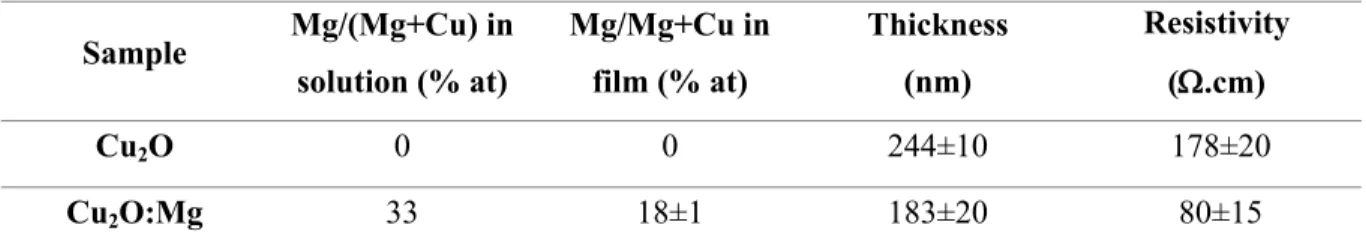
The as-deposited films were routinely characterized in order to quantify the Mg content, thickness and resistivity of the films (Table 1). Both Cu2O and Cu2O:Mg as-deposited films
presented a yellow colour under ambient light (see Figure S1 in Supporting Information).
3 4 5 6 7 8 9 10 11 12 13 14 15 16 17 18 19 20 21 22 23 24 25 26 27 28 29 30 31 32 33 34 35 36 37 38 39 40 41 42 43 44 45 46 47 48 49 50 51 52 53 54 55 56 57 58 59 60
Table 1 General properties of as-deposited Cu2O and Cu2O:Mg films for the stability study Sample Mg/(Mg+Cu) in solution (% at) Mg/Mg+Cu in film (% at) Thickness (nm) Resistivity (.cm) Cu2O 0 0 244±10 178±20 Cu2O:Mg 33 18±1 183±20 80±15
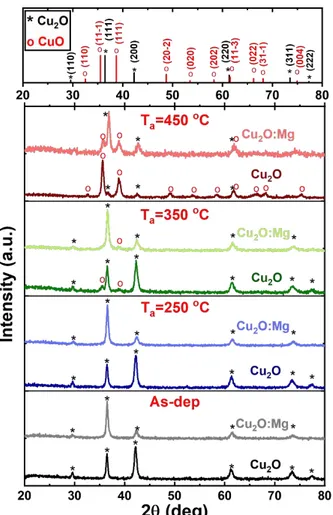
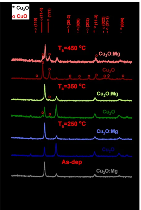
The films were then cut in four different specimen and three different specimens of each film were annealed at 250 ºC, 350 ºC and 450 ºC for 30 minutes in air. The temperature evolution of the Cu2O and Cu2O:Mg diffraction patterns obtained by GI-XRD is presented in
Figure 1. Only the diffraction peaks corresponding to the Cu2O phase are detected in the
as-deposited film and in the film annealed at 250ºC for both undoped and Mg-doped films. When the annealing temperature increases to 350ºC, two additional diffraction peaks are clearly detected at 35.5 ° and 38.7° for the undoped thin film. They can be attributed to the (11-1) and (111) reflections of the CuO monoclinic phase, respectively. At the same temperature, only a small diffraction peak at 38.7° attributed to the (111) CuO phase is detected in the Mg-doped film. After annealing at 450ºC, the undoped film pattern is mainly composed of ten diffraction peaks associated to the CuO phase and weak residual peaks of Cu2O at 36.4°, 42.3° and 61.3°
corresponding to the (111), (200) and (220) reflections. As for the Cu2O:Mg film, only three
CuO diffraction peaks are detected although the (111) Cu2O reflection remains the most intense
one. It is worth noting that this reflection has been shifted from its original and theoretical position at 36.42º to 36.84º. This result gives evidence of a modification of the lattice parameter from 4.270 Å to 4.226 Å. No significant shift of the (111) Cu2O reflection was observed for
other samples annealed at lower temperatures.
3 4 5 6 7 8 9 10 11 12 13 14 15 16 17 18 19 20 21 22 23 24 25 26 27 28 29 30 31 32 33 34 35 36 37 38 39 40 41 42 43 44 45 46 47 48 49 50 51 52 53 54 55 56 57 58 59
Figure 1 GI-XRD patterns of undoped and Mg-doped Cu2O thin films deposited on glass corresponding
to the as-deposited and annealed samples (250, 350 and 450°C). The reference patterns of Cu2O (cubic, space
group Pn-3m, JCPDS n° 04-007-9767) and CuO (monoclinic, space group C2/c, ICDD n° 00-048-1548) are shown at the top. Cu2O and CuO reflections are marked with * and o, respectively.
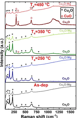
Raman spectroscopy was used to clarify the early stage of the phase transformation in these sets of samples. This technique is complementary to XRD analysis as it allows a local analysis. Raman spectra of as-deposited and annealed Cu2O and Cu2O:Mg thin films are shown
in Figure 2. In agreement with XRD results and independently of the doping, Raman spectra of as-deposited and 250°C annealed films are only composed of lines characteristic of the Cu2O
phase, at 109, 149, 190, 217, 298, 417, 496, 646 and 798 cm-1.27 A decrease of the lines intensity
is observed for the doped film in comparison with the undoped one. After annealing at 350°C, the Raman spectrum of the Cu2O:Mg film appears unchanged whereas one additional line is
barely detected at 348 cm-1 for the undoped film. It can be assigned to the B
g1 mode of CuO.
The CuO Raman spectrum is composed of three modes at 296 cm-1 (A
g), 350 cm-1 (Bg1) and 632
cm-1 (B
g2)33,34 and the peak at 350 cm-1 is the only one which can be used to differentiate CuO
from Cu2O, since the two other ones have positions very close to Cu2O modes. After annealing
at 450°C, the spectrum of the undoped film only contains the three CuO modes whereas in the case of Cu2O:Mg, the Bg1 CuO mode occurs in addition to the Cu2O lines, which are still present 3 4 5 6 7 8 9 10 11 12 13 14 15 16 17 18 19 20 21 22 23 24 25 26 27 28 29 30 31 32 33 34 35 36 37 38 39 40 41 42 43 44 45 46 47 48 49 50 51 52 53 54 55 56 57 58 59 60
and form the majority of the detected Raman modes. It must be noted that a wide fluorescence band is systematically observed in spectra of the Mg-doped films whatever the as-deposited or annealed state. It can be related to electronic defects in the films rather than to organic residues coming from the precursors, which would be decomposed at such annealing temperatures.
Figure 2 Raman spectra of the undoped and Mg-doped Cu2O thin films deposited on glass corresponding
to the as-deposited and annealed samples (250, 350 and 450°C). Cu2O and CuO peaks are marked with * and o,
respectively.
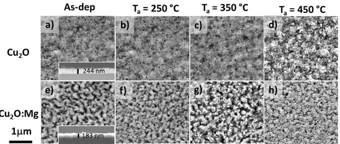
In order to evaluate the doping effect on the film morphology, SEM observations of the undoped and doped as-deposited and annealed films were carried out. The SEM images corresponding to the undoped Cu2O films are shown in Figure 3 a) to d). The cross-section of
the as-deposited film in the inset of Figure 3 a) shows a homogeneous layer with an average thickness of 244±10 nm. This film observed in top-view, Figure 3 a), shows a porous surface with hardly visible grains, which remains unchanged after annealing at 250°C (Figure 3 b)). The increase of the annealing temperature to 350°C led to film changes: small grains are now visible and the porosity seems to be reduced (Figure 3c)). The film annealed at 450°C shows larger grains with an average size in the 100 nm range, forming a rougher structure when
3 4 5 6 7 8 9 10 11 12 13 14 15 16 17 18 19 20 21 22 23 24 25 26 27 28 29 30 31 32 33 34 35 36 37 38 39 40 41 42 43 44 45 46 47 48 49 50 51 52 53 54 55 56 57 58 59
compared to previous samples (Figure 3d)). The observation of the formation and growth of new grains is consistent with the formation of the CuO phase on top of the Cu2O thin films.
SEM micrographs of Mg-doped Cu2O films are presented in Figure 3 e) to h). The
cross-section of the as-deposited film in the inset of Figure 3e) shows a rougher and more irregular layer in comparison with the undoped film, with an average thickness of 183±20nm. This uneven morphology was also confirmed in the top view image, where a rough surface with larger grains is visible (Figure 3 e)) and is retained after annealing at 250°C (Figure 3 f)). This effect of the dopant has been already observed for Sr-doped and Mg-doped Cu2O thin films.27,29
When the thermal treatment is performed at 350°C (Figure 3 g)), small grains with sizes smaller than 100 nm start to appear on the top of the original morphology, covering 26% of the film surface. The image quantification was obtained by using ImageJ software (see Figure S2 in Supporting Information). The film annealed at 450°C shows its surface completely covered with grains of an approximate size below 100nm (Figure 3 h)), smaller than in the undoped Cu2O films. The uniform distribution of the small grains on the film surface maintains a
roughness similar to that obtained for the Cu2O:Mg as-deposited thin film.
Figure 3 SEM micrographs of Cu2O and Cu2O:Mg thin films. Top views of as-deposited film with
cross-section in inset: Cu2O in a) and Cu2O:Mg in e). Annealed films at 250ºC, 350ºC and 450ºC: Cu2O in b), c), and
d) and Cu2O:Mg in f), g) and h), respectively.
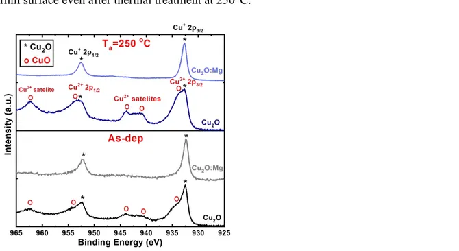
XPS was used to detect the chemical changes and determine the Cu oxidation state in the upper 10 nm of the films. As-deposited and 250 ºC annealed samples were selected for this analysis in order to give an insight into the beginning of the transformation of Cu2O into CuO.
The Cu oxidation state was analysed by scanning the Cu 2p spectra without etching the film surface. Spectra of the as-deposited and 250°C annealed films are presented in Figure 4. In the case of undoped films, the Cu doublet assigned to the Cu 2p3/2 and Cu 2p1/2 states is 3 4 5 6 7 8 9 10 11 12 13 14 15 16 17 18 19 20 21 22 23 24 25 26 27 28 29 30 31 32 33 34 35 36 37 38 39 40 41 42 43 44 45 46 47 48 49 50 51 52 53 54 55 56 57 58 59 60
accompanied by satellites at 940-945 eV, clearly indicating the presence of Cu2+ at the film
surface,35 even in the as-deposited thin films. The Cu 2p doublet is composed by two
contributions corresponding to Cu+ and Cu2+. After thermal treatment at 250°C, the intensity of
all the Cu2+ peaks increases, indicating an increase of CuO at the film surface. The spectra
obtained at the surface of the Cu2O:Mg films before and after annealing are similar and contain
only the doublet peaks characteristic of Cu+, i.e. two narrow peaks at 932 eV and at 952 eV
without any satellite.35 This result confirms that the CuO phase is not present at the Cu
2O:Mg
film surface even after thermal treatment at 250°C.
Figure 4 Cu 2p XPS spectra obtained for the undoped and Mg-doped Cu2O thin films deposited on glass,
both as-deposited and annealed at 250°C.
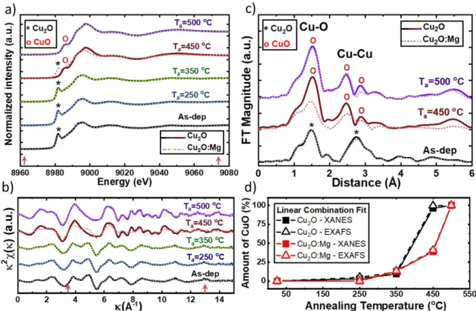
X-ray absorption spectroscopy (XAS) has been used to complete XPS results as it probes the full thickness of the films and provide an element-selective information on the atomic local environment of the atoms. XAS spectra of undoped and Mg-doped Cu2O films,
as-deposited and annealed at several temperatures, were analysed at the Cu-K edge (8978.9 eV). Two extra samples of Cu2O and Cu2O:Mg were annealed at 500 °C for 30 minutes. This
temperature allows to obtain the complete oxidation of the layers and thus, CuO reference films for both sets of samples.
The X-ray Absorption Near Edge Structure (XANES) spectra of the films are presented in Figure 5 a). The edge energy position (E0) is taken as the first maximum in the first derivative
spectrum (see Figure S3 in Supporting Information). A shift of E0 from 8980.8 eV to 8984.1
eV is observed with increasing annealing temperature for both groups of samples. This E0 shift
arises from the modification of the Cu linear coordination in Cu2O, similar to that reported from 3 4 5 6 7 8 9 10 11 12 13 14 15 16 17 18 19 20 21 22 23 24 25 26 27 28 29 30 31 32 33 34 35 36 37 38 39 40 41 42 43 44 45 46 47 48 49 50 51 52 53 54 55 56 57 58 59
other studies in the Cu-O system.36,37 The change in the oxidation state of the copper atom, from
Cu+ into Cu2+, leads to the observed 3.3eV shift of the edge energy position, as confirmed by
experimental38 and theoretical studies.39
The Extended X-ray absorption Fine Structure (EXAFS) spectra – extracted via the standard background removal procedure - are shown in Figure 5 b). The XANES and EXAFS spectra versus the annealing temperature are identical for both Cu2O and Cu2O:Mg thin films,
except the 450 °C annealing step. In particular, a little deviation from Cu2O is observed in
comparison with the as-deposited up to 350 °C annealed spectra while a full conversion to CuO occurs at 500 °C for both types of films. The 450 °C annealing step is different for Cu2O and
Cu2O:Mg thin films. At 450 °C, Cu2O thin films show a full conversion to CuO, while the
Mg-doped thin films show a mixed character. This is visible in Figure 5 c), where the amplitude of the Fourier Transform of the EXAFS data (FT) in the range 3.5 to 13 Å-1 is shown for the 450
°C annealing step, compared to the as-deposited and the 500 °C one. The FT may be associated to an average radial distribution function around the absorbing atoms (Cu), with the caveat that the distance scale is not correct, due to the absence of the phase correction. The first peak in the FT, corresponding to a neighbour distance between 1 and 2 Å, is identified as the oxygen first neighbour (Cu-O 1st) for Cu
2O and CuO. There is an increase of the peak intensity combined
with a small shift to higher distances, related to the structural changes associated with the phase transformation: a higher number of O neighbouring atoms between the Cu2O and CuO,
changing from 2 to 4, as well as an increase of the Cu-O distance, from 1.85Å in Cu2O to 1.95Å
in CuO. The second peak, corresponding to a neighbour distance between 2 and 4 Å, is attributed to copper neighbour atoms (Cu-Cu 1st). When Cu
2O transforms into CuO, the peak
splits into two parts, attributed to copper neighbours of higher order (1st, 2nd and 3rd), as well as
3rd order O neighbours. In the case of Mg-doped Cu
2O film annealed at 450 °C, there is an
intermediate state for both peaks, Cu-O 1st and Cu-Cu 1st, represented in Figure 5 c), which
were undetected in any spectrum of the undoped Cu2O samples. Nevertheless, this is an
over-simplified qualitative evaluation in order to give a simple visual interpretation of the evolution of the spectra from as-deposited Cu2O to the 500 °C annealed CuO. By this simple approach is
possible to visually compare the case at 450 °C, showing differences with the Mg doping: Cu-O group less intense and Cu-Cu group less “split” peaks, which is a signature of the less amount of CuO. The peaks shown in the Fourier Transform amplitude, Figure 5 c), are generated by the sum of the photoelectron scattering paths (single and multiple) from the absorbing Cu atoms, corresponding to an average ensemble of distances.
3 4 5 6 7 8 9 10 11 12 13 14 15 16 17 18 19 20 21 22 23 24 25 26 27 28 29 30 31 32 33 34 35 36 37 38 39 40 41 42 43 44 45 46 47 48 49 50 51 52 53 54 55 56 57 58 59 60
Figure 5 Cu K-edge XAS data and linear combination fits for the undoped (solid lines) and Mg-doped Cu2O (dotted lines) thin films corresponding to the as-deposited and annealed samples (250, 350, 450 and 500
°C). a) XANES region, b) k2weighted EXAFS spectra and c) amplitude – not phase corrected – of the Fourier
transform (selected subset of data) in the k-range 3.5-13 Å-1. Red arrows represent the energy range and k-range
employed for the linear combination fits. d) Results of the linear combination fits of the Cu2O and CuO
experimental reference spectra (cf. main text).
To quantify the amount of CuO formed in the films during the thermal annealing, a linear combination fit (LCF) for both XANES and EXAFS spectra was performed, using as basis set the Cu2O and CuO reference spectra. For the Cu2O case, the undoped Cu2O
as-deposited spectrum was employed as reference; while we selected the spectrum of undoped Cu2O annealed at 500 °C for CuO reference, due to its complete transformation into CuO. The
k2 and Fourier Transform of the Cu
2O and CuO reference spectra show a good agreement with
the respective Cu2O and CuO simulated spectra from each crystal structure (see Figure S4 in
the Supporting Information). The fit range was -30 to +80 eV with respect to E0 for the
normalized XANES, and 3.5 to 13 Å-1 for the k2weighted EXAFS, i.e. k2k The fits were
performed using the Athena software 40. The LCF method takes into account, for each Cu 2O
and CuO phase, the full multiple scattering configuration; for this reason and in this particular case, this method is superior to a simplified scattering path expansion fit. The results obtained from the XANES and EXAFS LCF are shown in Figure 5 d), and the single plots of the fits with the corresponding residuals are plotted in the Supplementary Information (Figures S5 and
3 4 5 6 7 8 9 10 11 12 13 14 15 16 17 18 19 20 21 22 23 24 25 26 27 28 29 30 31 32 33 34 35 36 37 38 39 40 41 42 43 44 45 46 47 48 49 50 51 52 53 54 55 56 57 58 59
S6). The combined error bars are below 1% (smaller than the symbol size in Figure 5d). For annealing temperature up to 350 °C, both films present similar quantities of CuO, linearly increasing up to 12(1)%. We can observe a substantial difference in the CuO amount between the two films annealed at 450 °C, where the undoped sample presents almost full conversion from Cu2O to the CuO phase, that is, 98(1)%. In the Mg-doped Cu2O film, we observe a
drastically lower amount of CuO, that is, 40(1)%. This result agrees with the position of the edge energy in the XANES spectra.
4. Discussion
A detailed analysis of the results obtained in this study allowed us to provide a comprehensive model for the magnesium incorporation and the related effects on the stability of the Cu2O phase under different annealing treatments.
The direct comparison of the annealing effects on both sets of samples gives evidence of some differences in terms of growth of the CuO phase. The morphological analysis obtained by SEM images combined with the structural results provided by XRD, Raman, XANES and EXAFS suggests that the formation of CuO is associated to the formation of smaller and brighter grains at the film surface. The formation of these grains takes place differently in the two samples annealed at 350 ºC. In the undoped film, the new grains seem to grow on the whole surface of the film while in the Mg-doped films, the CuO grains are only formed in places representing around 26% of the visible surface. For the Cu2O:Mg films, an annealing
temperature of 450 ºC is needed to obtain a morphology similar to that of the undoped sample annealed at 350 ºC, consisting in small grains covering completely the film surface. Moreover, the undoped Cu2O films annealed at 450ºC show a different aspect and exhibit larger CuO
grains, which is consistent with a higher degree of phase transformation as shown in the GI-XRD and Raman results. We can generalize the formation of CuO for temperatures below 350°C in both undoped and Mg-doped thin films, but with different kinetics.
The different behaviours in both sets of samples led us to identify two distinct mechanisms for the CuO formation. On the one hand, the undoped thin films transform into CuO by oxidation both at the film surface and in the bulk. At the film surface, the Cu+ cations
are easily oxidized into Cu2+ in contact with oxygen forming the CuO phase. This was
confirmed by the XPS analysis, which reveals the presence of Cu2+ even in the as-deposited
samples. The presence of magnesium seems to affect the surface of the Cu2O thin film even
before any thermal annealing, as the Cu2+ signature in XPS spectrum is absent for the Cu
2O:Mg 3 4 5 6 7 8 9 10 11 12 13 14 15 16 17 18 19 20 21 22 23 24 25 26 27 28 29 30 31 32 33 34 35 36 37 38 39 40 41 42 43 44 45 46 47 48 49 50 51 52 53 54 55 56 57 58 59 60
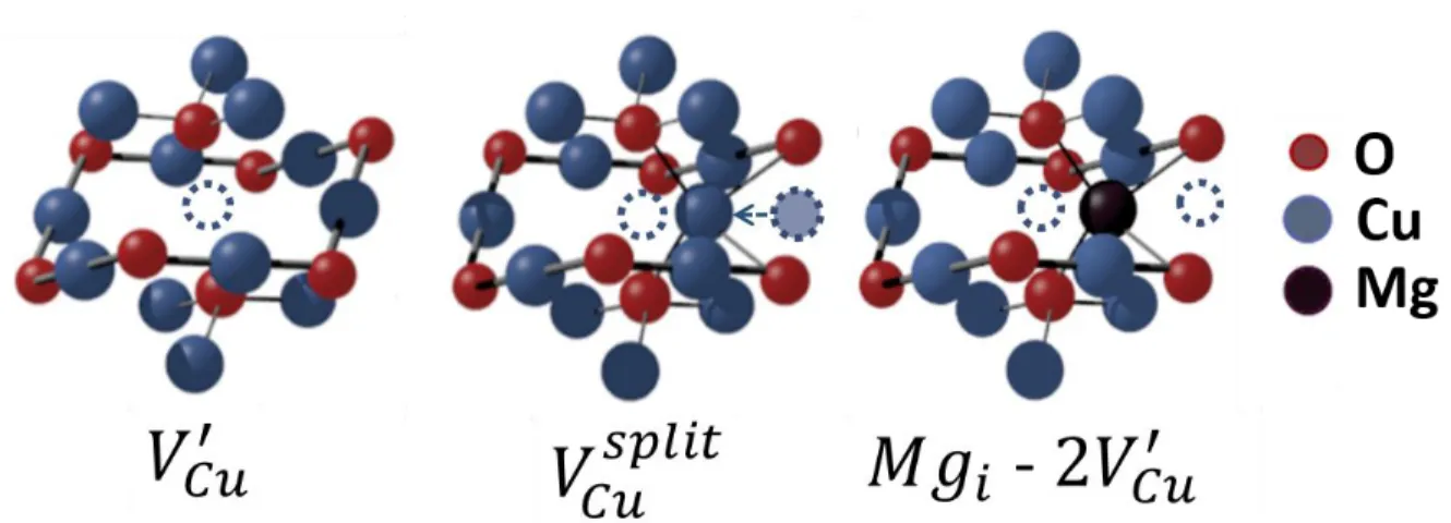
as-deposited thin film. Apart from the surface, the formation of split copper vacancies is required to induce the formation of Cu2+ centres and then create CuO nucleation centres inside
the grains. The split copper vacancies, represented in Figure 6, lead to an inefficient generation of free holes due to the highly localized character of this type of defect,5,6 which later contributes
to the formation of the parasitic CuO phase throughout the film. In the presence of Mg, the transformation seems to start only at the film surface, at 350°C, while simple copper vacancies (Figure 6) are the major defects created inside the film thanks to the presence of the dopant.
As suggested by Isseroff and Carter, Mg doping can prevent the formation of split vacancies for a single cation vacancy, since the divalent cation would be placed in a site similar to a split copper vacancy in the crystal structure.6 This fact seems to be confirmed by the
resilience of Cu2O to preserve its cubic structure. The inhibition to create split vacancies would
thus reduce the CuO parasitic centres inside the film, this being the main mechanism for the phase transformation during the annealing stages. Additionally, in the Cu2O:Mg thin film
annealed at 450 °C, a change in lattice parameters was observed by XRD. This suggests structural modifications in the Cu2O crystal structure resulting in the formation of a new type
of defect in the film. One possible defect is a clustering of a second simple copper vacancy with the Mg atom in a tetrahedral position, [Mgi − 2·VCu]−,which has been proposed by Isseroff and
Carter.6 Still, the nature of copper vacancies level is yet to be fully understood. A representation
of both Cu2O defects is shown in Figure 6, as well as the suggested [Mgi − 2·VCu]− complex.
Figure 6 Representation of a single copper vacancy (𝑉′𝐶𝑢), a split copper vacancy (𝑉𝑠𝑝𝑙𝑖𝑡) and a 𝐶𝑢
magnesium incorporation in a tetrahedral site [Mgi − 2·VCu]−. Copper atoms are represented by blue circles,
oxygen as red ones and magnesium as black ones.
5. Conclusion
Post-deposition annealing treatments in oxidizing conditions are commonly performed on Cu2O thin films to enhance electrical and optical properties; nevertheless, a parasitic CuO 3 4 5 6 7 8 9 10 11 12 13 14 15 16 17 18 19 20 21 22 23 24 25 26 27 28 29 30 31 32 33 34 35 36 37 38 39 40 41 42 43 44 45 46 47 48 49 50 51 52 53 54 55 56 57 58 59
phase usually starts to be formed in the films at 300 ºC. The presence of the Mg dopant in the films has a substantial impact on the stability of the Cu2O phase under these oxidizing
conditions, as revealed by this study. The formation of the CuO phase is indeed delayed in the Cu2O:Mg thin films when submitted to similar annealing conditions in comparison with the
undoped films. This is due to distinct formation rates of the CuO phase in the undoped and doped films. As suggested by Isseroff and Carter, divalent cation doping such as Mg2+, can
prevent the formation of split copper vacancies, since the cation would be placed in a position similar to a split copper vacancy in the crystal structure. As a consequence, the reduction of split copper vacancies leads to a lower concentration of CuO nucleation centres, which inhibit the formation of the parasitic phase in the bulk of the film.
6. Supporting Information.
Optical appearance of undoped and Mg-doped Cu2O thin films (Figure S1). SEM
micrographs of Mg-doped Cu2O thin films on glass annealed at 350°C (Figure S2).
Determination of E0 in all spectra of undoped and Mg-doped Cu2O thin films on glass (Figure
S3). Fitting of EXAFS reference spectra: Cu2O for as-deposited intrinsic thin film and CuO
obtained by oxidation of Cu2O at 500°C during 30 minutes (Figure S4). List of EXAFS
parameters obtained from fitting of reference spectra: Cu2O for as-deposited intrinsic thin film
and CuO obtained by oxidation of Cu2O at 500°C during 30 minutes (Table S1). Linear
combination fits and correspondent residuals XAS spectra of Cu2O and Cu2O:Mg thin films
(Figure S5 and S6)
7. Acknowledgements
Financial support by the IDS-FunMat scholarship selected under the program “ERASMUS MUNDUS II 2009-2013” is gratefully acknowledged. N. D. N. acknowledges the financial support by the F.R.S-FNRS of Belgium (project J.0124.19) and by the European Joint Doctorate FUNMAT (H2020-MSCA-ITN-2014, Project ID 641640). This project was financially supported by ‘‘Carnot Energies du Futur’’ (SOLAROX project). This work benefited from the facilities and expertise of the OPE)N(RA characterization platform of FMNT (FR 2542, fmnt.fr) supported by CNRS, Grenoble INP and UGA. We thank Synchrotron ESRF for general facilities. The experiment at the FAME (BM30B) beamline, proposal number 30-02-1122, benefited from the French beamtime allocation via the SOLEIL committee. The authors would like to warmly thank Hervé Roussel for the grazing incidence X-ray diffraction measurements. 3 4 5 6 7 8 9 10 11 12 13 14 15 16 17 18 19 20 21 22 23 24 25 26 27 28 29 30 31 32 33 34 35 36 37 38 39 40 41 42 43 44 45 46 47 48 49 50 51 52 53 54 55 56 57 58 59 60
8. References
(1) Minami, T.; Nishi, Y.; Miyata, T. Cu2O-Based Solar Cells Using Oxide Semiconductors. J. Semicond. 2016, 37 (1). https://doi.org/10.1088/1674-4926/37/1/014002.
(2) Nandy, S.; Banerjee, A.; Fortunato, E.; Martins, R. A Review on Cu2O and Cu-Based
p-Type Semiconducting Transparent Oxide Materials: Promising Candidates for New Generation Oxide Based Electronics. Rev. Adv. Sci. Eng. 2013, 2 (4), 273–304. https://doi.org/10.1166/rase.2013.1045.
(3) Biccari, F.; Malerba, C.; Mittiga, A. Defects and Doping in Cu2O: General Properties
and Applications. 2009, No. 688774, 1–28. https://doi.org/10.1016/0038-1098(70)90325-X.
(4) Scanlon, D. O.; Walsh, A.; Watson, G. W. Understanding the P-Type Conduction Properties of the Transparent Conducting Oxide CuBO2: A Density Functional
Theoryanalysis. Chem. Mater. 2009, 21 (19), 4568–4576.
https://doi.org/10.1021/cm9015113.
(5) Scanlon, D. O.; Morgan, B. J.; Watson, G. W.; Walsh, A. Acceptor Levels in P-Type Cu2O: Rationalizing Theory and Experiment. Phys. Rev. Lett. 2009, 103 (9), 1–4.
https://doi.org/10.1103/PhysRevLett.103.096405.
(6) Isseroff, L. Y.; Carter, E. A. Electronic Structure of Pure and Doped Cuprous Oxide with Copper Vacancies: Suppression of Trap States. Chem. Mater. 2013, 25 (3), 253–265. https://doi.org/10.1021/cm3040278.
(7) Nolan, M.; Elliott, S. D. The P-Type Conduction Mechanism in Cu2O: A First Principles
Study. Phys. Chem. Chem. Phys. 2006, 8 (45), 5350–5358.
https://doi.org/10.1039/b611969g.
(8) Figueiredo, V.; Elangovan, E.; Gonçalves, G.; Barquinha, P.; Pereira, L.; Franco, N.; Alves, E.; Martins, R.; Fortunato, E. Effect of Post-Annealing on the Properties of Copper Oxide Thin Films Obtained from the Oxidation of Evaporated Metallic Copper.
Appl. Surf. Sci. 2008, 254 (13), 3949–3954.
https://doi.org/10.1016/j.apsusc.2007.12.019.
(9) Wang, Y.; Miska, P.; Pilloud, D.; Horwat, D.; Mücklich, F.; Pierson, J. F. Transmittance Enhancement and Optical Band Gap Widening of Cu O Thin Films after Air Annealing.
3 4 5 6 7 8 9 10 11 12 13 14 15 16 17 18 19 20 21 22 23 24 25 26 27 28 29 30 31 32 33 34 35 36 37 38 39 40 41 42 43 44 45 46 47 48 49 50 51 52 53 54 55 56 57 58 59
J. Appl. Phys. 2014, 115 (7), 2–7. https://doi.org/10.1063/1.4865957.
(10) Johan, M. R.; Suan, M. S. M.; Hawari, N. L.; Ching, H. A. Annealing Effects on the Properties of Copper Oxide Thin Films Prepared by Chemical Deposition. Int. J. Electrochem. Sci. 2011, 6 (12), 6094–6104. https://doi.org/10.1088/0268-1242/20/5/012.
(11) Eisermann, S.; Kronenberger, A.; Laufer, A.; Bieber, J.; Haas, G.; Lautenschläger, S.; Homm, G.; Klar, P. J.; Meyer, B. K. Copper Oxide Thin Films by Chemical Vapor Deposition: Synthesis, Characterization and Electrical Properties. Phys. Status Solidi
2012, 209 (3), 531–536. https://doi.org/10.1002/pssa.201127493.
(12) Wang, J.; Li, C.; Zhu, Y.; Boscoboinik, J. A.; Zhou, G. Insight into the Phase Transformation Pathways of Copper Oxidation: From Oxygen Chemisorption on the Clean Surface to Multilayer Bulk Oxide Growth. J. Phys. Chem. C 2018, 122, 26519– 26527. https://doi.org/10.1021/acs.jpcc.8b09145.
(13) Meyer, B. K.; Polity, A.; Reppin, D.; Becker, M.; Hering, P.; Klar, P. J.; Sander, T.; Reindl, C.; Benz, J.; Eickhoff, M.; et al. Binary Copper Oxide Semiconductors: From Materials towards Devices. Phys. Status Solidi 2012, 249 (8), 1487–1509. https://doi.org/10.1002/pssb.201248128.
(14) Camacho-Espinosa, E.; Rimmaudo, I.; Riech, I.; Mis-Fernández, R.; Peña, J. L. Stability of Sputter Deposited Cuprous Oxide (Cu2O) Subjected to Ageing Conditions for
Photovoltaic Applications. J. Appl. Phys. 2018, 123 (8).
https://doi.org/10.1063/1.5017538.
(15) Deuermeier, J.; Wardenga, H. F.; Morasch, J.; Siol, S.; Nandy, S.; Calmeiro, T.; Martins, R.; Klein, A.; Fortunato, E. Highly Conductive Grain Boundaries in Copper Oxide Thin Films. J. Appl. Phys. 2016, 119 (23). https://doi.org/10.1063/1.4954002.
(16) Deuermeier, J.; Liu, H.; Rapenne, L.; Calmeiro, T.; Renou, G.; Martins, R.; Muñoz-Rojas, D.; Fortunato, E. Visualization of Nanocrystalline CuO in the Grain Boundaries of Cu 2 O Thin Films and Effect on Band Bending and Film Resistivity. APL Mater.
2018, 6 (9), 096103. https://doi.org/10.1063/1.5042046.
(17) Rehman, S.; Hur, J. H.; Kim, D. K. Resistive Switching in Solution-Processed Copper Oxide (CuxO) by Stoichiometry Tuning. J. Phys. Chem. C 2018, 122 (20), 11076–11085.
https://doi.org/10.1021/acs.jpcc.8b00432. 3 4 5 6 7 8 9 10 11 12 13 14 15 16 17 18 19 20 21 22 23 24 25 26 27 28 29 30 31 32 33 34 35 36 37 38 39 40 41 42 43 44 45 46 47 48 49 50 51 52 53 54 55 56 57 58 59 60
(18) Chatterjee, S.; Saha, S. K.; Pal, A. J. Formation of All-Oxide Solar Cells in Atmospheric Condition Based on Cu2O Thin-Films Grown through SILAR Technique. Sol. Energy Mater. Sol. Cells 2016, 147, 17–26. https://doi.org/10.1016/j.solmat.2015.11.045. (19) Nishi, Y.; Miyata, T.; Minami, T. The Impact of Heterojunction Formation Temperature
on Obtainable Conversion Efficiency in N-ZnO/p-Cu2O Solar Cells. Thin Solid Films
2013, 528, 72–76. https://doi.org/10.1016/j.tsf.2012.09.090.
(20) Zang, Z. Efficiency Enhancement of ZnO/Cu2O Solar Cells with Well Oriented and
Micrometer Grain Sized Cu2O Films. Appl. Phys. Lett. 2018, 112 (4), 42106.
(21) Yu, L.; Xiong, L.; Yu, Y. Cu2O Homojunction Solar Cells: F-Doped N-Type Thin Film
and Highly Improved Efficiency. J. Phys. Chem. C 2015, 119 (40), 22803–22811. https://doi.org/10.1021/acs.jpcc.5b06736.
(22) Minami, T.; Miyata, T.; Nishi, Y. Relationship between the Electrical Properties of the N-Oxide and p-Cu2O Layers and the Photovoltaic Properties of Cu2O-Based
Heterojunction Solar Cells. Sol. Energy Mater. Sol. Cells 2016, 147, 85–93. https://doi.org/10.1016/j.solmat.2015.11.033.
(23) Tadatsugu, M.; Yuki, N.; Toshihiro, M. Efficiency Enhancement Using a Zn1-xGexO
Thin Film as an n-Type Window Layer in Cu2O-Based Heterojunction Solar Cells. Appl. Phys. Express 2016, 9 (5), 52301.
(24) Minami, T.; Nishi, Y.; Miyata, T. High-Efficiency Cu2O-Based Heterojunction Solar
Cells Fabricated Using a Ga2O3 Thin Film as N-Type Layer. Appl. Phys. Express 2013, 6 (4), 044101. https://doi.org/10.7567/APEX.6.044101.
(25) Malerba, C.; Azanza Ricardo, C. L.; Dincau, M.; Biccari, F.; Scardi, P.; Mittiga, A. Nitrogen Doped Cu2O: A Possible Material for Intermediate Band Solar Cells? Sol. Energy Mater. Sol. Cells 2012, 105, 192–195. https://doi.org/10.1016/j.solmat.2012.06.017.
(26) Zang, Z.; Nakamura, A.; Temmyo, J. Single Cuprous Oxide Films Synthesized by Radical Oxidation at Low Temperature for PV Application. 2013, 21 (9), 3352–3358. https://doi.org/10.1364/OE.21.011448.
(27) Bergerot, L.; Jiménez, C.; Chaix-Pluchery, O.; Rapenne, L.; Deschanvres, J.-L. Growth and Characterization of Sr-Doped Cu2O Thin Films Deposited by Metalorganic
Chemical Vapor Deposition. Phys. Status Solidi 2015, 212 (8), 1735–1741.
3 4 5 6 7 8 9 10 11 12 13 14 15 16 17 18 19 20 21 22 23 24 25 26 27 28 29 30 31 32 33 34 35 36 37 38 39 40 41 42 43 44 45 46 47 48 49 50 51 52 53 54 55 56 57 58 59
https://doi.org/10.1002/pssa.201431750.
(28) Brochen, S.; Bergerot, L.; Favre, W.; Resende, J.; Jiménez, C.; Deschanvres, J.-L.; Consonni, V. Effect of Strontium Incorporation on the P-Type Conductivity of Cu2O
Thin Films Deposited by Metal–Organic Chemical Vapor Deposition. J. Phys. Chem. C
2016, 120 (31), 17261–17267. https://doi.org/10.1021/acs.jpcc.6b05479.
(29) Resende, J.; Jiménez, C.; Nguyen, N. D.; Deschanvres, J.-L. Magnesium-Doped Cuprous Oxide (Mg:Cu2O) Thin Films as a Transparent p-Type Semiconductor. Phys. Status Solidi 2016, 7, 1–7. https://doi.org/10.1002/pssa.201532870.
(30) Nolan, M.; Elliott, S. D. Tuning the Transparency of Cu2O with Substitutional Cation
Doping. Chem. Mater. 2008, 20 (17), 5522–5531. https://doi.org/10.1021/cm703395k. (31) Kardarian, K.; Nunes, D.; Maria Sberna, P.; Ginsburg, A.; Keller, D. A.; Vaz Pinto, J.;
Deuermeier, J.; Anderson, A. Y.; Zaban, A.; Martins, R.; et al. Effect of Mg Doping on Cu2O Thin Films and Their Behavior on the TiO2/Cu2O Heterojunction Solar Cells. Sol.
Energy Mater. Sol. Cells 2016, 147, 27–36.
https://doi.org/10.1016/j.solmat.2015.11.041.
(32) Xpsfitting.com. Cu(0): Cu(II) or Cu(I):Cu(II) Calculations
http://www.xpsfitting.com/2012/01/cu0cuii-or-cuicuii-calculations.html (accessed Aug 21, 2017).
(33) Goldstein, H. F.; Dai-sik, K.; Peter, Y. Y.; Bournet, L. C. Raman Study of CuO Single Crystals. Phys. Rev. B 1990, 41 (10).
(34) Guha, S.; Peebles, D.; Wieting, T. J. Zone-Center (Q=0) Optical Phonons in CuO Studied by Raman and Infrared Spectroscopy. Phys. Rev. B 1991, 43 (16), 13092–13101. https://doi.org/10.1103/PhysRevB.43.13092.
(35) Morales, J.; Barranco, A.; Caballero, A.; Holgado, J. P.; Gonza, a R. Interface Effects for Cu , CuO , and Cu2O Deposited on SiO2 and ZrO2 . XPS Determination of the
Valence State of Copper in Cu / SiO2 and Cu / ZrO2 Catalysts. J. Phys. Chem. B 2002, 106, 6921–6929. https://doi.org/10.1021/jp014618m.
(36) Kim, J. Y.; Rodriguez, A.; Hanson, J. C.; Frenkel, A. I.; Lee, P. L. Reduction of CuO and Cu2O with H2: H Embedding and Kinetic Effects in the Formation of Suboxides.
2003, 10684–10692. 3 4 5 6 7 8 9 10 11 12 13 14 15 16 17 18 19 20 21 22 23 24 25 26 27 28 29 30 31 32 33 34 35 36 37 38 39 40 41 42 43 44 45 46 47 48 49 50 51 52 53 54 55 56 57 58 59 60
(37) Tolentino, H.; Medarde, M.; Fontaine, A.; Baudelet, F.; Dartyge, E.; Guay, D.; Tourillon, G. Anisotropy of the Core-Hole Relaxation in x-Ray-Absorption Spectroscopy as Probed in Square Planar Cuprates. Phys. Rev. B 1992, 45 (14), 8091–8096. https://doi.org/10.1103/PhysRevB.45.8091.
(38) Akeyama, K.; Kuroda, H.; Kosugi, N. Cu K-Edge XANES and Electronic Structure of Trivalent, Divalent, and Monovalent Cu Oxides. Jpn. J. Appl. Phys. 1993, 32 (S2), 98. https://doi.org/10.7567/jjaps.32s2.98.
(39) Rudolph, J.; Jacob, C. R. Revisiting the Dependence of Cu K ‑ Edge X ‑ Ray Absorption Spectra on Oxidation State and Coordination Environment. Inorg. Chem. 2018, 57, 10591–10607. https://doi.org/10.1021/acs.inorgchem.8b01219.
(40) Ravel, B.; Newville, M. ATHENA, ARTEMIS, HEPHAESTUS: Data Analysis for X-Ray Absorption Spectroscopy Using IFEFFIT. J. Synchrotron Radiat. 2005, 12 (4), 537– 541.
TOC Graphic
3 4 5 6 7 8 9 10 11 12 13 14 15 16 17 18 19 20 21 22 23 24 25 26 27 28 29 30 31 32 33 34 35 36 37 38 39 40 41 42 43 44 45 46 47 48 49 50 51 52 53 54 55 56 57 58 59TOC 599x331mm (49 x 49 DPI) 3 4 5 6 7 8 9 10 11 12 13 14 15 16 17 18 19 20 21 22 23 24 25 26 27 28 29 30 31 32 33 34 35 36 37 38 39 40 41 42 43 44 45 46 47 48 49 50 51 52 53 54 55 56
Figure 1 GI-XRD patterns of undoped and Mg-doped Cu2O thin films deposited on glass corresponding to the as-deposited and annealed samples (250, 350 and 450°C). The reference patterns of Cu2O (cubic, space group Pn-3m, JCPDS n° 04-007-9767) and CuO (monoclinic, space group C2/c, ICDD n° 00-048-1548) are
shown at the top. Cu2O and CuO reflections are marked with * and o, respectively. 300x449mm (150 x 150 DPI) 3 4 5 6 7 8 9 10 11 12 13 14 15 16 17 18 19 20 21 22 23 24 25 26 27 28 29 30 31 32 33 34 35 36 37 38 39 40 41 42 43 44 45 46 47 48 49 50 51 52 53 54 55
Figure 2 Raman spectra of the undoped and Mg-doped Cu2O thin films deposited on glass corresponding to the as-deposited and annealed samples (250, 350 and 450°C). Cu2O and CuO peaks are marked with * and
o, respectively. 399x599mm (150 x 150 DPI) 3 4 5 6 7 8 9 10 11 12 13 14 15 16 17 18 19 20 21 22 23 24 25 26 27 28 29 30 31 32 33 34 35 36 37 38 39 40 41 42 43 44 45 46 47 48 49 50 51 52 53 54 55 56
Figure 3 SEM micrographs of Cu2O and Cu2O:Mg thin films. Top views of as-deposited film with cross-section in inset: Cu2O in a) and Cu2O:Mg in e). Annealed films at 250ºC, 350ºC and 450ºC: Cu2O in b), c),
and d) and Cu2O:Mg in f), g) and h), respectively. 204x87mm (150 x 150 DPI) 3 4 5 6 7 8 9 10 11 12 13 14 15 16 17 18 19 20 21 22 23 24 25 26 27 28 29 30 31 32 33 34 35 36 37 38 39 40 41 42 43 44 45 46 47 48 49 50 51 52 53 54 55
Figure 4 Cu 2p XPS spectra obtained for the undoped and Mg-doped Cu2O thin films deposited on glass, both as-deposited and annealed at 250°C.
296x296mm (150 x 150 DPI) 3 4 5 6 7 8 9 10 11 12 13 14 15 16 17 18 19 20 21 22 23 24 25 26 27 28 29 30 31 32 33 34 35 36 37 38 39 40 41 42 43 44 45 46 47 48 49 50 51 52 53 54 55 56
Figure 5 Cu K-edge XAS data and linear combination fits for the undoped (solid lines) and Mg-doped Cu2O (dotted lines) thin films corresponding to the as-deposited and annealed samples (250, 350, 450 and 500 °C). a) XANES region, b) k2X weighted EXAFS spectra and c) amplitude – not phase corrected – of the Fourier transform (selected subset of data) in the k-range 3.5-13 Å-1. Red arrows represent the energy range and k-range employed for the linear combination fits. d) Results of the linear combination fits of the
Cu2O and CuO experimental reference spectra (cf. main text). 399x263mm (78 x 78 DPI) 3 4 5 6 7 8 9 10 11 12 13 14 15 16 17 18 19 20 21 22 23 24 25 26 27 28 29 30 31 32 33 34 35 36 37 38 39 40 41 42 43 44 45 46 47 48 49 50 51 52 53 54 55
Figure 6 Representation of a single copper vacancy, a split copper vacancy and a magnesium incorporation in a tetrahedral site. Copper atoms are represented by blue circles, oxygen as red ones and magnesium as
black ones. 199x72mm (150 x 150 DPI) 3 4 5 6 7 8 9 10 11 12 13 14 15 16 17 18 19 20 21 22 23 24 25 26 27 28 29 30 31 32 33 34 35 36 37 38 39 40 41 42 43 44 45 46 47 48 49 50 51 52 53 54 55 56
Figure S1 Optical appearance of undoped and Mg-doped Cu2O thin films on glass in the as-deposited and annealed states (250, 350 and 450°C).
174x73mm (150 x 150 DPI) 3 4 5 6 7 8 9 10 11 12 13 14 15 16 17 18 19 20 21 22 23 24 25 26 27 28 29 30 31 32 33 34 35 36 37 38 39 40 41 42 43 44 45 46 47 48 49 50 51 52 53 54 55
Figure S2 a-c) SEM micrographs of Mg-doped Cu2O thin films on glass annealed at 350°C d-f) Determination of CuO coverage area by ImageJ.
262x161mm (150 x 150 DPI) 3 4 5 6 7 8 9 10 11 12 13 14 15 16 17 18 19 20 21 22 23 24 25 26 27 28 29 30 31 32 33 34 35 36 37 38 39 40 41 42 43 44 45 46 47 48 49 50 51 52 53 54 55 56
Figure S3 Normalized XANES spectra (left) and first derivative (right) with the determination of E0 in all spectra of undoped and Mg-doped Cu2O thin films on glass in the as-deposited and annealed states (250,
350, 450°C and 500°C ). 242x181mm (150 x 150 DPI) 3 4 5 6 7 8 9 10 11 12 13 14 15 16 17 18 19 20 21 22 23 24 25 26 27 28 29 30 31 32 33 34 35 36 37 38 39 40 41 42 43 44 45 46 47 48 49 50 51 52 53 54 55
Figure S4 Fitting of reference spectra: Cu2O for as-deposited intrinsic thin film and CuO obtained by oxidation of Cu2O at 500°C during 30 minutes. a) k2X with k window used between 1 and 14 Å-1 and b)
Fourier Transform magnitude in r between 0 and 6 Å. 177x157mm (150 x 150 DPI) 3 4 5 6 7 8 9 10 11 12 13 14 15 16 17 18 19 20 21 22 23 24 25 26 27 28 29 30 31 32 33 34 35 36 37 38 39 40 41 42 43 44 45 46 47 48 49 50 51 52 53 54 55 56
Figure S5 XAS spectra of Cu2O and Cu2O:Mg as-deposited used as Cu2O reference and Cu2O and Cu2O:Mg annealed at 500 °C used as CuO reference. Linear combination fit and correspondening residuals of Cu2O
annealed at 250 °C . 182x137mm (150 x 150 DPI) 3 4 5 6 7 8 9 10 11 12 13 14 15 16 17 18 19 20 21 22 23 24 25 26 27 28 29 30 31 32 33 34 35 36 37 38 39 40 41 42 43 44 45 46 47 48 49 50 51 52 53 54 55
Figure S6 Linear combination fit and corresponding residuals of Cu2O and Cu2O:Mg annealed at 350 and 450 °C. 180x131mm (150 x 150 DPI) 3 4 5 6 7 8 9 10 11 12 13 14 15 16 17 18 19 20 21 22 23 24 25 26 27 28 29 30 31 32 33 34 35 36 37 38 39 40 41 42 43 44 45 46 47 48 49 50 51 52 53 54 55 56