HAL Id: hal-02944773
https://hal.archives-ouvertes.fr/hal-02944773
Submitted on 21 Sep 2020
HAL is a multi-disciplinary open access
archive for the deposit and dissemination of
sci-entific research documents, whether they are
pub-lished or not. The documents may come from
teaching and research institutions in France or
abroad, or from public or private research centers.
L’archive ouverte pluridisciplinaire HAL, est
destinée au dépôt et à la diffusion de documents
scientifiques de niveau recherche, publiés ou non,
émanant des établissements d’enseignement et de
recherche français ou étrangers, des laboratoires
publics ou privés.
Autonomous sensor node powered over WiFi
Florian Grante, Ghalid Idir Abib, Muriel Muller, Nel Samama
To cite this version:
Florian Grante, Ghalid Idir Abib, Muriel Muller, Nel Samama. Autonomous sensor node powered over
WiFi: A use case study. WINSYS 2020: 17th International Conference on Wireless Networks and
Mobile Systems, Jul 2020, Lieusaint, France. pp.127-132, �10.5220/0009804101270132�. �hal-02944773�
Autonomous sensor node powered over WiFi: A use case study
Florian Grante, Ghalid Abib, Muriel Muller and Nel Samama
D´epartement Electronique et Physique (EPh) - T´el´ecom SudParis - Institut Polytechnique de Paris 19, rue Marguerite Perey. 91120, Palaiseau - France
{florian.grante, ghalid.abib, muriel.muller, nel.samama}@telecom-sudparis.eu
Keywords: RF electromagnetic energy, energy harvesting, WiFi, autonomous sensor, Schottky diode, RF/DC rectifier, boost, energy budget analysis
Abstract: This paper presents a new approach to the development of a radio frequency energy harvesting system. Starting from a sensor node to define the constraints of our system such as its energy requirement or its supply voltage, we develop a protocol. It allows us to validate whether it is possible to power such a system with an RF/DC converter. First we study a RF/DC converter capable of converting signals in the ISM band at 2.45 GHz whose ambient power has been previously characterized.
1
INTRODUCTION
The Internet of Things (IoT) is gradually revolution-izing our lives in our daily lives as well as in the in-dustrial, medical, connected city projects and elec-tricity distribution with smart grids. But the explo-sion in the number of connected objects also implies the explosion in the production of batteries, the main source of energy used for these objects. Batteries be-ing a depletable source of energy, requirbe-ing regular maintenance, there is a need to find alternative energy sources that we group together under the concept of Energy Harvesting.
Among the different energy sources, the most commonly harvested one is the solar energy with the development of small organic solar panels, which have the advantage of making the panel flexible and do not require rare-earth element in its design. Also, mechanical energy is well suited for products such as connected switches. We can also find research teams working on thermoelectric energy sources based on the Seebeck effect or the source we will focus on in this paper: Radio Frequency (RF) signal. RF sources like WiFi, GSM, TV... emit electromagnetic waves and surround our environment. A lot of them are wasted and could be converted into DC energy to power specific devices.
During the last 10 years, RF energy harvesting state of the art has evolved from a converter system using TV signals (Parks et al., 2013), which was still very present and powerful in the early 2010’s, to more research in the ISM 2.45 GHz band and GSM 900 /
1800 (Ho et al., 2016) with the emergence of WiFi, 3G, 4G... To our knowledge, the different converter developments are made and characterized for theoret-ical purposes, i.e. they do not take into account the final application in which the converter could be use-ful. This is why we wish to follow a new approach in the study of RF/DC (direct current) converters by concretely characterizing the energy requirement of an application and thus discuss the feasibility of such a system.
We base this work on WiFi energy harvesting in the 2.45 GHz ISM (Industrial, Scientific and Medi-cal) band, focusing on the part after the antenna that we will not discuss here because we can rely on work such as (Kurvey and Kunte, ), (Krakauskas et al., ) or (Shaker et al., ) if needed. We will contextualize our need in Sec.2 where we will present the energy requirement of our sensor and the available ambient WiFi energy. Then, we will study the main problem of an RF/DC converter which is the voltage level ob-tained in Sec.3. Finally, a calculation model capable of determining the data transmission frequency from an application based on measurement of the received ambient signal power is defined Sec.4.
2
CONSTRAINTS
Before taking an in-depth look at our RF/DC con-verter on which we will base our work, we need to put some context by defining the different require-ments for the proper functioning of an IoT (Internet
of Things) sensor node and an inventory of our elec-tromagnetic environment around 2.45 GHz ISM band.
2.1
Sensor node
Let us consider here a sensor node as a platform capa-ble of measuring physical quantities and transmitting its data by radio wave. Great progress has been made in recent years on the architectures and power con-sumption of microcontrollers, MEMS sensors and RF transceivers with the emergence of the term ”ultra low power”.
We will base our study which is reported here on a platform developed by ON Semiconductor: RSL10-SOLARSENS-GEVK (Fig.1). This is a platform containing the BME280 environmental sensor from Bosch Sensortec and the RSL10SIP, a system in a package developed by ON Semiconductor consist-ing of an ARM Cortex-M3 microcontroller and a Bluetooth Low Energy transceiver. A white paper (Bruno Damien, 2019) is dedicated to it on the fea-sibility of solar energy harvesting. We therefore want to know if it is possible to operate this platform by replacing the solar panel with an RF/DC converter to obtain a sensor node powered from the 2.45 GHz ISM band harvested electromagnetic energy.
The first thing to note is the supply voltage. In-deed, the solar panel already provides a voltage in the operating range of the platform which therefore charges a capacitor that stores the energy necessary for one cycle of data sending. Once a threshold volt-age (V = 2.6 V ) is reached, a voltvolt-age regulator is activated so that the capacitor can power the sensor node. Therefore, a voltage higher than 2.6 V must be achieved in order to activate the energy management system.
Figure 1: ON Semiconducor RSL10-SOLARSENS-GEVK sensor platform.
Next, we need to quantify the energy required. Because the platform is not permanently powered, ON Semiconductor explains that there are three phases in the software process, each of which has its own energy consumption:
• Boot consuming 120 µJ • Measurements consuming 20 µJ
• Transmission consuming 40 µJ
As described in the white paper, the energy re-quired (E) for the three phases above is about 180 µJ. To store this energy, a very common 100 µF capaci-tor (C) can be used. Indeed, the accumulated energy is given by Equ.(1) and is equal to Ecap,i.e. 338 µJ
in our case which is enough compare to the energy required.
Ecap=
1 2.C.V
2 (1)
We will consider an energy of 200 µJ instead of 180 µJ for the rest of the paper to simplify the cal-culations. We will therefore now look at the possi-bilities for fulfilling the two conditions for the proper functioning of the node:
• Have a DC voltage of 2.6 V. • Recover an energy of 200 µJ.
Nevertheless, these conditions are obtained at ON-Semiconductor using a solar panel. We now want to meet these conditions using RF waves in the ISM band.
2.2
Ambient power
In France, the legislation limits the transmission power on all channels in the 2.45 GHz ISM band to 100 mW (20 dBm) (leg, 2018).We want to define here the ambient energy that we can hope to recover, i.e. the amount of energy that passes through the antenna. We have done a measurement campaign on a WiFi router in normal use in order to get an idea of the am-bient powers that can be expected to be received.
The measurements were performed using the Aa-ronia Spectran HF-2025E with the OmniLOG30800 antenna at a distance of 3 m from the transmitting router. The device scanned all the WiFi channels and Fig.2 shows the maximum power measured at each scan over a period of 7 hours.
We notice a very heterogeneous result. Our power in reception pivot being -30 dBm (1 µW), value below which we consider the energy received to be negligi-ble, nearly 25% of the measurements show a power greater than or equal to -30 dBm. By time integration we can plot the energy accumulation as a function of time at reception as displayed by Fig.3.
So, our spectrum analyzer received almost 25 mJ in 7 hours of measurements in ISM band. Knowing that we need 200 µJ to send data from a sensor ac-cording to section 2.1, we can be optimistic about the possibility of powering our platform with an RF/DC converter that we will study in section 3.
Figure 2: Maximum channel received power in the 2.45 GHz ISM band
Figure 3: Accumulation of received WiFi energy
3
RF/DC converter voltage issue
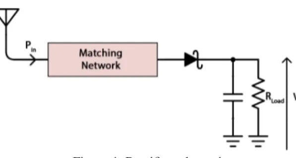
In order to provide the necessary power to our sensor node, we will consider an RF/DC converter (known also as rectifier) in the 2.45 GHz ISM band. We focus here on the conversion part and not on the antenna. Let us first of all establish an inventory of the evo-lution of the DC output voltage (V ) and of the con-version efficiency (η) in order to be able to define the axes of development on which it is necessary to work. We will start with the simplest RF/DC con-verter which is basic crest detector, based of a single Skyworks SMS7630 Schottky diode as presented on Fig.4.
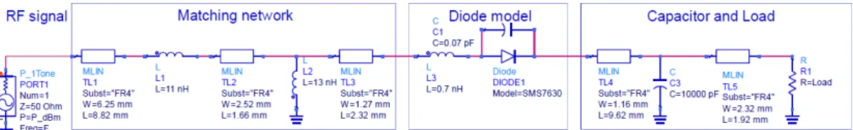
Matching network includes transmission lines and inductors and are determined thanks to simulations performed with Keysight Advanced Design System software in order to optimize impedance matching for maximum power transfer by minimizing signal reflex-ion between the antenna and the converter and also harmonics created by the Schottky diode due to its non linearities (Fig.5).
Figure 4: Rectifier schematic
We will therefore optimize the circuit parame-ters to maximize the DC output voltage for our load. Based on ON Semiconductor’s white papers, we can estimate the load resistance of the platform at about 1000 Ohm. Since the WiFi input power (Pin) will be
converted into DC power (PDC), we can then look at
the evolution of the efficiency (η) (Equ.(2)) and the DC output voltage (V ) for different arbitrary Pinon
table 1.
η =PDC Pin
(2)
Table 1: Output voltage and efficiency of the simple RD/DC converter Pin(dBm) η (%) V (mV) -30 5.7 8 -25 12 19 -20 20 45 -15 28 94 -10 34.6 186 0 42 648
The main problem with the RF/DC converter is the DC output voltage, which can be very low given the RF input power levels. Indeed, on current reception power levels for WiFi signal, the diode sees its effi-ciency drop because it is not sensitive enough. We can notice that we never obtain the needed 2.6 V voltage since the maximum obtained is 648 mV at 0 dBm. It is therefore necessary to work on a more elaborate con-version system to reach acceptable voltage levels. The state of the art on the subject mainly uses Cockcroft-Walton voltage doubler assemblies (Kee et al., 2018) which have the advantage of being able to be mounted in cascade to raise the voltage to our needs.
To limit the number of Cockcroft-Walton stages required, we can consider adding a boost like the BQ25504 from Texas Instruments or the LTC3105 from Analog Devices. We thus lower our target volt-age at the converter output down to about 300 mV in-stead of 2.6 V which relaxes our constraints. Indeed, the boost will thus provide an output voltage of 3.3 V with the 300 mV input voltage provided by the
recti-Figure 5: Keysight ADS schematic
Figure 6: One stage Cockcroft Walton voltage doubler
fier. It will then allow us to charge a capacitor up to our threshold voltage of 2.6 V.
Now that we have some answers about our voltage constraint, let’s look at the question of energy. Having seen in section 2.2 that it was possible to power our system given the amount of energy received at the an-tenna, is it still energetically viable after conversion?
4
Energy harvesting duty cycle
Let’s assume for this part that we have solved our volt-age concerns, so we can store energy using a capac-itor. How often can we expect to measure and send our data, i.e. store the 200 µJ needed to operate the sensor node?
4.1
Theoretical model
Firstly, we will start with a ideal converter with 100% efficiency (η = 1), what would then be the duty cy-cle (T ), i.e. how long would it take the converter to store the required 200 µJ in the capacitor in order to power the sensor node once the storage is reached? To answer this, we will use the Equ.(3).
T = E
PDC
= E
η.Pin
(3) So, for a Pinequal to -30 dBm, the duty cycle T will
be equal to 200 seconds. Table 2 displays the duty cycle (T ) for different Pin.
Thus, we won’t manage to get better than 200 sec-onds (3 minutes and 20 secsec-onds) between two transmissions with a permanent harvested power of -30 dBm. Because of the efficiency of our rectifier that is not ideal (table 1), we have to correct the estimated duty cycle (table 3) according to Equ.(3).
Table 2: Duty cycle with a perfect converter
Pin(dBm) T (s)
-30 200
-20 20
-10 2
0 0.2
Table 3: Duty cycle with a real converter
Pin(dBm) η (%) T (s)
-30 5.7 3509
-20 20 100
-10 34.6 6
0 42 0.48
We therefore notice a drastic drop in performance with a duty cycle from 200 seconds to 3509 seconds (around 58 minutes) at -30 dBm.
To get to the end of our approach, let’s suppose that to work we use the LTC3105 boost from Analog Devices that we mentioned in section 3. The datasheet of the component announces a minimum efficiency (η0) of 65% for an input voltage lower than 1 V which should be the case in the light of the study carried out in section 3. Let’s then consider the compute ef-ficiency (η.η0) to have an idea about the duty cycle in this worst case (table 4).
Table 4: Duty cycle by taking into account the boost effi-ciency Pin(dBm) η.η0(%) T (s) -30 3.7 5406 -20 13 154 -10 22.5 9 0 27.3 0.73
For a constant RF input power of -30 dBm, the result indicates a period of 5406 seconds (around 1 hours and 30 minutes) between two transmissions when using our RF converter associated to the DC boost.
So next step will be to consider a non-constant harvested power to have a closer approach for real conditions use case.
4.2
Application of the model
In order to determine the obtained amount of DC en-ergy harvested from real WiFi signal as displayed on Figure 2, we have first to model the efficiency η from the arbitrary RF input power Pin given by
ta-ble 1 using a polynomial function. Then, apply the obtained model to determine the converter efficiency η(t) associated to the available WiFi signal Pin(t)
measured (Fig.2). The available DC energy could be obtained after time integration of PDC(t) determined
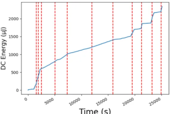
using Equ.(2) and is displayed Fig.7. Vertical lines indicate each time the capacitor store enough energy (200 µJ) to power the sensor node and the duration between two vertical lines are displayed table 5.
Figure 7: Amount of energy available to power the sensor node labelled
We can consider 11 transmissions on a 7-hour measurement of ambient WiFi signal. We can there-fore expect one data transmission every 38 minutes and 11 seconds on average.
5
Conclusion
We thus realized a measurement and simulation bench allowing to define, from Pin, the frequency at which
the system can send the data of its sensors. Even if the availability of electromagnetic energy is non con-stant, our work shows that powering such a system with ambient WiFi signals is energetically viable de-spite a low efficiency of 3.7% with a Pinof -30 dBm.
However, there is a optimization work to be done on the converter to overcome the low output voltage and reach the 300 mV threshold required, still for a Pinarround -30 dBm, to operate the voltage booster.
of the latter and to allow data to be sent at more regu-lar intervals in order to diversify the possible applica-tions. The use of a converter that extends over several
frequency ranges, such as for example combining the 2.45 GHz ISM band with GSM 1800 (Berg`es et al., 2015) can be a way of improving performance.
A study of the different sensors and microcon-trollers in the industry will also have to be carried out to compare and ensure that we have an optimal soft-ware layer with regard to power consumption.
REFERENCES
(2018). Les niveaux d’exposition WiFi. http://www.radiofrequences.gouv.fr/les-niveaux-d-exposition-a73.html.
Berg`es, R., Fadel, L., Oyhenart, L., Vigneras, V., and Taris, T. (2015). A dual band 915MHz/2.44GHz RF energy harvester. In 2015 European Microwave Conference (EuMC), pages 307–310. ISSN: null.
Bruno Damien, Tobias Raimar, L. M. (2019). Continu-ous Harvesters and ON Semiconductor’s LowPower rf technology close the gap in environmental and ac-celerometer Sensors for iot.
Ho, D.-K., Kharrat, I., Ngo, V.-D., Vuong, T.-P., Nguyen, Q.-C., and Le, M.-T. (2016). Dual-band rectenna for ambient RF energy harvesting at GSM 900 MHz and 1800 MHz. In 2016 IEEE International Conference on Sustainable Energy Technologies (ICSET), pages 306–310. ISSN: null.
Kee, C. P., Olule, L., and Gnanagurunathan, G. (2018). Microstrip Patch Antenna and Three-stage Cockcroft-Walton Rectenna for Wi-Fi Energy Harvesting. In 2018 IEEE International RF and Microwave Confer-ence (RFM), pages 242–245. ISSN: null.
Krakauskas, M., Sabaawi, A. M., and Tsimenidis, C. C. Suspended patch microstrip antenna with cut rect-angular slots for RF energy harvesting. In 2014 Loughborough Antennas and Propagation Conference (LAPC), pages 304–307. ISSN: null.
Kurvey, M. and Kunte, A. Design and optimization of stepped rectangular antenna for RF energy harvest-ing. In 2018 International Conference on Commu-nication information and Computing Technology (IC-CICT), pages 1–4. ISSN: null.
Parks, A. N., Sample, A. P., Zhao, Y., and Smith, J. R. (2013). A wireless sensing platform utilizing ambi-ent RF energy. In 2013 IEEE Topical Conference on Biomedical Wireless Technologies, Networks, and Sensing Systems, pages 154–156. ISSN: null. Shaker, M. F., Ghali, H. A., Elsheakh, D. M. N., and
El-sadek, H. A. E. Multiband coplanar monopole antenna for energy harvesting. In 2018 IEEE International Symposium on Radio-Frequency Integration Technol-ogy (RFIT), pages 1–3. ISSN: null.