HAL Id: hal-01941761
https://hal.inria.fr/hal-01941761
Submitted on 3 Dec 2018
HAL is a multi-disciplinary open access
archive for the deposit and dissemination of
sci-entific research documents, whether they are
pub-lished or not. The documents may come from
teaching and research institutions in France or
abroad, or from public or private research centers.
L’archive ouverte pluridisciplinaire HAL, est
destinée au dépôt et à la diffusion de documents
scientifiques de niveau recherche, publiés ou non,
émanant des établissements d’enseignement et de
recherche français ou étrangers, des laboratoires
publics ou privés.
A Diversity Scheme to Enhance the Reliability of
Wireless NoC in Multipath Channel Environment
Joel Ortiz Sosa, Olivier Sentieys, Christian Roland
To cite this version:
Joel Ortiz Sosa, Olivier Sentieys, Christian Roland. A Diversity Scheme to Enhance the Reliability
of Wireless NoC in Multipath Channel Environment. Twelfth IEEE/ACM International Symposium
on Networks-on-Chip (NOCS), Oct 2018, Torino, Italy. pp.1-8, �10.1109/NOCS.2018.8512165�.
�hal-01941761�
A Diversity Scheme to Enhance the Reliability of
Wireless NoC in Multipath Channel Environment
Joel Ortiz Sosa
Univ Rennes, Inria Lannion, France joel.ortiz-sosa@inria.fr
Olivier Sentieys
Univ Rennes, Inria Rennes, France olivier.sentieys@inria.fr
Christian Roland
UBS - Lab-STICC Lorient, France christian.roland@univ-ubs.frAbstract—Wireless Network-on-Chip (WiNoC) is one of the most promising solutions to overcome multi-hop latency and high power consumption of modern many/multi core System-on-Chip (SoC). However, the design of efficient wireless links faces challenges to overcome multi-path propagation present in real-istic WiNoC channels. In order to alleviate such channel effect, this paper presents a Time-Diversity Scheme (TDS) to enhance the reliability of on-chip wireless links using a semi-realistic channel model. First, we study the significant performance degradation of state-of-the-art wireless transceivers subject to different levels of multi-path propagation. Then we investigate the impact of using some channel correction techniques adopting standard performance metrics. Experimental results show that the proposed Time-Diversity Scheme significantly improves Bit Error Rate (BER) compared to other techniques. Moreover, our TDS allows for wireless communication links to be established in conditions where this would be impossible for standard transceiver architectures. Results on the proposed complete transceiver, designed using a 28-nm FDSOI technology, show a power consumption of 0.63mW at 1.0V and an area of 317 µm2. Full channel correction is performed in one single clock cycle.
Index Terms—Wireless Network-on-Chip, Channel Effects, Multi-Path Propagation, Communication Reliability, Digital Transceiver Architecture
I. INTRODUCTION
The emerging manycore architecture era comes up with critical issues in communication latency and power consump-tion. Network-on-Chip (NoC) was a very promising solution to solve these challenges. However, with the scaling of advanced CMOS technologies, the number of cores is continuously growing. As a consequence, the number of hops needed to communicate between cores creates a critical bottleneck in the communication backbone by increasing latency and power consumption due to large volume data transmission. To deal with the surge of high performance computing systems and to overcome this communication bottleneck, new interconnect technologies, such as 3D-NoC [1], Radio-Frequency Intercon-nects (RF-I) based on waveguides [2], Optical NoC [3] [4] and Wireless NoC [5], have emerged.
Although it is true that Wireless Network-on-Chip (WiNoC) is one of the most promising solutions for the communication infrastructure of chip multiprocessors (CMP) and multipro-cessor System-on-Chip (MPSoC), the reliability of on-chip wireless links is still an important and unsolved issue [6]. Indeed, most of the approaches from the literature estimate
performance using a very simplistic wireless channel model, which only considers path loss through free space and Additive White Gaussian Noise (AWGN). However, a realistic wireless channel model should consider some of the most important parasitic phenomena introduced by the physical structures of the chip (e.g. multi-path propagation), especially, when communication data rate is aiming at several tens of gigabits per second.
The main contributions of this paper are as follows:
• We demonstrate, by simulation, the significant
degrada-tion of wireless communicadegrada-tions facing multi-path prop-agation for current Wireless NoC architectures. Simula-tion is performed by adopting a proposed semi-realistic wireless channel models, based on the wireless intra-chip communication literature.
• We study traditional channel cancellation techniques to improve communication reliability and adapt them to the on-chip wireless communication context.
• We propose a digital transceiver architecture for each of
the adopted techniques and evaluate their performance, power consumption and area for a 28 nm FDSOI technol-ogy and show that this overhead is very small compared to the gain in communication reliability.
This paper is organized as follows. Section II highlights the main limitations in the state-of-the-art of current WiNoC architectures. In Section III, we present a semi-realistic chan-nel model, while in Section IV, we study the traditional wireless interfaces used in WiNoC and show their weaknesses. After introducing some techniques to improve communication reliability, we propose a new transceiver architecture in Sec-tion V. Finally, in SecSec-tion VI, we show some performance and synthesis results of the proposed architecture before to conclude in Section VII.
II. RELATEDWORK
Wireless Network-on-Chip (WiNoC) was proposed as a more feasible and promising solution that can scale with transistor technology and the ever-increasing number of cores in a NoC [7]. Most of the contributions in the literature attempt to demonstrate that the WiNoC paradigm can over-come the limitations of conventional multi-hop NoC archi-tectures for core-to-core [8], [9], and core-to-memory (e.g. cache coherency) [10], [11] communications. Many works
have also investigated different network topologies to take advantage of long distance links [12], [8]. WiNoC can thus allow for the reduction of energy consumption involved by transporting information packets through the network routers. The topology also impacts the total latency and throughput of the network [7].
Despite all these efforts to propose efficient WiNoC archi-tectures, the considered wireless channel model is very simple (i.e., using an additive white Gaussian noise) and therefore not representative of actual on-chip wireless channels. In particular, this basic model does not consider the frequency and time behavior of WiNoC for isotropic antennas, such as multi-path propagation and bandwidth limitation.
However, few prior works have introduced some interesting channel features that could be considered for WiNoC simu-lations. As an example, the authors of [13] give a general overview of the main WiNoC characteristics considering a two-ray channel model. Besides, their analysis concludes that on-chip wireless channel resembles to familiar terrestrial settings. An analytical channel model is proposed in [14]. This model introduces the concept of molecular absorption attenuation (MAA), which makes the wireless communication through the air unsustainable. In any case, both analyses con-sider multi-path propagation as an unavoidable phenomenon for intra-chip wireless communications. However, to the best of our knowledge, there is no work that considers during performance simulations the significant impact of multi-path propagation on the reliability of WiNoC communications. In contrast, the use of highly directive antennas based on carbon nanotube (CNT) is proposed in [15], which could avoid multi-path propagation. Nevertheless, CNT antennas are still facing many challenges to be fully integrated in current chip fab-rication process. Moreover, with such solution, broadcasting wireless signals will be hardly achievable without a dense antenna array. Other research studies around antennas designed for on-chip communications (e.g., [16], [17], [18]) also provide relevant information to build more realistic WiNoC channel models. However, the experimental setup only considers sim-ple scenarios such as point-to-point communications without effects of chip package and real multicore context as it should exist in WiNoC. Effects of wave propagation caused by using monopole or dipole antennas fabricated on silicon wafer as well as channel analysis for this simple type of communication are also proposed [19], [20], [21], [22].
III. CHANNELMODELING
In any wireless communication system, it is very important to estimate the channel characteristics. Depending on the channel, the design of the transceiver needs to ensure a certain degree of wireless link reliability, as well as to reach a trade-off in design complexity. WiNoC, as a specific scheme of intra-chip wireless communication, also requires a precise estima-tion of the channel. The channel must be modeled considering the parasitic phenomena introduced by the physical structure and electrical properties of all the components inside the chip, as well as the chip-package [14]. As a result, building an
accurate model of a WiNoC channel is important but it is also a complex task.
A wave propagated through a channel can suffer reflection, refraction and diffraction. Accordingly, waves can be propa-gated using different media at the same time. This approach was modeled and validated in [18], creating different ray paths through the silicon wafer. Besides, Zhang et al. [17] demon-strated that at least three types of waves on which the signal is propagated over intra-chip channel must be considered: space wave (air), surface wave (air-wafer interface), and guided wave (through silicon substrate). Likewise, their study concludes that the dominant path is not transmitted by space wave, but mainly by surface wave.
Furthermore, the resistivity of the silicon substrate is a very important parameter for intra-chip wireless communi-cation. Propagating waves through a low-resistivity ( ρ = 10 − 20 Ω · cm) or a high-resistivity ( ρ ≥ 5 kΩ · cm) mate-rial, can significantly affect signal attenuation. Moreover, as demonstrated in [19], the influence of multi-path fading effects is more important for low-resistivity silicon substrate and for shorter distances.
Also, a delay spread was measured for different antennas (zigzag, meander, and linear) in [17]. It was observed that the delay spread generally increases with the transmitting and receiving antennas (T-R) separation, although delay spread for a specific channel impulse response (CIR) depends on the surrounding of the T-R pair. For instance, a delay spread for a distance of 10 mm, using zigzag monopole-pair with some interference structures, is120 ps.
In this paper, to estimate and analyze the impact of a semi-realistic channel, the provided simulations are based on the previously discussed models defined for intra-chip wave propagation. We consider that a channel impulse response should include at least two propagation paths for realistic WiNoC simulations together with Additive White Gaussian Noise (AWGN). Obviously, the number of paths is dependent on the symbol duration. For instance, considering a data rate up to 32 Gbit/s for WiNoCs, the symbol duration will be as small as 32.25ps, which is four time smaller than the delay spread for a distance of10 mm. This indicates that the number of significant paths could be up to three, each one separated by a symbol duration.
On the other hand, due to the low complexity of its implementation, the classical modulation scheme considered for WiNoCs is On-Off Keying (OOK) with a maximum data rate of 16 Gbit/s. However, other modulation schemes (BPSK, QPSK, 16-QAM, etc.) can provide better spectral efficiency and higher resilience to multi-path propagation, although con-suming more power and area than OOK.
In order to test the reliability of current WiNoCs facing multi-path propagation, Fig. 2 represents the Bit-Error Rate (BER) of an OOK transceiver as a function of the Signal-to-Noise Ratio (SNR) per bit in various multi-path conditions. Our simulations consider a two-ray model, and a time-invariant frequency-selective channel impulse response (CIR) composed of only two paths (the direct and the reflected paths), separated
Figure 1: Channel impulse response with α= 60%
by a symbol duration, as shown in Fig. 1. Also, the gain of the reflected path, defined as a percentage of the direct one, varies from α = 0% to α = 60%. As observed in Fig. 2, the communication starts to degrade rapidly as soon as the reflected-path gain increases, even with small values of α. The degradation becomes significant even if the amplitude of second path is only 30% of the main path. For this reason, multi-path cancellation techniques and their respective architectures are required to increase reliability of WiNoC communications.
Figure 2: Scaling of BER performance according to the SNR per bit (Eb/N0) for different reflected-path gains in the OOK
scheme.
IV. OPTIMIZING THEWINOC COMMUNICATIONSCHEME
In this section, we first detail the basic communication scheme for WiNoCs and then introduce our modifications to increase communication reliability. Moreover, to overcome the CIR presented in the above section, we introduce some techniques used in traditional wireless communication systems to decrease channel effects.
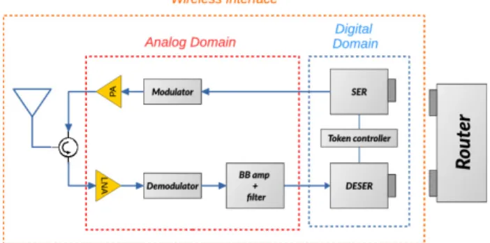
A. Traditional Wireless Interface
A traditional Wireless Interface (WI) connects a conven-tional router/switch with the wireless medium. The WI can be divided into three main parts: antenna, analog and digi-tal blocks, as shown in Fig. 3. The digidigi-tal domain mainly incorporates the channel access token controller and a Se-rializer/Deserializer. The analog domain includes an On-Off
Keying (OOK) transceiver module, which has a very low complexity compared to other modulation schemes. There exist several architectures proposed in literature for the OOK transceiver, considering coherent or non-coherent detection [23], [24], [25]. Moreover, power consumption reduction mechanisms can be applied [5], which would allow to optimize the power according to the distance.
Figure 3: A conventional Wireless Interface of a WiNoC. The communication between the router/switch and the WI begins with the source core setting the corresponding message into the Network Interface (NI) module. The NI packetizes the message by breaking it into several flits (such as header, payload, tailer). The router/switch is then used to forward the data flits into the wired interconnection network or towards the WI, whether the token flow controller (TFC) authorizes the use of the wireless medium. The data flits will be converted into a serial data stream using the serializer (SER) block. Then the OOK modulator adapts the baseband frequency signal into a high frequency one (carrier frequency). The signal obtained is transmitted to the power amplifier (PA), which delivers the required transmitting power. Finally, this amplified signal is spread through the wireless medium using a dedicated or shared antenna. In case of a shared antenna, a nonmagnetic nonreciprocal passive CMOS circulator [26] allows for full-duplex (frequency-division duplexing) or half-duplex communication.
At the receiver side, once the signal reaches the antenna, it is intensified by a low noise amplifier (LNA). Then, a demodulator shifts the high frequency signal into a baseband one. The next step is to amplify and filter the serial baseband signal, which is converted into a parallel data stream of flits using the deserializer (DESER) block. Finally, considering that the destination core is connected directly to the router/switch, the received flits will be conducted towards the NI to retrieve the message forwarded by the source core.
B. Improving Communication Reliability
To the best of our knowledge, current transceiver solutions from WiNoC literature do not consider some channel effect cancellation mechanisms, even during performance simula-tions. In this paper, we therefore study, simulate and synthesize traditional channel cancellation techniques adapted to on-chip wireless communications. One reasonable hypothesis of
this work is that the WiNoC channel is time invariant. This characteristic prevents the use of complex adaptive filtering al-gorithms for WiNoC communications. Finally, the theoretical and mathematical approaches of each considered technique is obtained from [27].
1) Equalization Techniques: are widely studied in con-ventional wireless communication to compensate for Inter Symbol Interference (ISI) created by multi-path propagation. Equalization can be linear (e.g., Zero Forcing, Minimum Mean Square Error) and non-linear (e.g. Decision Feedback Equalizer). The effectiveness of multi-path cancellation varies widely in practice, according to the type of equalizer applied. Furthermore, hardware cost and computation complexity are important issues when equalization is adopted.
In this section we analyze the impact of Zero-Forcing (ZF) linear equalization, which is less complex than other equaliza-tion techniques. ZF restores the received signal applying the inverse of the channel frequency response computed off-line or on-line. Normally, a linear transverse filter is used when this technique is adopted. The coefficients bi of the filter can
be calculated in the time domain from the CIR, by resolving the following matrix system
h0 0 0 0 0 h1 h0 0 · · · 0 h2 h1 · · · · · · · h0 0 hk−1 · · · h2 h1 h0 b0 b1 b2 · · · bk−1 = 0 · · · 1 · · · 0 (1)
where hi are the multi-path components of the CIR and k the
total number of ZF filter coefficients is an odd integer value. As an example following Fig. 1, h0 = 1, h1 = α and hi = 0,
∀ i= 2 . . . k − 1.
The impact of using the ZF technique is simulated with different number of coefficients (i.e., taps) k using the CIR with α= 60% as defined in Section III. As shown in Fig. 4, the multi-path cancellation efficiency improves with the number of coefficients. However, a large number of taps occupies sig-nificant area and consumes a relatively high amount of power, especially when computed at high frequency. Furthermore, even with a large number of coefficients, the simulated BER will never match the theoretical OOK BER. This phenomenon occurs because the zero-forcing equalizer amplifies the noise power during the signal filtering process.
2) Direct Sequence Spread-Spectrum (DSSS): is a trans-mission technique used in wireless network communications where a data signal at the sending node is combined with a code sequence (e.g. Gold sequence, M-sequence, Hadamard codes) running at high frequency, the chip rate. DSSS com-bines users’ data based on a spreading factor (SF) defined as the chip rate divided by the symbol (data) rate. The main advantages of DSSS are a resistance to jamming and inter-ference, less background noise, and a certain degree of multi-path resilience depending on the code sequence characteristics. Furthermore, DSSS allows for multiple users to access the same channel simultaneously in synchronous or asynchronous mode. In the WiNoC literature, this technique was adopted by
Figure 4: Demodulation performance BER according to the SNR per bit (Eb/N0) using Zero-Forcing equalizer with
dif-ferent number of filter taps.
[28], demonstrating promising results over conventional NoCs. However, simulations and performance estimations provided in [28] were only considering an ideal wireless channel.
3) Time-Diversity Scheme (TDS): implies that the same data is transmitted repeatedly at different time schedule. Thus, considering a channel with multi-path propagation, there are multiple copies of the same signal transmitted according to the number of multi-path components. Therefore, as depicted in Fig. 5, DSSS also takes advantage of this characteristic assuming L correlators between the input data signal y(t) and code sequences delayed by i = 0 . . . L − 1 chip periods. The correlator outputs are combined using a diversity combining rule with their respective weighting coefficients (Gi). On the
other hand, since this technique collects the energy from the received signal components to provide diversity, it is often called the RAKE receiver.
Figure 5: Diversity demodulator for spread-spectrum signals over multi-path channels.
V. ARCHITECTURE OF THEWIRELESSINTERFACE
This section presents the WiNoC and wireless transceiver architectures considered in this work.
A. WiNoC Architecture
1) Topology: The adopted topology is based on a wired 2-D mesh conventional NoC architecture, divided into N clusters including a wired sub-network. Each cluster has one Wireless Interface (WI) connected to a dedicated router/switch, responsible for providing wireless access to the cores placed in the same cluster. Fig. 6 illustrates a 20mm × 20mm chip example composed of8 × 8 cores. The WiNoC architecture is divided into N = 4 clusters of 16 cores with a WI located at the center of each cluster.
2) Wireless Multiple Access: Due to the availability of multiple channels, the synchronous DSSS technique is adopted for channelization to achieve simultaneous multiple commu-nications among the WIs. Each cluster i uses a dedicated code sequence Ci for data transmission and knows the code
sequence of the other clusters for data demodulation at the receiver side. Besides, we consider that signal synchronization is performed only once in the WI to open the different simultaneous channels.
Figure 6: Wireless interface distribution among a clustered WiNoC hybrid topology with N = 4 clusters.
B. Wireless Interface Architecture
The adopted WI architecture is similar to the one ex-plained in Section IV-A. However, the digital domain part is modified to comply with the proposed techniques. Fig. 7 depicts the global architecture of the digital transceiver, which is divided into three parts classified by clock frequencies: low 1 , medium 2 and high 3 . Furthermore, zero-forcing equalization and time diversity scheme are implemented using DSSS as a baseline architecture. Therefore, in our simula-tion and synthesis results, we tested three main architecture configurations detailed in this section and shown in Fig. 7: DSSS, TDS with DSSS, and ZF with DSSS. Additionally, DSSS needs an analog-to-digital converter (ADC) block to distinguish each code-channel. Consequently, to avoid exces-sive area cost and power consumption, we propose to adopt a 10 Giga-samples-per-second Time-Interleaved Successive Approximation Register (SAR) ADC [29] instead of a flash ADC. This ADC provides eight 4-bit words in parallel at 1.25 GHz corresponding to eight consecutive samples.
Despite the use of serializer (SER) and de-serializer (DESER) blocks is mandatory in any wireless communication,
previous WiNoC literature rarely details information about these blocks. Therefore, we propose to adopt a SER/DESER binary MUX tree topology with half-rate architecture [30], [31], which uses a 625 MHz half-rate clock source to generate 1.25 Gb/s data rate. In addition, this architecture is a good compromise between higher data rates and risks of duty-cycle distortion and clock skew.
Figure 7: Enhanced digital-domain transceiver architecture with three decoder configurations.
1) DSSS Architecture: is divided into two main functional blocks: encoder and decoder. Furthermore, the code sequence adopted in this architecture is a Hadamard binary code on 8 bits (SF= 8). As each cluster has a dedicated code sequence, the design of the encoder block is very simple. The encoder is composed of registers whose outputs are arranged according to the Hadamard code sequence assigned to the considered cluster.
The decoder, depicted in Fig. 8, is a dedicated block used to retrieve the information forwarded by other clusters. As a
Figure 8: DSSS decoder architecture.
consequence, the decoder is composed of one correlator for each block with which it communicates, using the respective code sequence assigned to the considered cluster. As an example, for the architecture of Fig. 6 with four clusters, three correlators will be used in each cluster. Each correlator receives eight 4-bit words Dj in parallel from the ADC, with
Dj ∈ {0, 1, ..., 15} and j = {0, 1, ..., 7}. These Dj input values
are directly compared with the jth bit of code Ci, jrelated to the
ith cluster. Consequently, the value of Dj is turned to negative
if the jth bit is 1, and remains positive otherwise. Then, the correlator performs addition or subtraction operations to
calculate
Corr= ±D0± D1± D2± D3± D4± D5± D6 ± D7. (2)
The final step is to make a decision based on the resulting value of Corr, using a threshold detector. The optimal thresh-old value for DSSS with OOK modulation using Hadamard codes is 0. In our case, the decoder output is 1 when corr <0 and 0 when corr > 0. This decision operation is simplified by connecting the sign bit (the MSB as we consider two’s complement representation) of the resulting value of Corr directly to the decoder block output.
2) TDS with DSSS architecture: uses the same encoder block architecture, as explained in the previous section. How-ever, the decoder, depicted in Fig. 9, increases the number of correlators used by cluster code sequence according to the number of significant multi-path components (MPC) estimated from the CIR. As the architecture is designed using the CIR
Figure 9: Decoder architecture of the time diversity scheme. studied in Section III with α= 60%, two correlators are used by code sequence to retrieve the forwarded information from one cluster. The first one compares the input values Dj with
the jth bit of code Ci, jrelated to the ith cluster and the second
one compares Dj with a time-shifted version of Ci, j. Then the
correlation results are combined using a diversity combining rule, called Maximum Ratio Combining (MRC). The MRC uses weighting coefficients obtained from the CIR to combine the correlator outputs. Finally, the sign bit (MSB) of the resulting combination value obtained from MRC computation is connected directly to the decoder block output.
To illustrate the correlator and MRC operations, Fig. 10 displays one Hadamard code with its one time-shifted version. These codes are processed by the correlators and the MRC
Figure 10: Time-diversity scheme optimization.
combiner as follows:
Corr0 = −D0− D1− D2− D3+ D4+ D5+ D6 + D7
Corr1 = D0− D1− D2− D3− D4+ D5+ D6 + D7
M RC = G0× Corr0+ G1× Corr1 (3)
3) TDS Decoder Optimization: is performed by grouping the similar bits of the code sequences and their time-shifted version, as shown in Fig. 10. Generally, Hadamard codes contain similarities with their time-shifted version. Therefore, this characteristic is exploited to decrease the number of operations in a correlator by rewriting Eq. 3 as
Corr0 = −D1− D2− D3+ D5+ D6 + D7
Corr1 = −D0+ D4
M RC = G0× (Corr0+ Corr1)+ G1× (Corr0− Corr1)
4) Zero Forcing with DSSS Architecture: uses the same encoder block as the simple DSSS architecture. The decoder block, as illustrated in Fig. 11, is composed of three main sub-blocks: a circular buffer (CB), a ZF filter to mitigate multi-path propagation and a DSSS correlator with a code sequence. The coefficient values of the ZF filter are calculated from Eq. 1 using the CIR of Section III with α= 60%.
Figure 11: ZF equalizer with DSSS decoder architecture. VI. RESULTS
To evaluate the performance metrics of the different tech-niques studied in Section V, an end-to-end wireless com-munication system has been implemented for simulation and hardware synthesis. The effectiveness of each technique is evaluated adopting the multi-path channel characteristics de-scribed in Section III. The system under study is first simulated in MATLAB to estimate the BER performance. Then, the different architectures are modeled in C/C++ for High-Level Synthesis (HLS). Each architecture is synthesized to RTL using Catapult HLS and to the gate level by Synopsys Design Compiler. A 28-nm FDSOI technology library is used during hardware synthesis as a target with a supply voltage of 1 Volt. Finally, power consumption is estimated with Synopsys PrimeTime tool after activity extraction from a back-annotated gate-level simulation using3.2 × 105 random input data. A. Bit Error Rate Evaluation
The end-to-end system modeled in MATLAB considers a half-duplex communication and consists of four wireless interfaces to open three code-channels simultaneously. Each code-channel uses a dedicated orthogonal Hadamard code of 8 bits. The channel model employed in simulation was two-ray time-invariant frequency-selective channel with AWGN.
The modulation scheme simulated was coherent OOK. The simulated model considers the quantization noise (QN) added in the demodulation process by a 4-bit ADC at the receiver side [32]. The average BER, which considers three parallel code-channels, is estimated by Monte-Carlo simulation with a confidence interval of 95%.
Simulation results are reported in Fig. 12 for four different architectures: DSSS, DSSS with ZF using 3 taps and 11 taps, and DSSS with TDS. The considered techniques are compared with the single channel simulated BER of OOK with multi-path using α = 60%, and without multi-path channel (OOK Theory in Fig. 12). The results indicate that the average BER of the DSSS technique, without channel compensation, stays high even with an SNR per bit of 27 dB. This poor BER performance is due to the impact of the CIR on the code orthogonality, and consequently on the mis-detection rate. Nevertheless, associating DSSS with TDS or ZF improves performance compared with the technique without compensation. Indeed, part of the channel degradation was corrected, thus decreasing the mis-detection rate. Furthermore, comparing ZF filter using 3 taps with the other architectures on an average BER of e.g.10−6, shows that TDS and ZF with 11 taps improve the SNR by 5 and 8 dB, respectively. How-ever, despite ZF with 11 taps provides best performance, its complexity is much higher compared to the other architectures.
Figure 12: Demodulation performance BER scaling according to SNR for the considered techniques with α= 60%. B. Synthesis Results and Discussion
The different blocks of the digital transceiver as depicted in Fig. 7 have been synthesized from C/C++ using HLS and logic synthesis. Digital interfaces with the router are designed considering a 32-bit bus width, which is serialized at 1.25 Gbit/s by the 32-bit SER/DESER blocks described in Section V-B. The DSSS Encoder block encodes each data bit in a parallel stream of 8 bits, before being serialized at 10 Gbit/s by the 8-bit SER block.
Four different architectures (DSSS, DSSS with 3-tap ZF, DSSS with 11-tap ZF, and DSSS with TDS) are synthesized
separately. Each architecture configuration is capable to re-trieve data from N −1 clusters among N . Synthesis results of each architecture with N= 4 and other blocks of the wireless interface are summarized in Table I. Codec in the table means both the encoder and the considered decoder architecture configuration. The Optimized TDS Codec corresponds to the scheme proposed in Section V-B3.
The total power consumption of each block reports both the static and dynamic power consumed. However, static power represents less than 1% of the total power, mainly thanks to the 28-nm FDSOI low leakage technology. To estimate an accurate dynamic power, a Pseudo Random Bit Sequence of 4 × 104 bits is injected into the encoder block, which generates a total of 3.2 × 105 bits for the decoder block.
The ADC is a key block in OOK transceivers based on DSSS and filter compensation (e.g. zero-forcing) since it consumes the bulk of area and power of the WI. Nevertheless, as performance simulations in literature only consider an ideal wireless channel, no ADC is used for digital channel compen-sation. The parallel architecture of time-interleaved SAR ADC, mentioned in Section V-B, allows to decrease the frequency for digital filters and therefore to improve power consumption. Based on [29], Table I also provides area and power for the ADC block. For reference, figures extrapolated from [33] of an OOK transceiver are also reported. However, Section III already showed the poor performance of this transceiver in case of multi-path CIR.
Table I: Synthesis results (area and power consumption) of the different Wireless Interface architectures using 28-nm FDSOI.
WI Block Area (µm2) Power (mW )
DSSS Codec 313.18 0.43
TDS Codec 401.63 0.82
Optimized TDS Codec 317.42 0.63 3-tap ZF with DSSS Codec 490.41 0.98 11-tap ZF with DSSS Codec 1967.37 4.04 8-bit Serializer (10 Gbps) 21.8 0.1741 32-bit Serializer (1.25 Gbps) 49 0.04391 32-bit Deserializer (1.25 Gbps) 50 0.044
4-bit ADC [29] 9000 16
OOK Transceiver [33] not specified 20.8
The DSSS codec shows lower area and power consumption overhead than the other techniques. However, as shown in Fig. 12, its average BER is lower than for the other techniques with channel effect compensation. On the other hand, the ZF with 11 taps shows the best performance in terms of average BER, at the cost of highest power and area overhead. Finally, the average BER performance of the Time Diversity Scheme (TDS) based on the RAKE receiver is situated between ZF with 11 taps and 3 taps. In addition, the area and power consumption overhead of the optimized TDS codec is better than any k-tap ZF codec.
Furthermore, as shown in Fig. 2, decreasing α, the am-plitude of the second path of the CIR, improves BER per-formance. Therefore, any technique applied with α less than 60% will enhance BER too. However, the area and power consumption of each architecture will be approximately the
same (overhead may depend upon the coefficient values), but the TDS performance will become closer to the 11-tap ZF. Under these conditions, the TDS technique offers the best trade-off between BER performance and area/power over the other techniques.
VII. CONCLUSIONS
Emerging WiNoC communication technology is considered as a very viable solution for facing scalability and energy issues in multicore architectures. However, communication re-liability through a realistic wireless channel cannot be ensured by adopting conventional transceiver architectures. Therefore, in this paper, we show the impact of a semi-realistic multi-path wireless channel over conventional WiNoC modulation scheme. Our study demonstrates the significant unreliability of an OOK transceiver, even for a channel with low dispersion. To overcome this issue, we propose to combine the DSSS coding scheme with channel compensation blocks. Among the solu-tions studied, the TDS receiver represents the best trade-off between bit-error rate performance and area/power overhead, when compared with different Zero-Forcing equalizers. The area (and power) overhead of the TDS block for a four-cluster receiver is only317µm2 (and0.63mW ), which represents less
than 1% (2%) of the wireless interface. Therefore, the gain in performance of our proposed scheme is significant at the cost of a very low area/power overhead. The TDS, unlike an error-correcting code, offers more throughput as the number of users sharing the wireless channel increases. We believe that the introduction of the proposed solution opens interesting scenarios to combat channel effects in WiNoC.
REFERENCES
[1] S. Das et al., “Energy-efficient and reliable 3D Network-on-Chip (NoC): Architectures and optimization algorithms,” in Proc. IEEE/ACM Inter. Conf. on Computer-Aided Design (ICCAD), 2016, pp. 1–6.
[2] M. ValadBeigi, F. Safaei, and B. Pourshirazi, “An Energy-Efficient Reconfigurable NoC Architecture with RF-Interconnects,” in Proc. Eu-romicro Conf. on Digital System Design, 2013, pp. 489–496. [3] L. Guo, W. Hou, and P. Guo, “Designs of 3D mesh and torus optical
Network-on-Chips: Topology, optical router and routing module,” China Communications, vol. 14, no. 5, pp. 17–29, 2017.
[4] Z. Chen, H. Gu et al., “A Power Efficient and Compact Optical Inter-connect for Network-on-Chip,” IEEE Computer Archi. Letters, vol. 13, no. 1, pp. 5–8, 2014.
[5] A. Mineo, M. Palesi et al., “Runtime Tunable Transmitting Power Technique in mm-Wave WiNoC Architectures,” IEEE Trans. on VLSI Systems, vol. 24, no. 4, pp. 1535–1545, 2016.
[6] A. Karkar, T. Mak et al., “A survey of emerging interconnects for on-chip efficient multicast and broadcast in many-cores,” IEEE Circuits and Systems Magazine, vol. 16, no. 1, pp. 58–72, 2016.
[7] A. Ganguly, K. Chang et al., “Performance evaluation of wireless net-works on chip architectures,” in Proc. Inter. Symp. on Quality Electronic Design, 2009, pp. 350–355.
[8] P. P. Pande, A. Ganguly et al., “Hybrid wireless network on chip: A new paradigm in multi-core design,” in Proc. Inter. Workshop on NoC Archi., 2009, pp. 71–76.
[9] D. DiTomaso, A. Kodi et al., “A-WiNoC: Adaptive Wireless Network-on-Chip Architecture for Chip Multiprocessors,” IEEE Trans. on Parallel and Distributed Systems, vol. 26, no. 12, pp. 3289–3302, 2015. [10] A. Kayi et al., “Adaptive Cache Coherence Mechanisms with
Producer-Consumer Sharing Optimization for Chip Multiprocessors,” IEEE Trans. on Computers, vol. 64, no. 2, pp. 316–328, 2015.
[11] A. Asaduzzaman, K. K. Chidella, and D. Vardha, “An Energy-Efficient Directory Based Multicore Architecture with Wireless Routers to Min-imize the Communication Latency,” IEEE Trans. on Parallel and Dis-tributed Systems, vol. 28, no. 2, pp. 374–385, 2017.
[12] R. G. Kim, W. Choi et al., “Wireless NoC for VFI-Enabled Multicore Chip Design: Performance Evaluation and Design Trade-Offs,” IEEE Trans. on Computers, vol. 65, no. 4, pp. 1323–1336, 2016.
[13] D. W. Matolak, S. Kaya et al., “Channel modeling for wireless networks-on-chips,” IEEE Comm. Magazine, vol. 51, no. 6, pp. 180–186, 2013. [14] M. O. Agyeman, Q. T. Vien et al., “An Analytical Channel Model for
Emerging Wireless Networks-on-Chip,” in Proc. IEEE Inter. Conf. on Comp. Science and Engineering (CSE), 2016, pp. 9–15.
[15] A. Ganguly, P. Pande et al., “A Unified Error Control Coding Scheme to Enhance the Reliability of a Hybrid Wireless Network-on-Chip,” in Proc. IEEE Inter. Symp. on Defect and Fault Tolerance in VLSI and Nanotech. Systems, 2011, pp. 277–285.
[16] J. J. Lin, H. T. Wu, and Y. Su, “Communication Using Antennas Fabricated in Silicon Integrated Circuits,” IEEE Journal of Solid-State Circuits, vol. 42, no. 8, pp. 1678–1687, 2007.
[17] Y. P. Zhang, Z. M. Chen et al., “Propagation Mechanisms of Radio Waves Over Intra-Chip Channels With Integrated Antennas: Frequency-Domain Measurements and Time-Frequency-Domain Analysis,” IEEE Trans. on Antennas and Propagation, vol. 55, no. 10, pp. 2900–2906, 2007. [18] K. Kim, W. Bomstad, and K. O. Kenneth, “A plane wave model
approach to understanding propagation in an intra-chip communication system,” in Proc. IEEE Antennas and Propag. Society Inter. Symp. Digest., vol. 2, 2001, pp. 166–169 vol.2.
[19] Y. P. Zhang, M. Sun, and W. Fan, “Performance of integrated antennas on silicon substrates of high and low resistivities up to 110 GHz for wireless interconnects,” Microwave and Optical Tech. Letters, vol. 48, no. 2, pp. 302–305, 2006.
[20] A. Hajimiri, “mm-Wave Silicon ICs: Challenges and Opportunities,” in Proc. IEEE Custom Integrated Circuits Conf., 2007, pp. 741–747. [21] A. Babakhani, X. Guan et al., “A 77-GHz Phased-Array Transceiver
With On-Chip Antennas in Silicon: Receiver and Antennas,” IEEE Journal of Solid-State Circuits, vol. 41, no. 12, pp. 2795–2806, 2006. [22] K. Kim, H. Yoon et al., “On-chip wireless interconnection with
inte-grated antennas,” in Proc. Inter. Electron Devices Meeting (IEDM), 2000, pp. 485–488.
[23] X. Yu et al., “A 1.2-pJ/bit 16-Gb/s 60-GHz OOK Transmitter in 65-nm CMOS for Wireless Network-On-Chip,” IEEE Trans. on Microwave Theory and Techniques, vol. 62, no. 10, pp. 2357–2369, 2014. [24] X. Yu, H. Rashtian et al., “An 18.7-Gb/s 60-GHz OOK Demodulator in
65-nm CMOS for Wireless Network-on-Chip,” IEEE Trans. on Circuits and Systems I: Regular Papers, vol. 62, no. 3, pp. 799–806, 2015. [25] X. Yu, et al., “Architecture and design of multichannel millimeter-wave
wireless noc,” IEEE Design Test, vol. 31, no. 6, pp. 19–28, 2014. [26] N. Reiskarimian et al., “A CMOS Passive LPTV Nonmagnetic
Circu-lator and Its Application in a Full-Duplex Receiver,” IEEE Journal of Solid-State Circuits, vol. 52, no. 5, pp. 1358–1372, 2017.
[27] Proakis, Digital Communications 5th Edition. McGraw Hill, 2007. [28] A. Vidapalapati, V. Vijayakumaran et al., “NoC architectures with
adaptive Code Division Multiple Access based wireless links,” in Proc. IEEE Inter. Symp. on Circuits and Systems, 2012, pp. 636–639. [29] S. L. Tual et al., “22.3 A 20GHz-BW 6b 10GS/s 32mW time-interleaved
SAR ADC with Master T&H in 28nm UTBB FDSOI technology,” in Proc. IEEE Inter. Solid-State Circuits Conf. (ISSCC), 2014, pp. 382–383. [30] R. Clarke, M. R. LeRoy et al., “140 Gb/s Serializer Using Clock Doublers in 90 nm SiGe Technology,” IEEE Journal of Solid-State Circuits, vol. 50, no. 11, pp. 2703–2713, 2015.
[31] S. A. Mohammed, S. A. Ibrahim, and S. E. D. Habib, “6-Gb/s serial link transceiver for NoCs,” in Proc. IEEE Inter. Conf. on Electronics, Circuits, and Systems, 2015, pp. 425–428.
[32] N. F. Kiyani, P. Harpe, and G. Dolmans, “Performance analysis of ook modulated signals in the presence of adc quantization noise,” in IEEE Vehicular Technology Conference, 2012, pp. 1–5.
[33] K. Duraisamy, Y. Xue et al., “Multicast-aware high-performance wire-less network-on-chip architectures,” IEEE Trans. onVLSI Systems, vol. 25, no. 3, pp. 1126–1139, 2017.